

Growth and Characterization of Centimeter-Scale Pentacene Crystals for Optoelectronic Devices
 , , ,
, , ,
Abstract
1. Introduction
2. Experimental Section
2.1. Materials
2.2. Differential Scanning Calorimetry (DSC) and Thermogravimetry (TG)
2.3. Crystal Growth and Analysis
2.4. X-ray Diffraction
2.5. Absorption and Luminescence Spectra
2.6. Elemental Analysis
2.7. Electrical Properties
3. Results and Discussion
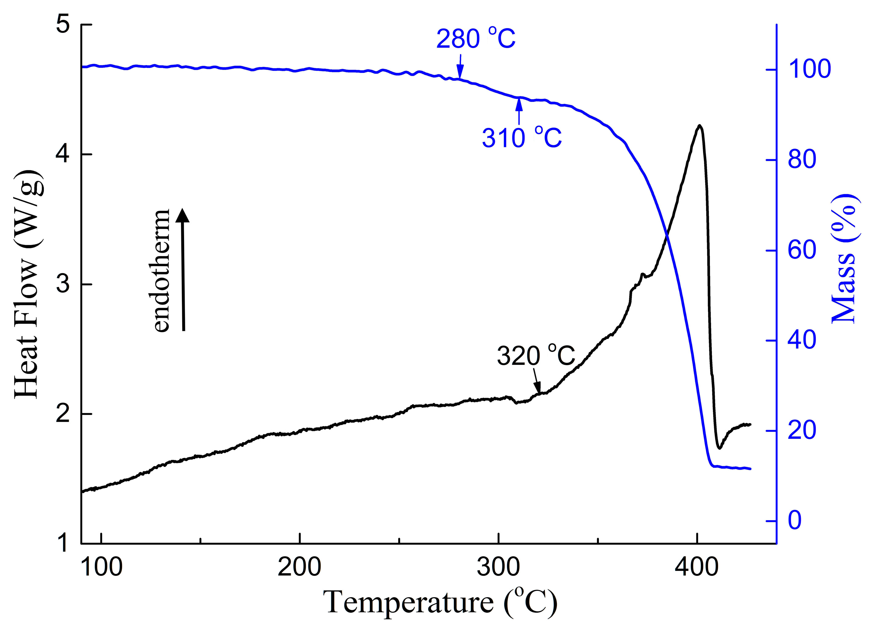
3.1. DSC and TG
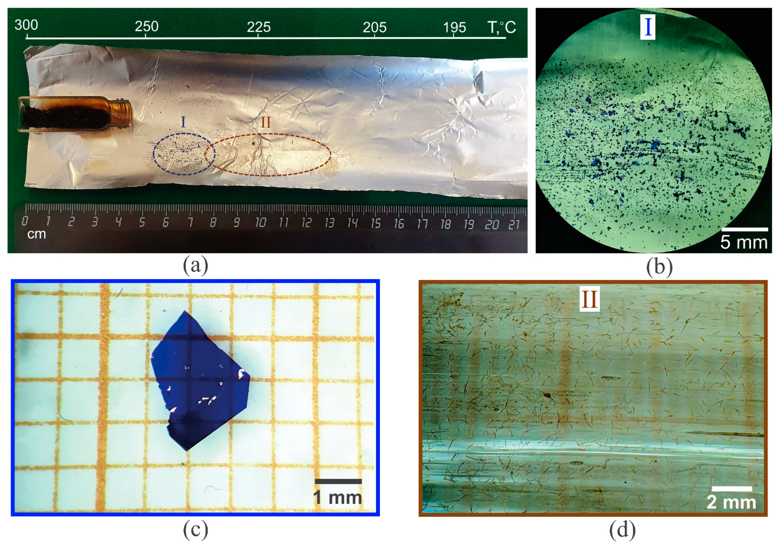
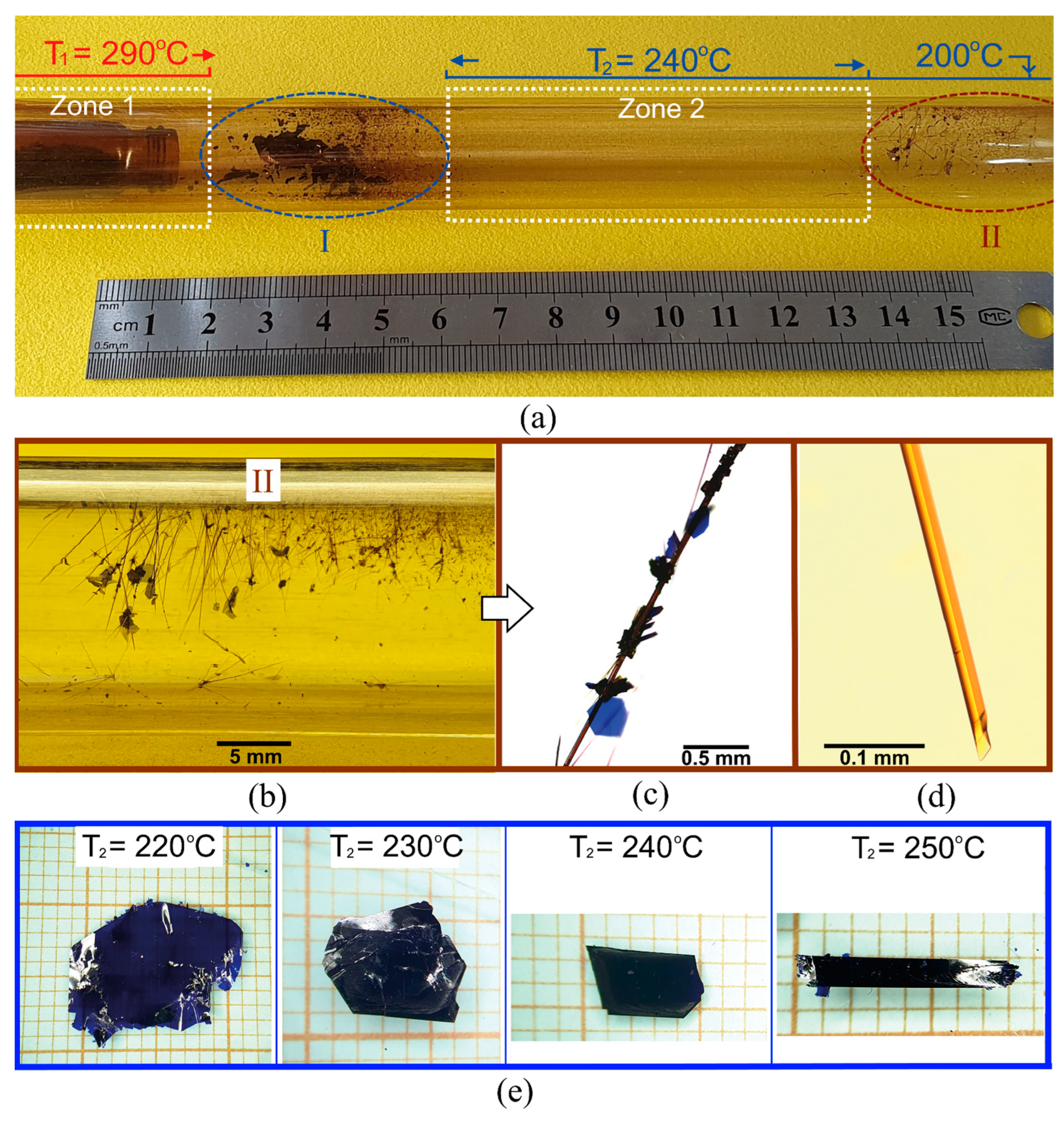
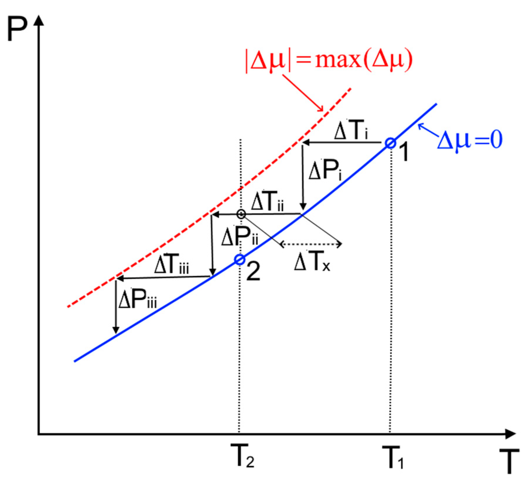
3.2. Crystal Growth
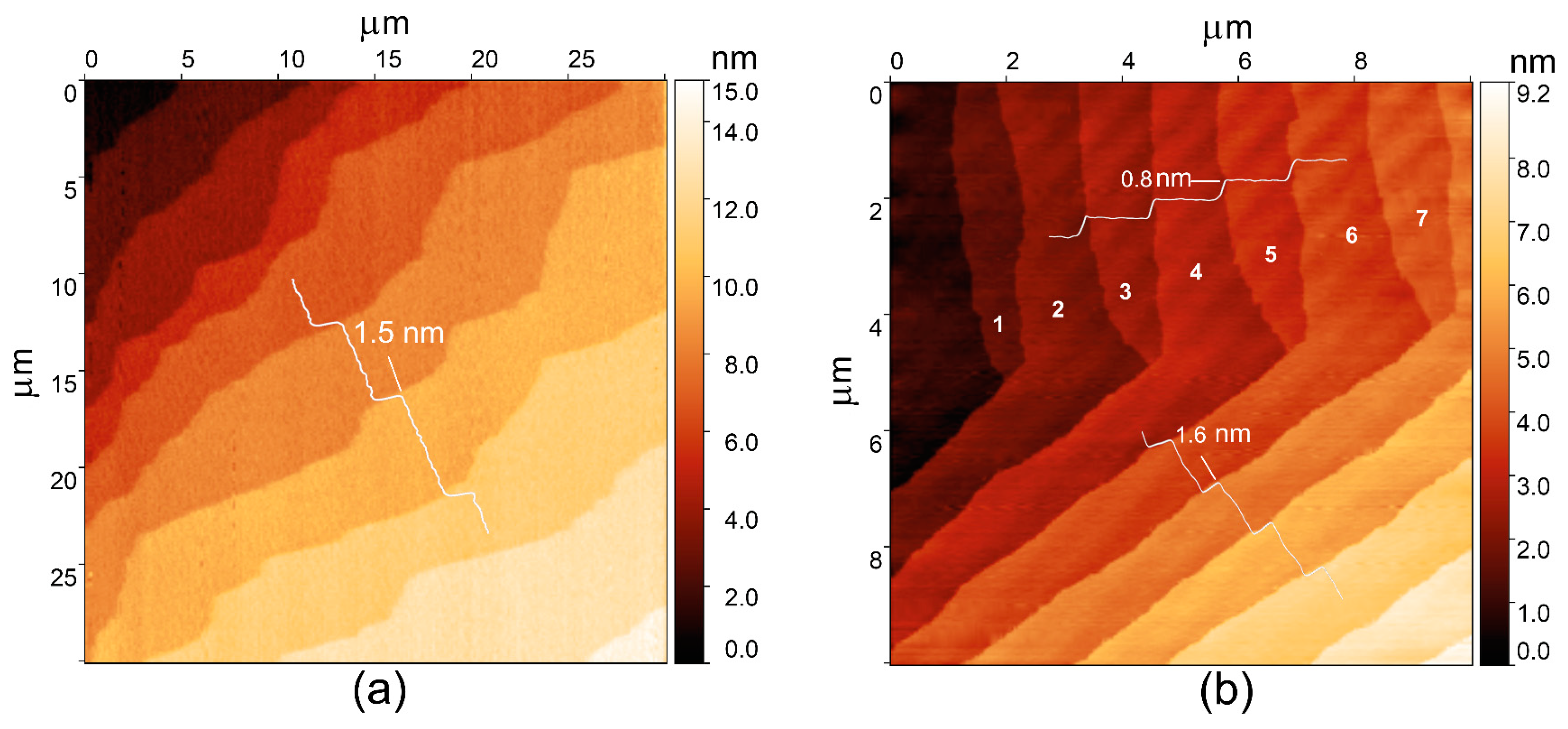
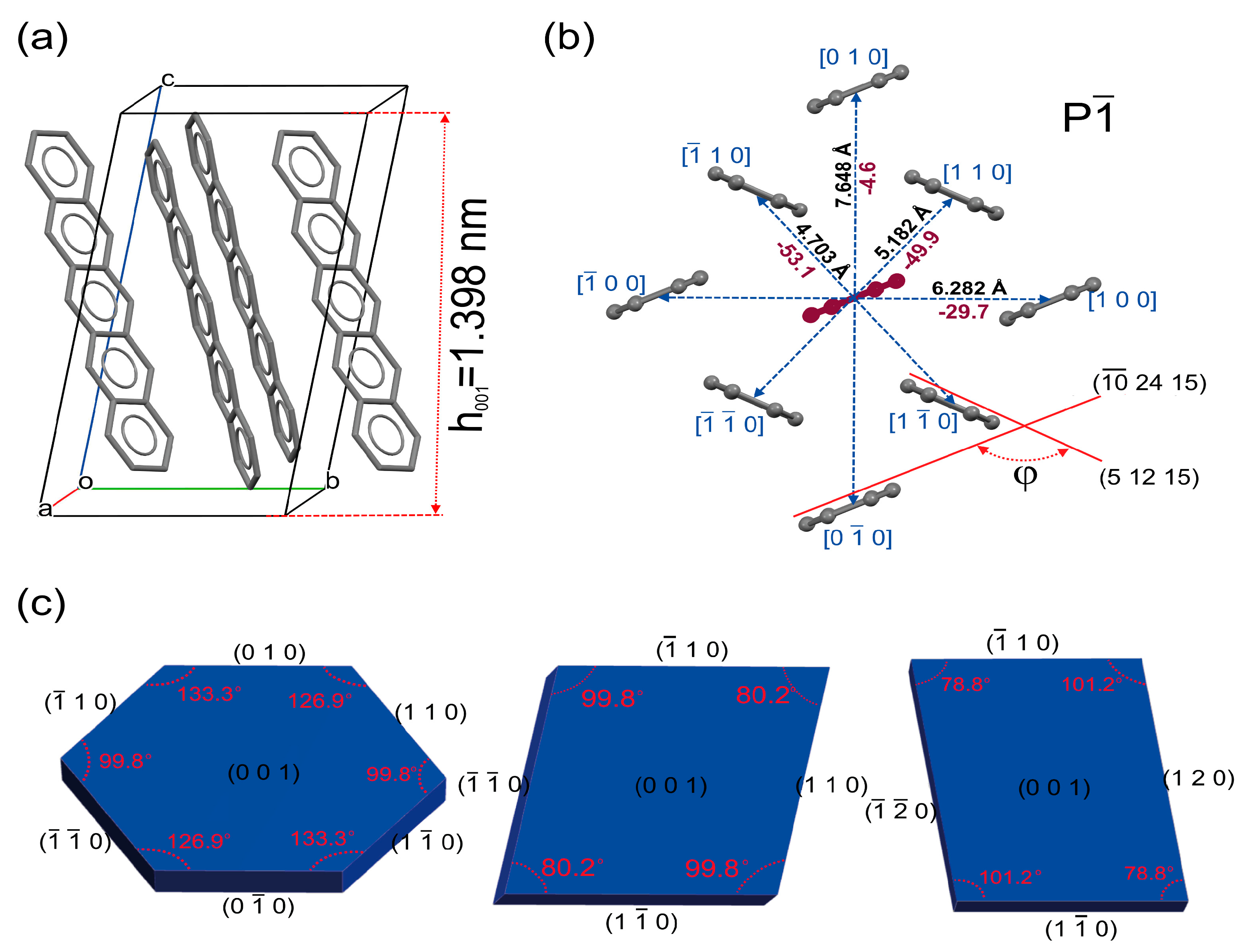
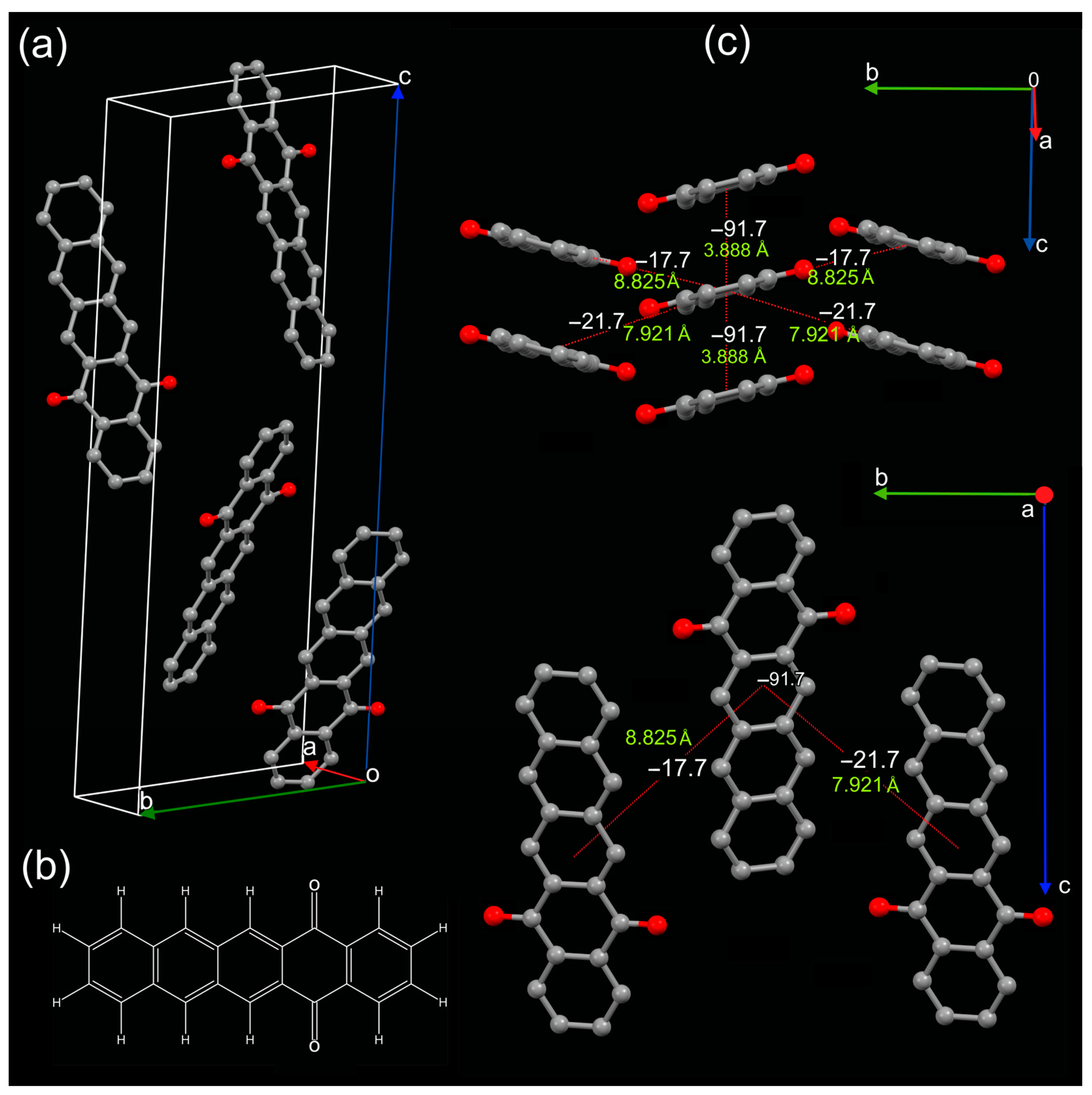
3.3. Crystal Structure and Morphology
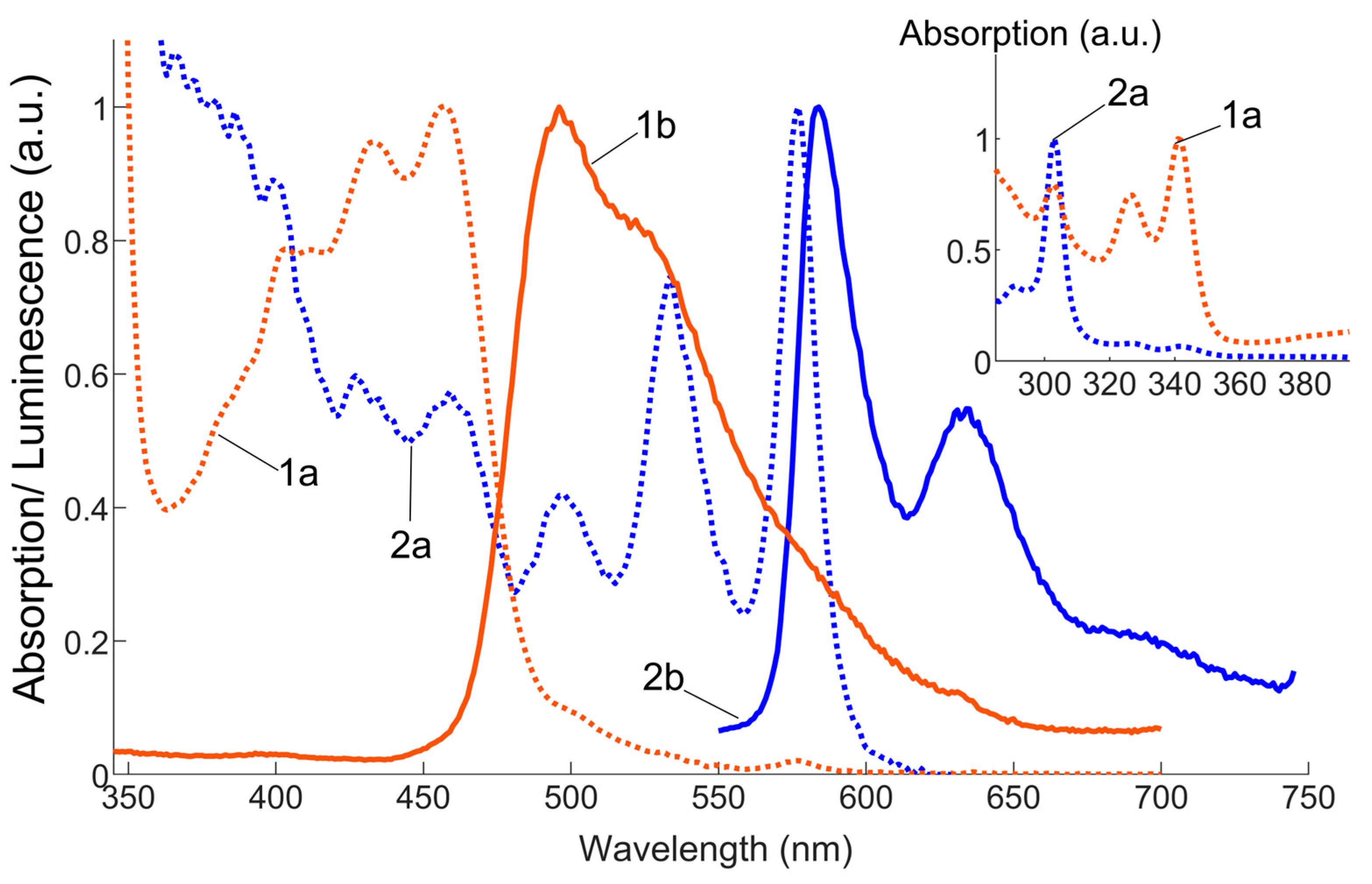
3.4. Optical Absorption and Luminescence Spectra
3.5. Electrical Properties
4. Conclusions
Supplementary Materials
Author Contributions
Funding
Data Availability Statement
Acknowledgments
Conflicts of Interest
Appendix A
References
- Zhang, X.H.; Domercq, B.; Wang, X.; Yoo, S.; Kondo, T.; Wang, Z.L.; Kippelen, B. High-Performance Pentacene Field-Effect Transistors Using Al2O3 Gate Dielectrics Prepared by Atomic Layer Deposition (ALD). Org. Electron. 2007, 8, 718–726. [Google Scholar] [CrossRef]
- Yi, M.; Guo, J.; Li, W.; Xie, L.; Fan, Q.; Huang, W. High-Mobility Flexible Pentacene-Based Organic Field-Effect Transistors with PMMA/PVP Double Gate Insulator Layers and the Investigation on Their Mechanical Flexibility and Thermal Stability. RSC Adv. 2015, 5, 95273–95279. [Google Scholar] [CrossRef]
- Kang, B.; Jang, M.; Chung, Y.; Kim, H.; Kwak, S.K.; Oh, J.H.; Cho, K. Enhancing 2D Growth of Organic Semiconductor Thin Films with Macroporous Structures via a Small-Molecule Heterointerface. Nat. Commun. 2014, 5, 4752. [Google Scholar] [CrossRef] [PubMed]
- Dong, J.; Yu, P.; Arabi, S.A.; Wang, J.; He, J.; Jiang, C. Enhanced Mobility in Organic Field-Effect Transistors Due to Semiconductor/Dielectric IInterface Control and Very Thin Single Crystal. Nanotechnology 2016, 27, 275202. [Google Scholar] [CrossRef] [PubMed]
- Kim, H.S.; Kim, S.; Koo, J.Y.; Choi, H.C. Highly Pure Pentacene Crystals Grown by Physical Vapor Transport: The Critical Role of the Carrier Gas. J. Mater. Chem. C 2021, 9, 1911–1917. [Google Scholar] [CrossRef]
- Ruiz, R.; Choudhary, D.; Nickel, B.; Toccoli, T.; Chang, K.C.; Mayer, A.C.; Clancy, P.; Blakely, J.M.; Headrick, R.L.; Iannotta, S.; et al. Pentacene Thin Film Growth. Chem. Mater. 2004, 16, 4497–4508. [Google Scholar] [CrossRef]
- Wang, H.; Li, F.; Gao, B.; Xie, Z.; Liu, S.; Wang, C.; Hu, D.; Shen, F.; Xu, Y.; Shang, H.; et al. Doped Organic Crystals with High Efficiency, Color-Tunable Emission toward Laser Application. Cryst. Growth Des. 2009, 9, 4945–4950. [Google Scholar] [CrossRef]
- Fan, C.L.; Lin, W.C.; Chang, H.S.; Lin, Y.Z.; Huang, B.R. Effects of the F4TCNQ-Doped Pentacene Interlayers on Performance Improvement of Top-Contact Pentacene-Based Organic Thin-Film Transistors. Materials 2016, 9, 46. [Google Scholar] [CrossRef]
- Kabakchiev, A.; Kuhnke, K.; Lutz, T.; Kern, K. Electroluminescence from Individual Pentacene Nanocrystals. ChemPhysChem 2010, 11, 3412–3416. [Google Scholar] [CrossRef]
- Zhao, Y.; Wang, L.; Chen, X.; Zhang, B.; Shen, F.; Song, H.; Wang, H. A High-Mobility, High-Luminescence and Low-Threshold Pentacene-Doped Cyano-Substituted Distyrylbenzene Crystal. J. Mater. Chem. C 2019, 7, 13447–13453. [Google Scholar] [CrossRef]
- Takeyama, Y.; Maruyama, S.; Matsumoto, Y. Growth of Single-Crystal Phase Pentacene in Ionic Liquids by Vacuum Deposition. Cryst. Growth Des. 2011, 11, 2273–2278. [Google Scholar] [CrossRef]
- Kulishov, A.A.; Yurasik, G.A.; Grebenev, V.V.; Postnikov, V.A. Tetracene Crystals: Growth from Solutions, Solubility, and Thermal Properties. Crystallogr. Rep. 2022, 67, 1001–1012. [Google Scholar] [CrossRef]
- Mattheus, C.C.; Dros, A.B.; Baas, J.; Meetsma, A.; De Boer, J.L.; Palstra, T.T.M. Polymorphism in Pentacene. Acta Cryst. C 2001, 57, 939–941. [Google Scholar] [CrossRef] [PubMed]
- Kim, S.H.; Jang, M.; Yang, H.; Park, C.E. Effect of Pentacene-Dielectric Affinity on Pentacene Thin Film Growth Morphology in Organic Field-Effect Transistors. J. Mater. Chem. 2010, 20, 5612–5620. [Google Scholar] [CrossRef]
- Yang, X.; Li, M.; Maeno, A.; Yanase, T.; Yokokura, S.; Nagahama, T. Growth of Pentacene Crystals by Naphthalene Flux Method. ACS Omega 2022, 7, 28618–28623. [Google Scholar] [CrossRef] [PubMed]
- Lee, J.Y.; Roth, S.; Park, Y.W. Anisotropic Field Effect Mobility in Single Crystal Pentacene. Appl. Phys. Lett. 2006, 88, 252106. [Google Scholar] [CrossRef]
- Laudise, R.; Kloc, C.; Simpkins, P.G.; Siegrist, T. Physical Vapor Growth of Organic Semiconductors. J. Cryst. Growth 1998, 187, 449–454. [Google Scholar] [CrossRef]
- Roberson, L.B.; Kowalik, J.; Tolbert, L.M.; Kloc, C.; Zeis, R.; Chi, X.; Fleming, R.; Wilkins, C. Pentacene Disproportionation during Sublimation for Field-Effect Transistors. J. Am. Chem. Soc. 2005, 127, 3069–3075. [Google Scholar] [CrossRef]
- Jo, S.; Takenaga, M. Morphologies of Pentacene Crystals Obtained by Physical Vapor Growth Technique. Jpn. J. Appl. Phys. 2010, 49, 078002. [Google Scholar] [CrossRef]
- Jo, S.; Kajiwara, K.; Takenaga, M. Growth Process of Pentacene Crystals Obtained by Physical Vapor Transport Technique. Jpn. J. Appl. Phys. 2014, 53, 115506. [Google Scholar] [CrossRef]
- Park, J.E.; Son, M.; Hong, M.; Lee, G.; Choi, H.C. Crystal-Plane-Dependent Photoluminescence of Pentacene 1da Wire and 2da Disk Crystals. Angew. Chemie 2012, 124, 6489–6494. [Google Scholar] [CrossRef]
- Chen, K.Y.; Hsieh, H.H.; Wu, C.C.; Hwang, J.J.; Chow, T.J. A New Type of Soluble Pentacene Precursor for Organic Thin-Film Transistors. Chem. Com. 2007, 10, 1065–1067. [Google Scholar] [CrossRef]
- Fulem, M.; Laštovka, V.; Straka, M.; Růžička, K.; Shaw, J.M. Heat Capacities of Tetracene and Pentacene. J. Chem. Eng. Data 2008, 53, 2175–2181. [Google Scholar] [CrossRef]
- Postnikov, V.A.; Sorokina, N.I.; Lyasnikova, M.S.; Kulishov, A.A.; Voloshin, A.E.; Borshchev, O.V.; Surin, N.M.; Svidchenko, E.A.; Ponomarenko, S.A. Large Area Free-Standing Single Crystalline Films of p-Quinquephenyl: Growth, Structure and Photoluminescence Properties. Crystals 2020, 10, 363. [Google Scholar] [CrossRef]
- Okada, Y.; Uno, M.; Nakazawa, Y.; Sasai, K.; Matsukawa, K.; Yoshimura, M.; Kitaoka, Y.; Mori, Y.; Takeya, J. Low-Temperature Thermal Conductivity of Bulk and Film-like Rubrene Single Crystals. Phys. Rev. B Condens. Matter Mater. Phys. 2011, 83, 113305. [Google Scholar] [CrossRef]
- Ma, L.; Zhang, K.; Kloc, C.; Sun, H.; Michel-Beyerle, M.E.; Gurzadyan, G.G. Singlet Fission in Rubrene Single Crystal: Direct Observation by Femtosecond Pump-Probe Spectroscopy. Phys. Chem. Chem. Phys. 2012, 14, 8307–8312. [Google Scholar] [CrossRef]
- Park, C.; Park, J.E.; Choi, H.C. Crystallization-Induced Properties from Morphology-Controlled Organic Crystals. Acc. Chem. Res. 2014, 47, 2353–2364. [Google Scholar] [CrossRef]
- Courté, M.; Ye, J.; Jiang, H.; Ganguly, R.; Tang, S.; Kloc, C.; Fichou, D. Tuning the π-π Overlap and Charge Transport in Single Crystals of an Organic Semiconductor: Via Solvation and Polymorphism. Phys. Chem. Chem. Phys. 2020, 22, 19855–19863. [Google Scholar] [CrossRef] [PubMed]
- Gwiddion, version 2.59; Software for scanning probe microscopy data visualization and analysis; Czech Metrology Institute: Jihlava, Czech, 2020.
- CrysAlisPro, version 171.41_64.88a; Software for single crystal X-ray diffraction; Rigaku Corporation: Tokyo, Japan, 2018.
- Petrícek, V.; Dušek, M.; Palatinus, L. Crystallographic Computing System JANA2006: General Features. Zeitschrift Krist. 2014, 229, 342–345. [Google Scholar]
- Palatinus, L. Ab Initio Determination of Incommensurately Modulated Structures by Charge Flipping in Superspace. Acta Cryst. A 2004, 60, 604–610. [Google Scholar] [CrossRef]
- Mercury, version 2022.2.0; Software for Crystal Structure Visualization, Exploration and Analysis; The Cambridge Crystallographic Data Centre: Cambridge, UK, 2022.
- Gavezzotti, A. Are Crystal Structures Predictable? Acc. Chem. Res. 1994, 27, 309–314. [Google Scholar] [CrossRef]
- Tsumura, A.; Koezuka, H.; Ando, T. Macromolecular Electronic Device: Field-Effect Transistor with a Polythiophene Thin Film. Appl. Phys. Lett. 1986, 49, 1210–1212. [Google Scholar] [CrossRef]
- Campbell, R.B.; Robertson, J.M.; Trotter, J. The Crystal Structure of Hexacene, and a Revision of the Crystallographic Data for Tetracene. Acta Cryst. 1962, 15, 289. [Google Scholar] [CrossRef]
- Schiefer, S.; Huth, M.; Dobrinevski, A.; Nickel, B. Determination of the Crystal Structure of Substrate-Induced Pentacene Polymorphs in Fiber Structured Thin Films. J. Am. Chem. Soc. 2007, 129, 10316–10317. [Google Scholar] [CrossRef]
- Chernov, A.A. Madern Crystallography III: Crystal Growth; Springer: Berlin/Heidelberg, Germany, 1984; ISBN 978-3-642-81837-0. [Google Scholar]
- Haas, S.; Batlogg, B.; Besnard, C.; Schiltz, M.; Kloc, C.; Siegrist, T. Large Uniaxial Negative Thermal Expansion in Pentacene Due to Steric Hindrance. Phys. Rev. B Condens. Matter Mater. Phys. 2007, 76, 205203. [Google Scholar] [CrossRef]
- Yanase, T.; Tanoguchi, H.; Sakai, N.; Jin, M.; Yamane, I.; Kato, M.; Ito, H.; Nagahama, T.; Shimada, T. Single Crystal Growth of π-Conjugated Large Molecules without Solubilizing Alkyl Chains via the Naphthalene Flux Method. Cryst. Growth Des. 2021, 21, 4683–4689. [Google Scholar] [CrossRef]
- Postnikov, V.A.; Lyasnikova, M.S.; Kulishov, A.A.; Sorokina, N.I.; Voloshin, A.E.; Skorotetcky, M.S.; Borshchev, O.V.; Ponomarenko, S.A. Growth Anisotropy and Crystal Structure of Linear Conjugated Oligomers. Phys. Solid State 2019, 61, 2322–2325. [Google Scholar] [CrossRef]
- Kaminsky, W. From CIF to Virtual Morphology Using the WinXMorph Program. J. Appl. Cryst. 2007, 40, 382–385. [Google Scholar] [CrossRef]
- Laduranty, J.; Lepage, L.; Lepage, Y. Capture Du Paradiméthoxyorthoquinodiméthane: Synthèses de Quinones et d’un Intermédiaire de La Daunomycinone. Can. J. Chem. 1980, 58, 1161–1167. [Google Scholar] [CrossRef]
- Smith, J.G.; Dibble, P.W.; Sandborn, R.E. The Preparation and Reactions of Naphtho[l,2-c]Furan and Naphtho[2,3-c ]Furan. J. Org. Chem. 1986, 51, 3762–3768. [Google Scholar] [CrossRef]
- Nishina, Y.; Kida, T.; Ureshino, T. Facile Sc(OTf)3-Catalyzed Generation and Successive Aromatization of Isobenzofuran from o -Dicarbonylbenzenes. Org. Lett. 2011, 13, 3960–3963. [Google Scholar] [CrossRef] [PubMed]
- Postnikov, V.A.; Sorokina, N.I.; Kulishov, A.A.; Lyasnikova, M.S.; Grebenev, V.V.; Voloshin, A.E.; Borshchev, O.V.; Skorotetcky, M.S.; Surin, N.M.; Svidchenko, E.A.; et al. Highly Luminescent Crystals of a Novel Linear π-Conjugated Thiophene-Phenylene Co-Oligomer with a Benzothiadiazole Fragment. Acta Cryst. B 2019, 75, 1076–1085. [Google Scholar] [CrossRef] [PubMed]
- Postnikov, V.A.; Sorokina, N.I.; Kulishov, A.A.; Lyasnikova, M.S.; Sorokin, T.A.; Freidzon, A.Y.; Stepko, A.S.; Borshchev, O.V.; Skorotetsky, M.S.; Surin, N.M.; et al. A New Linear Phenyloxazole–Benzothiadiazole Luminophore: Crystal Growth, Structure and Fluorescence Properties. Acta Cryst. B 2022, 78, 261–269. [Google Scholar] [CrossRef]
- Hellner, C.; Lindqvist, L.; Roberge, P.C. Absorption Spectrum and Decay Kinetics of Triplet Pentacene in Solution, Studied by Flash Photolysis. J. Chem. Soc., Faraday Trans. 2 1972, 68, 1928–1937. [Google Scholar] [CrossRef]
- Shimizu, A.; Ito, A.; Teki, Y. Photostability Enhancement of the Pentacene Derivative Having Two Nitronyl Nitroxide Radical Substituents. Chem. Com. 2016, 52, 2889–2892. [Google Scholar] [CrossRef]


| Sample | I (Dark-Blue) | II (Golden) |
|---|---|---|
| Formula | C22H14 | C22H12O2 |
| Temperature (K) | 85 | 85 |
| Space group | P | P212121 |
| Z | 2 | 4 |
| a (Å) | 6.2818 (1) | 3.88783 (4) |
| b (Å) | 7.6478 (1) | 12.4001 (0) |
| c (Å) | 14.3514 (2) | 28.9907 (8) |
| α (°) | 76.958 (1) | 90 |
| β (°) | 88.278 (1) | 90 |
| γ (°) | 84.339 (1) | 90 |
| V (Å3) | 668.39 (2) | 1397.62 (15) |
| Mr | 278.4 | 308.3 |
| DX (g/cm3) | 1.383 | 1.465 |
| µ (mm−1) | 0.078 | 0.093 |
| Radiation; λ (Å) | MoKα; 0.71069 | |
| Diffractometer | four-circle diffractometer XtaLAB Synergy R, DW system, HyPix-Arc 150 Hybrid Pixel Array Detector | |
| Scan type | ω | |
| Absorption correction; Tmin/Tmax | 0.557/1.000 | 0.844/1.000 |
| Θmax (°) | 48.67 | 48.78 |
| No. of measured, independent, and observed [I > 3σ(I)] reflections | 57,330, 6730, 5282 | 114,915, 2267, 1537 |
| Rint | 0.015 | 0.15 |
| R/wR | 0.024/0.031 | 0.055/0.052 |
| S | 1.83 | 2.15 |
| Δρmin/Δρmax (e·Å−3) | −0.19/0.25 | −0.21/0.54 |
| Active Layer | Ref. | Dielectric | Layer Thickness (nm) | <dgr> (nm) | W/L | μsat (<μsat>) (cm2·V−1s−1) | <VT> (V) |
|---|---|---|---|---|---|---|---|
| polycrystalline film (initial) | this work | SiO2 (440 nm) | 40 ± 10 | 130 | 10 | 0.01 (0.004 *) | −15 * |
| polycrystalline film (purified) | this work | SiO2 (440 nm) | 40 ± 10 | 180 | 5 | 0.07 (0.02 **) | −5 ** |
| [2] | PMMA/PVP (60 nm) | 50 | - | 20 | 1.51 | −20.1 | |
| Si/SiO2 (300 nm)/OTS | 50 | - | 20 | 0.66 | −12.3 | ||
| Single crystal | this work | SiO2 (440 nm) + PMMA (290 nm) | 2300 ± 100 | - | 10 | 0.40 (0.10 ***) | −8 *** |
| [3] | - | 45 | - | - | 6.2 (5.5) | −37.5 | |
| [4] | - | 30–300 | - | - | 5.7 (2.0) | - |
Disclaimer/Publisher’s Note: The statements, opinions and data contained in all publications are solely those of the individual author(s) and contributor(s) and not of MDPI and/or the editor(s). MDPI and/or the editor(s) disclaim responsibility for any injury to people or property resulting from any ideas, methods, instructions or products referred to in the content. |
© 2023 by the authors. Licensee MDPI, Basel, Switzerland. This article is an open access article distributed under the terms and conditions of the Creative Commons Attribution (CC BY) license (https://creativecommons.org/licenses/by/4.0/).
Share and Cite
Postnikov, V.A.; Kulishov, A.A.; Yurasik, G.A.; Sorokina, N.I.; Sorokin, T.A.; Grebenev, V.V. Growth and Characterization of Centimeter-Scale Pentacene Crystals for Optoelectronic Devices. Crystals 2023, 13, 999. https://doi.org/10.3390/cryst13070999
Postnikov VA, Kulishov AA, Yurasik GA, Sorokina NI, Sorokin TA, Grebenev VV. Growth and Characterization of Centimeter-Scale Pentacene Crystals for Optoelectronic Devices. Crystals. 2023; 13(7):999. https://doi.org/10.3390/cryst13070999
Chicago/Turabian StylePostnikov, Valery A., Artem A. Kulishov, Georgy A. Yurasik, Nataliya I. Sorokina, Timofei A. Sorokin, and Vadim V. Grebenev. 2023. "Growth and Characterization of Centimeter-Scale Pentacene Crystals for Optoelectronic Devices" Crystals 13, no. 7: 999. https://doi.org/10.3390/cryst13070999
APA StylePostnikov, V. A., Kulishov, A. A., Yurasik, G. A., Sorokina, N. I., Sorokin, T. A., & Grebenev, V. V. (2023). Growth and Characterization of Centimeter-Scale Pentacene Crystals for Optoelectronic Devices. Crystals, 13(7), 999. https://doi.org/10.3390/cryst13070999