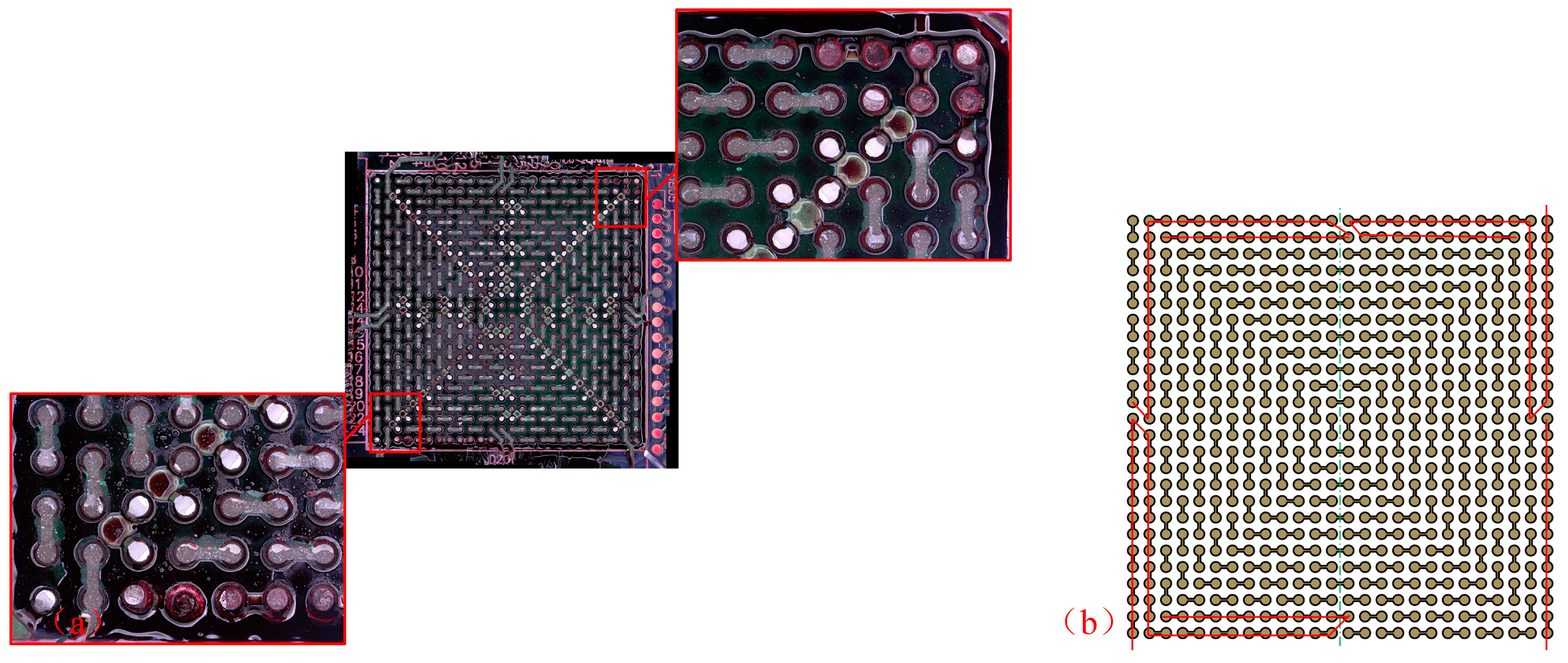
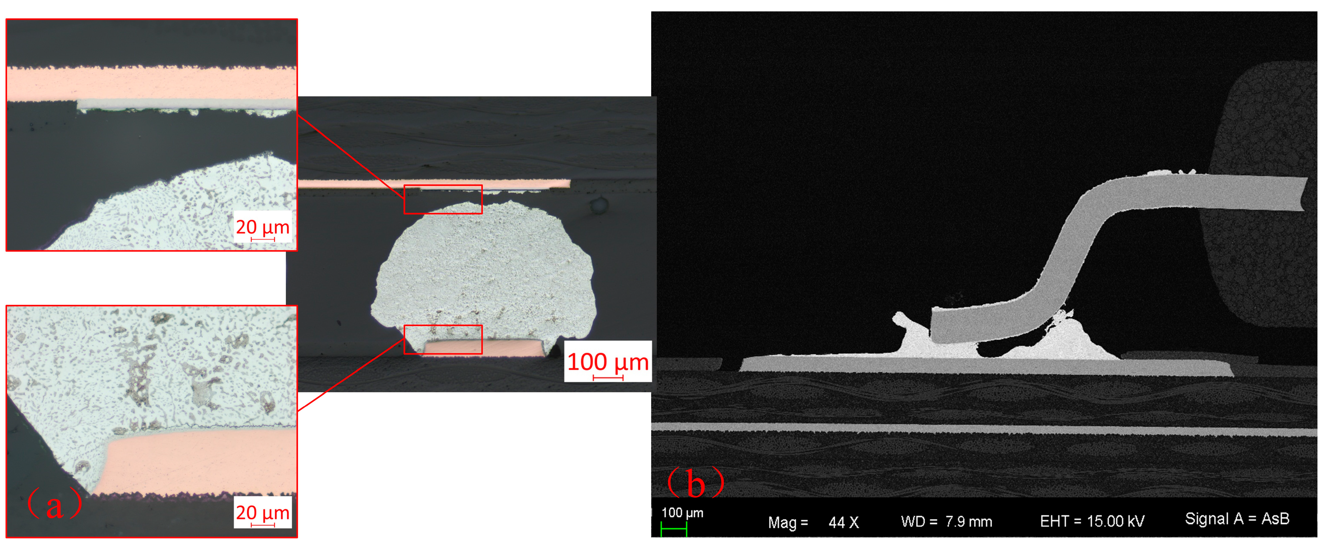
Abstract
The electronic devices suffer great vibration and temperature fluctuation in an airborne environment, which has been always a big challenge for reliability design. In this paper, the reliability of the complex electronic components for airborne applications under a thermal cycling test, random vibration and combined loading has been investigated by experiment tests and finite element simulation. The fatigue life and failure location under different loadings have been compared and discussed, respectively. The results indicated that the combined fatigue life was much shorter than a single-factor experiment. The failed solder joints mostly appeared at the interface between the solder and the copper pad on the component side and the location was at the corner for all three harsh environment tests. Nevertheless, several differences could be observed. For temperature cycling, all the specimens failed due to the increase in daisy chain resistance rather than the open circuit for the combined loading test. That is because the degeneration of the solder caused by temperature variation led to lower stress levels and fatigue life. Moreover, the pins fractured at the welding regions have been observed. The modified Coffin—Manson model, Miner’s linear fatigue damage criterion and Steinberg’s model and rapid life-prediction approach were used to predict the fatigue life under temperature cycling, random vibration and combined loading, respectively. With these methods, the accurate numerical models could be developed and validated by experiment results. Thanks to the simulation, the design time could be effectively shortened and the weak point could be determined.
1. Introduction
Airborne electronic equipment often suffers harsher conditions than standard commercial devices, including rapidly changing temperatures and severe vibration environments, which is a tremendous challenge to reliability design for microelectronic industries [1,2]. In general, 52% of the failures of airborne electronic devices are mainly caused by environmental effects, of which 42% are caused by temperature, 27% by vibration and 19% by humidity according to the U.S. air force statistics. It could be seen that temperature and vibration load have the most significant impact on the reliability of airborne components. However, with the development of advanced packaging technology, traditional two-dimensional (2D) packaging technologies have gradually converted to advanced three-dimensional (3D) packaging with far higher interconnect density, higher power, and smaller size [3,4]. These factors would further lead to reliability problems for the devices. The concerns are mostly related to the failure of the interconnected parts, especially for the solder joint [5,6,7]. The increased resistance, even a broken circuit caused by a harsh environment, could lead to severe reliability problems [8].
The reliability of solder joints under thermal cycles has been the subject of many studies. For instance, Emeka H. Amalu et al. reported an investigation on the high-temperature reliability of a model flip chip package assembled on a substrate-printed circuit board. He found that the thickness of IMC affected the reliability and service life of the solder bump joints, which observed high-temperature excursions, such that very thin and very thick IMC increased the damage to the solder bump joints [9]. Hiroki Kanai et al. proposed that in die-attach joints, fatigue crack networks formed by equibiaxial stresses are continuously initiating and propagating crisscross-shaped cracks. High-speed thermal cycling generates stresses and accelerates crack initiation as the cycle advances [10]. Liu et al. used the multiscale interface element method to evaluate the chip scale package’s interfacial peel and shear stress distributions. The proposed method displayed the accuracy of analyzing structural singularities in the thermal stress distribution of the chip scale during the thermal cycle process [11]. Pan et al. studied the effect of thermal shock on the solder joint shear strength and IMC thickness. He pointed out that the thermal shock led to a thicker and smoother IMC layer. Moreover, thermal shock and thermal aging did not differ significantly in terms of IMC thickness growth [12]. As a result of thermal shock tests, Kang et al. studied the degradation characteristics of solder joints. Ni3Sn4 IMCs were detected at the starting point of the shear fracture surface which influenced the shear force reduction and the forming shear surface [13]. Dalton et al. calculated the induced nominal strain of several kinds of solder joint material during thermomechanical fatigue. The strain induced by temperature cycling, coupled with the thermal exposure at the high end of the cycle, was responsible for driving the particle coarsening mechanisms. Meanwhile, higher strain levels led to accelerated fatigue failure of solder joints [14]. Wentlent et al. studied the effects of amplitude variations on deformation and damage evolution in the solder joints in thermal cycling. The density of the dislocation structures increased with increasing cycling amplitude. As a result of the variations in amplitude, the density was permanently enhanced, leading to damage and failure under continuing variations in amplitude [15].
Many factors affect the failure mechanisms of solder joints under mechanical vibration. Xia et al. proposed a novel methodology to predict the fatigue life of solder joints under random vibration loading by employing a vibration test. As the excitation level increased, the fatigue life of the assembled package-on-package significantly decreased. Furthermore, the solder joints for the 3D packaging were less durable than the 2D packaging because the stress level from the S-N curve was the smallest compared with other 2D packaging structures [16]. Baishya et al. studied the effects of vibration on the reliability of area array solder joints in an industry-grade printed circuit board (PCB). Two trigger points within the lifetime of a solder joint could be found, and the first one could be detected in crack initiation at around 35–40% of its lifetime, while the second trigger point indicated just before complete mechanical failure, tracked at around 80–85% of the lifetime [17]. Xia et al. studied the vibration reliability of lead-free solder joints of Package-on-Package and found that the cracks usually originated in the bottleneck position of the solder balls, extended within bulk solder, and then propagated along the interface between the IMC layer and the bulk solder under the vibration loading [18]. Kim et al. presented the finite element methods to analyze the stresses of the solder joints under vibration for satellite electronics devices applications. The solder stresses increased as the chip size increased, and the underfill remarkably enhanced the structural integrity and reduced the solder stresses [19]. Ding et al. conducted the microstructures and crack propagation behavior of ceramic column grid array solder joints under sinusoidal vibration loading, random vibration loading and thermal cycling. The cracks in the solder joints mainly occurred in the first two outermost rows. Meanwhile, PCB deformation during the mechanical vibrations brought a significant stress concentration at the peripheral solder joints and induced the initiation of cracks [20]. Ghaderi analyzed the solder joints’ fatigue life using the finite element method and tested it under different vibrations. The results showed that the fatigue effects result in the coalescence and the void growths in lower angles of vibration loadings. The peeling stresses and the displacement in the overall solder joints dramatically increase, along with the vibration frequencies for the higher amounts of the input power spectrum densities [21].
Researchers have mostly studied vibration and thermal cycles using tests and simulations up to now, but few researchers focused on the combined loading of vibration and thermal cycle. Further research is needed to determine the failure mechanisms of solder joints, especially for airborne applications with more harsh working conditions. The more accurate numerical models should be developed and proposed to reduce design costs and shorten the design period of products.
In this study, the fatigue life and failure mechanism under thermal cycling test, airborne level random vibration and combined loading were investigated by experiment tests and FEM simulation. The experimental method was prepared according to IPC-9701A guidelines, including defining failure criteria and selecting daisy chain test structures. In addition to the mean time to failure, a real-time viewing was performed. In order to determine the failure location and model, dye and pry tests, cross-section analysis and scanning electron microscopy (SEM) were used. A modified Coffin—Manson model, Miner’s linear fatigue damage criterion and Steinberg’s model and rapid life-prediction approach were introduced to calculate the thermal fatigue life, random vibration life and combined life, respectively. Full details of nomenclatures are given in Appendix A at the end of this article. Single loading and coupled loading were considered and results were discussed and compared. This paper can extend previous studies and help with the combined failure mechanism for solder joints for airborne applications. The proposed simulation method could be adopted to shorten the development cycle and cost savings.
2. Experimental Procedures and Simulation
2.1. Specimen and Testing
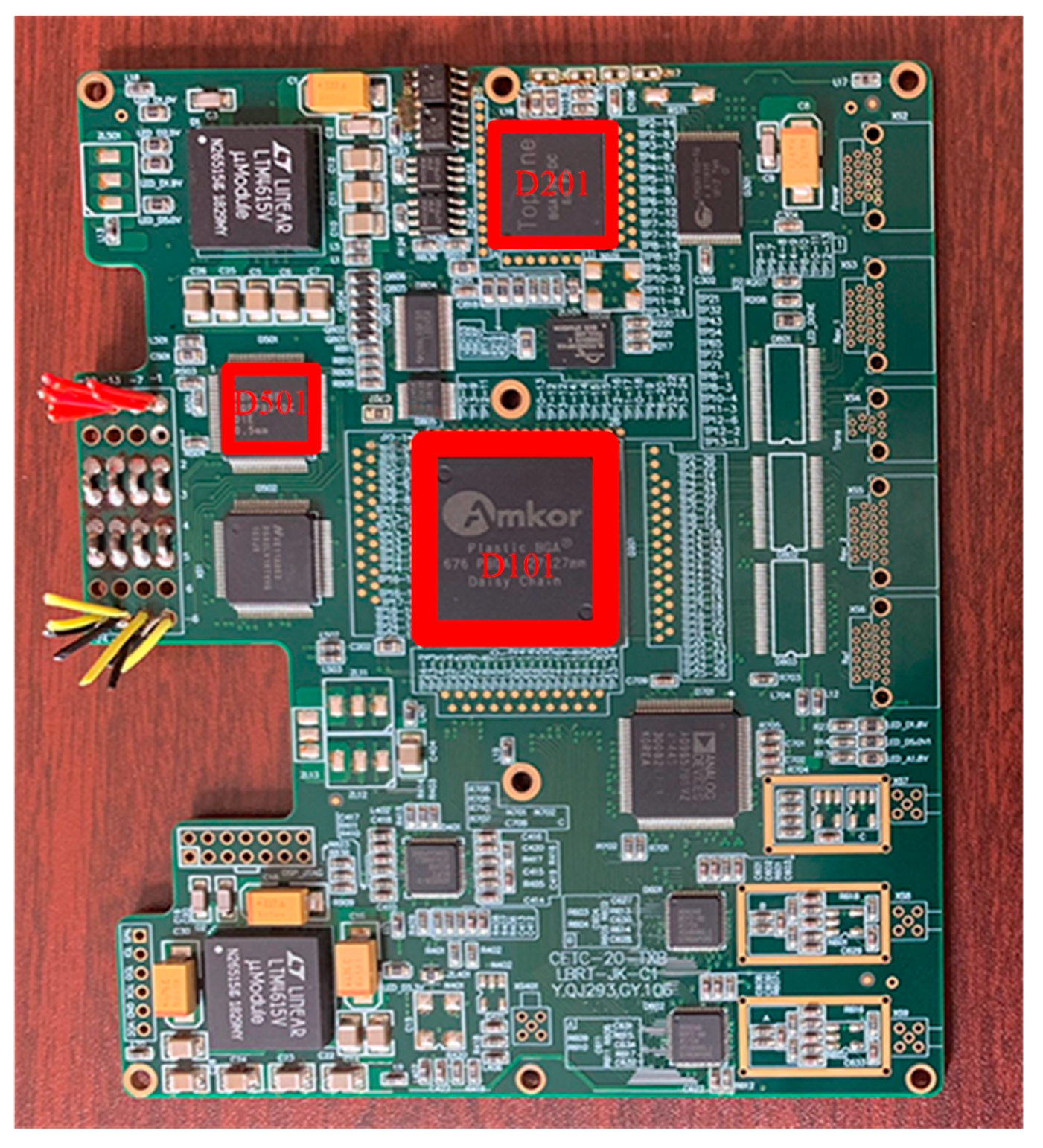
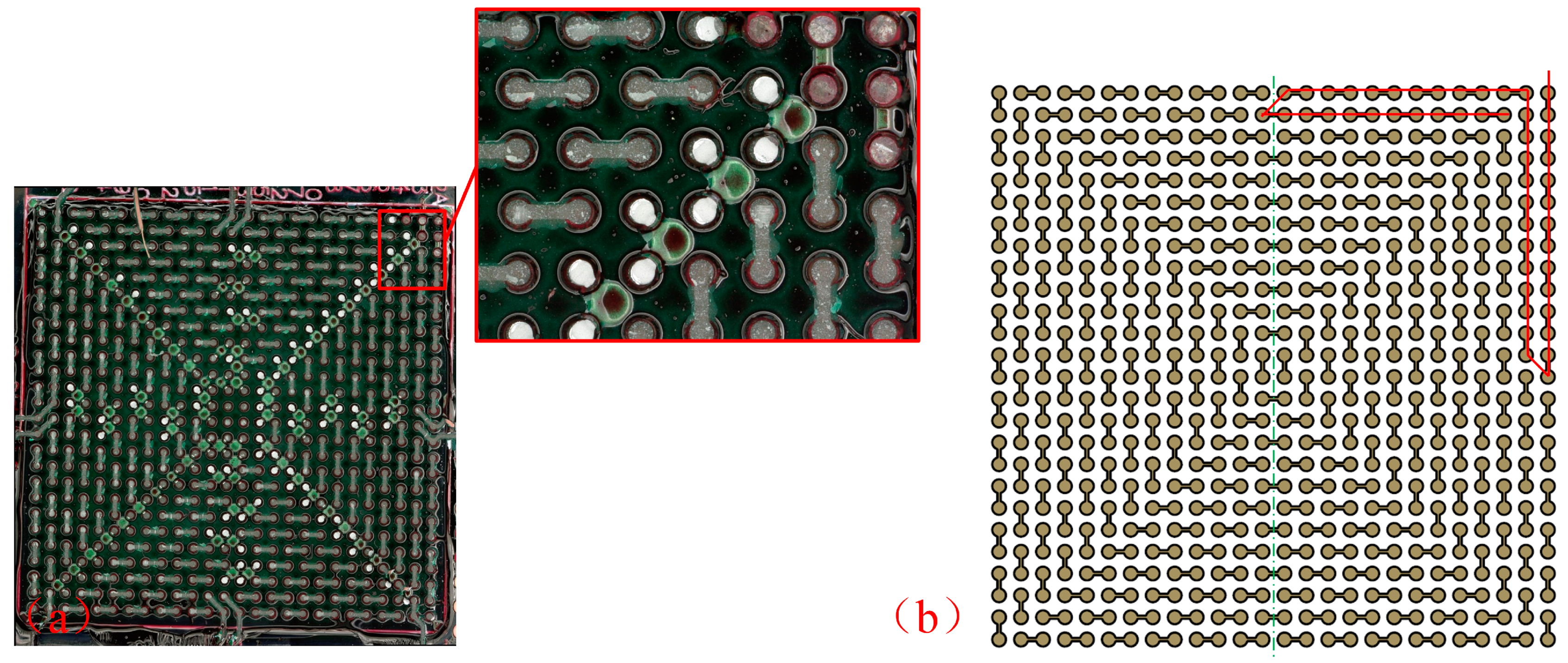
The specimen used in this paper was shown in Figure 1. The PCB was made of Flame Retardant 4 (FR4) with 135 mm × 110 mm × 2 mm. A daisy chain circuit, including two BGA devices (D101 and D201) and one QFP device (D501), was designed and manufactured to be constantly electrically monitored by an event detector and a data logger. Next, 63Sn37Pb, a typical material used widely for airborne applications, was used to assemble those components. The hot air heating method was applied to form the solder joints with a peak temperature of 245 °C. The time above liquidus temperatures was 97 s, preheating was 90 s between 100 °C and 120 °C, temperature rate before preheating was 3 °C/s, and the cooling rate was 3°C/s after melting.
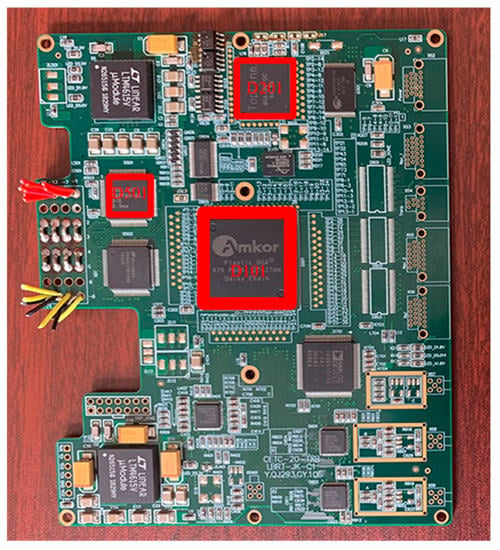
Figure 1.
Details of the specimen.
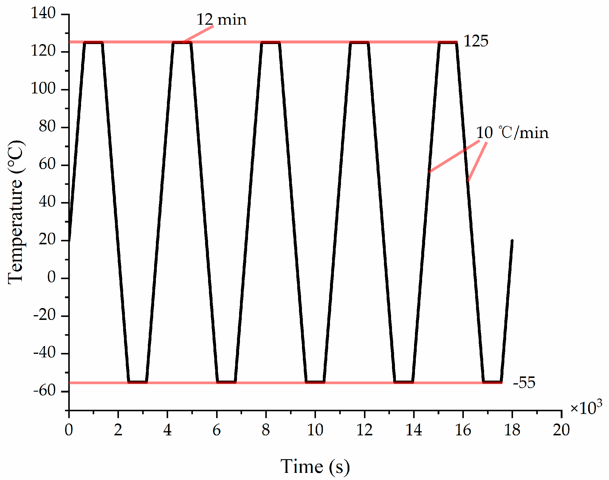
A temperature cycling test chamber was used to conduct a thermal cycle test. Figure 2 illustrated the temperature profile for the thermal cycle test. At the beginning of the experiment, the initial temperature was 20 °C, the maximum temperature was 125 °C, and the minimum temperature was −55 °C. Low dwell and high dwell were constant for 12 min, with a ramp of 10 °C per minute.
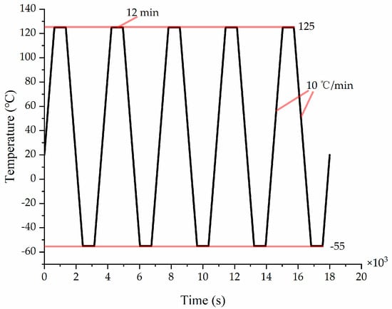
Figure 2.
Temperature cycling profile.
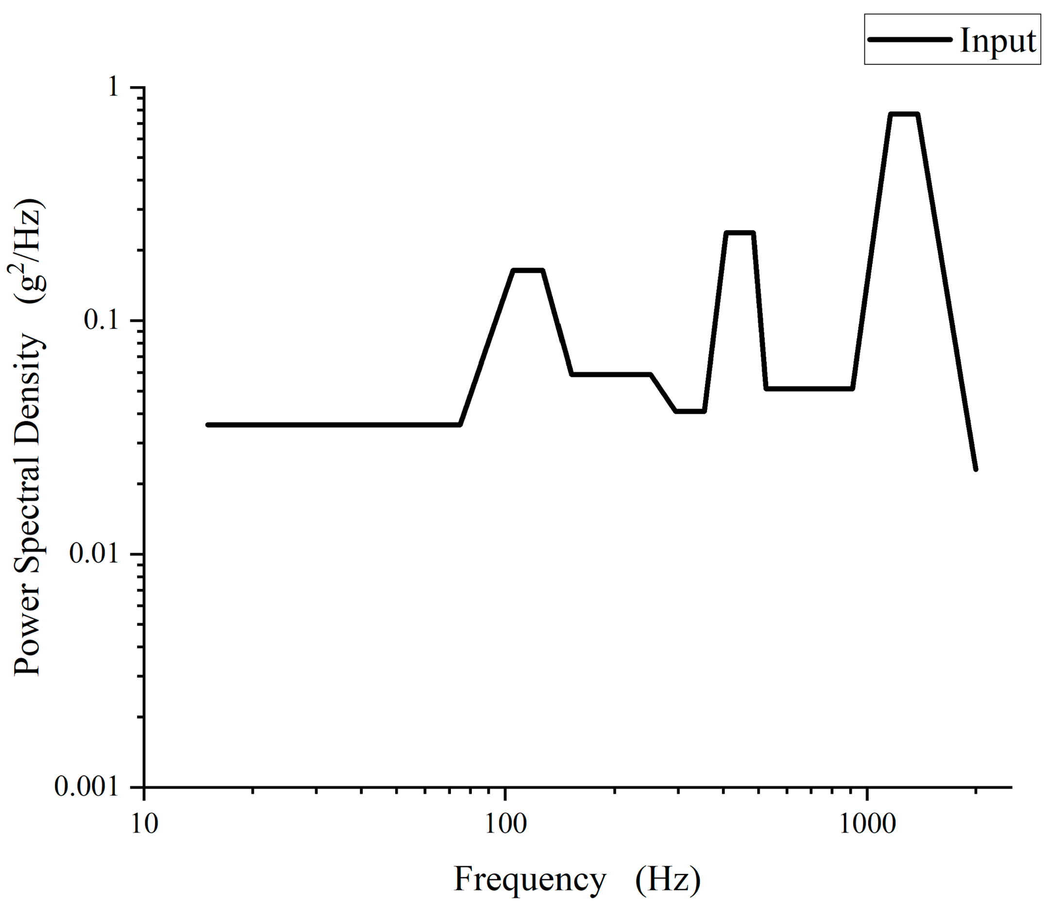
For random vibration, the power spectrums density (PSD) profile was shown in Figure 3 based on Table 1. This profile fully considered the vibration condition of electronic devices during flight. Table 1 showed the parameters of the random vibration profile used in this paper.
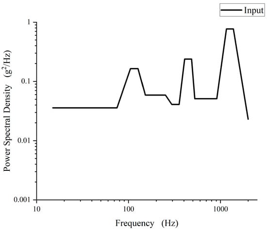
Figure 3.
Power density spectrums profile.

Table 1.
Parameters of the airborne level random vibration profile used in this paper root-mean-square acceleration = 20.64 g.
For both the random vibration and combined temperature-vibration, a combined temperature-vibration comprehensive test chamber was used to conduct the two tests. Meanwhile, the temperature and power density spectrums were simultaneously applied.
Furthermore, to perform the single random vibration and combined tests, the vehicles were mounted onto the shaker by all the eight corner screw holes in Figure 4. In order to characterize the system, two accelerometers were used to measure the input and output accelerations. To enhance the testing accuracy, typically 32 specimens were conducted for each test named by groups A, B and C, respectively. The data loggers were used to detect and record resistance change. Based on industry-standard IPC-9701A, failure definition could be described as a 20% nominal resistance increase in a daisy chain circuit. Similarly, fatigue life could be defined as when one-half of a given specimen has failed. So, the failure time of the 16th PCB was regarded as fatigue life. A failure analysis was conducted after the tests ended, followed by dye and pry tests on the prepared specimens. As part of this study, a cross-sectional analysis and high-resolution microscopy were conducted to identify the crack location and failure mode. All the instruments used in this paper were shown in Table 2.
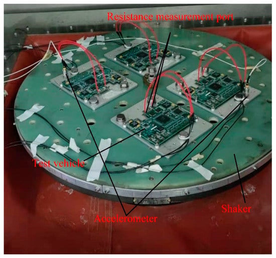
Figure 4.
Experiment set-up of single random vibration and combined tests.

Table 2.
Instruments used in this paper.
2.2. Simulation Approaches
A 3D finite element model of the test vehicle was developed using the commercial software ANSYS as shown in Figure 5. The dimensions of the model were the same as the test vehicle. Figure 6 showed the detail of the simulation model. The BGA device (D101 and D201) and one QFP device (D501) were the key daisy chain circuit devices which deserved focused attention and further analysis. The packaging structure parameters were listed in Table 3.
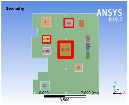
Figure 5.
The 3D finite element model.

Figure 6.
The finite element model of the key device: (a) D201, (b) D501.

Table 3.
Packaging structure parameters in FEA.
The model consisted of the Bismaleimide-Triazine (BT) substrate, Cu pad, solder joints, PCB and epoxy mold compound (EMC). All the devices can be equivalent to EMC except D101, D201 and D501. Based on the minimum energy principle, the solder shapes were simulated with surface evolver software, and then exported to ANSYS to perform finite element simulations.
Random vibration and transient structural module were used to calculate stresses and strains. The stresses and strains in this investigation were calculated under the assumption of an elastic response. Solid186 element which was high order three-dimensional solid structural element were used for simulation. All materials are considered elastic except the solder joints. In Table 4, all the material characteristics were reported including the materials of the component, density, Young’s modulus, Poisson’s ratio and coefficient of thermal expansion (CTE). Meanwhile, the non-linear mechanical properties of the solder were considered and characterized by the Anand viscoplastic constitutive model. The parameters of the Anand model for the solder joint were listed in Table 5.

Table 4.
The material parameters in FEA.

Table 5.
The parameters of the Anand model for the solder joint.
The total elements were 127,413, the number of nodes were 736,879 and the average element quality was 0.97321. The convergence of the model has been analyzed based on Modal analysis as shown in Table 6. A total of six mesh division methods were adopted which proved that the mesh division method used in this paper can not only ensure the analysis accuracy but also speed up the computing time.

Table 6.
The convergence analysis in this paper.
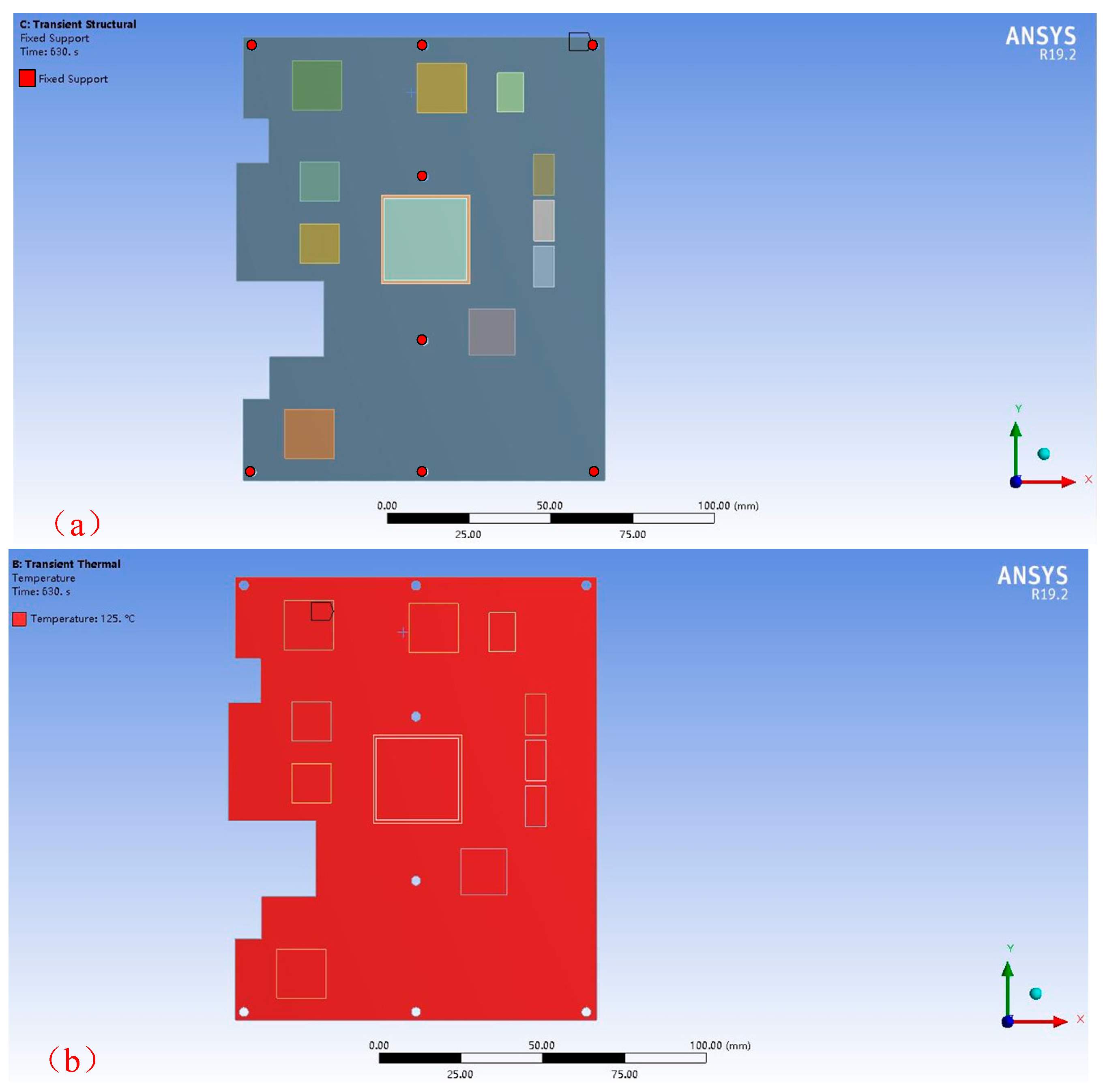
The same temperature cycling profile and power spectral density (PSD) profile of the excitation were applied in the finite element analysis, respectively. To create a robust stress-strain hysteresis loop for this temperature cycling profile, a total of five cycles were modeled. The boundary conditions were also exactly the same as the real test as shown in Figure 7.
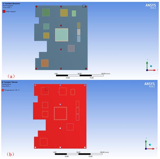
Figure 7.
Boundary conditions and loads: (a) the eight corner screw holes with fixed support; (b) temperature loads applied on all the external surface of the specimen.
In the combined temperature-vibration studies, the rapid life-prediction approach based on linear damage superposition was used in this paper. The random vibration damage estimations for each temperature level were calculated. The damage due to two different loadings was calculated using a generalized strain approach and superposed.
3. Results and Discussion
3.1. Temperature Cycling Test Analysis
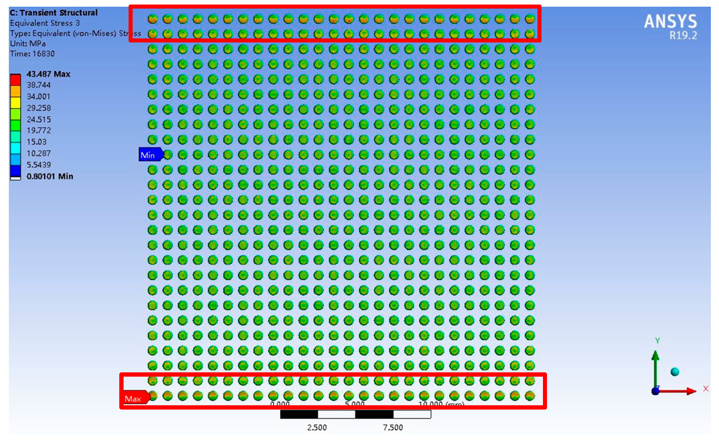
FEM calculated the thermal stress distribution under the thermal cycle test condition. The maximum equivalent stress appeared at the interface of the solder joints and copper electrode in D101. The von-Mises stress distribution during the stable cycle was shown in Figure 8. More stress was distributed along with the outer columns compared with the inner ones for solder joints. The solder joints at the corner were even more critical than the ones during the temperature cycling test. The maximum von-Mises stress was 43.487 MPa and it occurred at the low temperature stage which should be considered as the dangerous solder joint. On the contrary, the equivalent stress was much lower at the high temperature stage. This was because the solder material showed strong viscoplasticity at high temperature, and its deformation resistance and dynamic recovery characteristics were very low, so its thermal stress was very small. Then, the equivalent stress rose sharply as the temperature increased, indicating that the viscoplastic material had a process of re-cooling and hardening during the transition from high temperature to low temperature, resulting in its elastoplasticity decreasing and brittleness increasing.
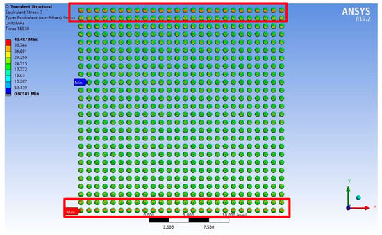
Figure 8.
The von-Mises stress distribution in D101.
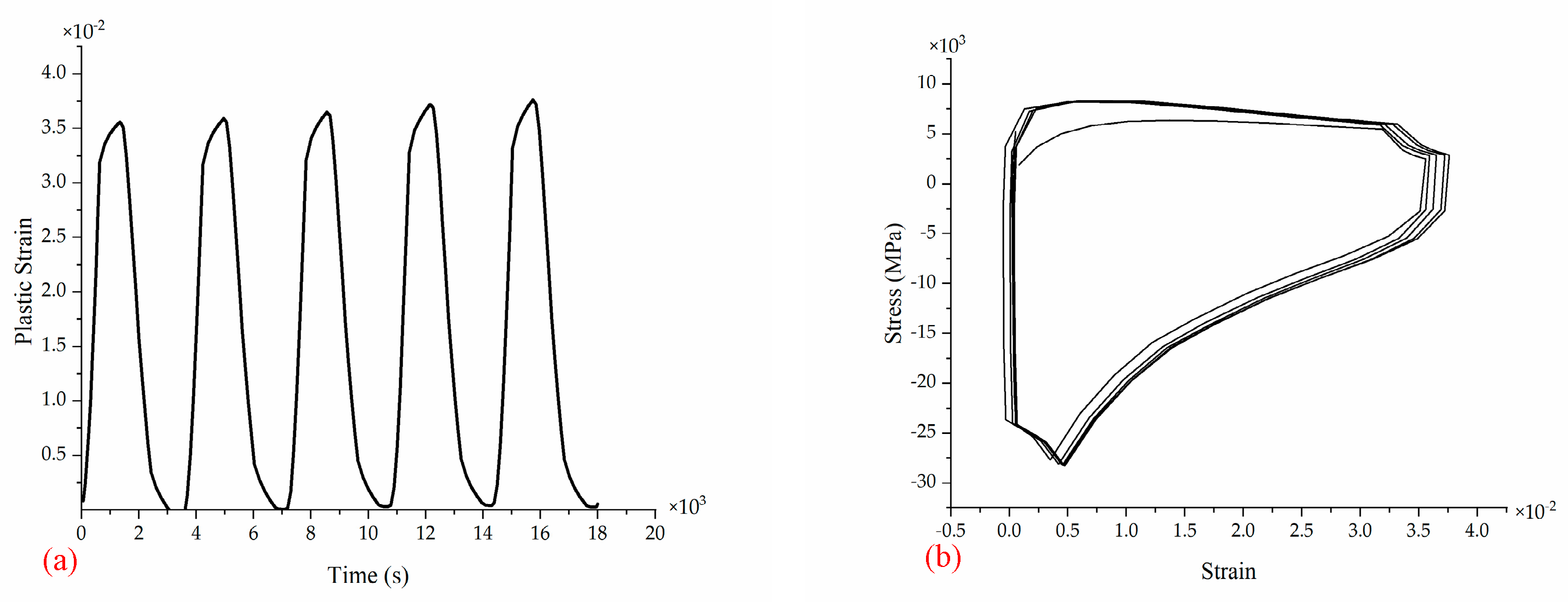
The mechanic response profile of the dangerous node of the solder joint was shown in Figure 9. As seen in Figure 9a, the maximum and minimum values of equivalent strain rise with each cycle, while the various values remained essentially the same. As shown in Figure 9b, it can be indicated that the accumulated plastic work remained stable and accumulated continuously until the critical value was reached; then, the solder joint failed as the enclosed area represented.
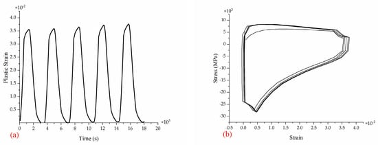
Figure 9.
The mechanic response profile: (a) the plastic strain curves of the dangerous solder node, (b) the stress-strain hysteresis loop of the dangerous solder node.
The modified Coffin—Manson based on plastic strain used for temperature cycling fatigue life prediction is listed as the following equation [22]:
where εf is the fatigue toughness coefficient, Nf is the fatigue lifetime of the thermal cycle, c is the fatigue toughness index, Δγp is the values of equivalent plastic strain calculated in a stable cycle by ANSYS. The following equation can be used to calculate the fatigue toughness index c:
Tm denotes the average temperature throughout the thermal cycle. f is the thermal cycle frequency in one day. Based on the simulation results, the max shear stress occurred in the YZ plane, and the equivalent plastic strain calculated in a stable cycle were 0.040325. A value of 527.9 h was calculated for the fatigue lifetime.
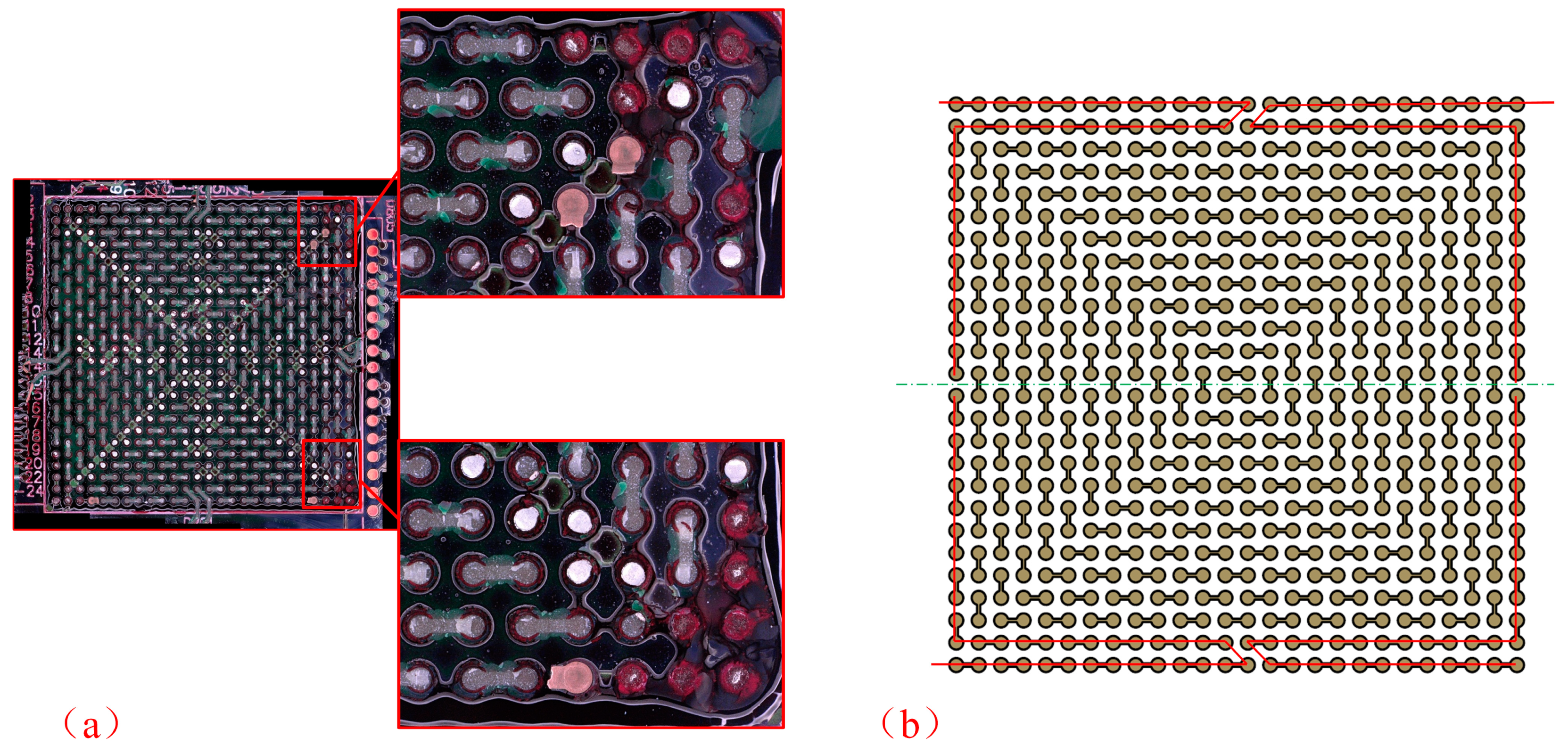
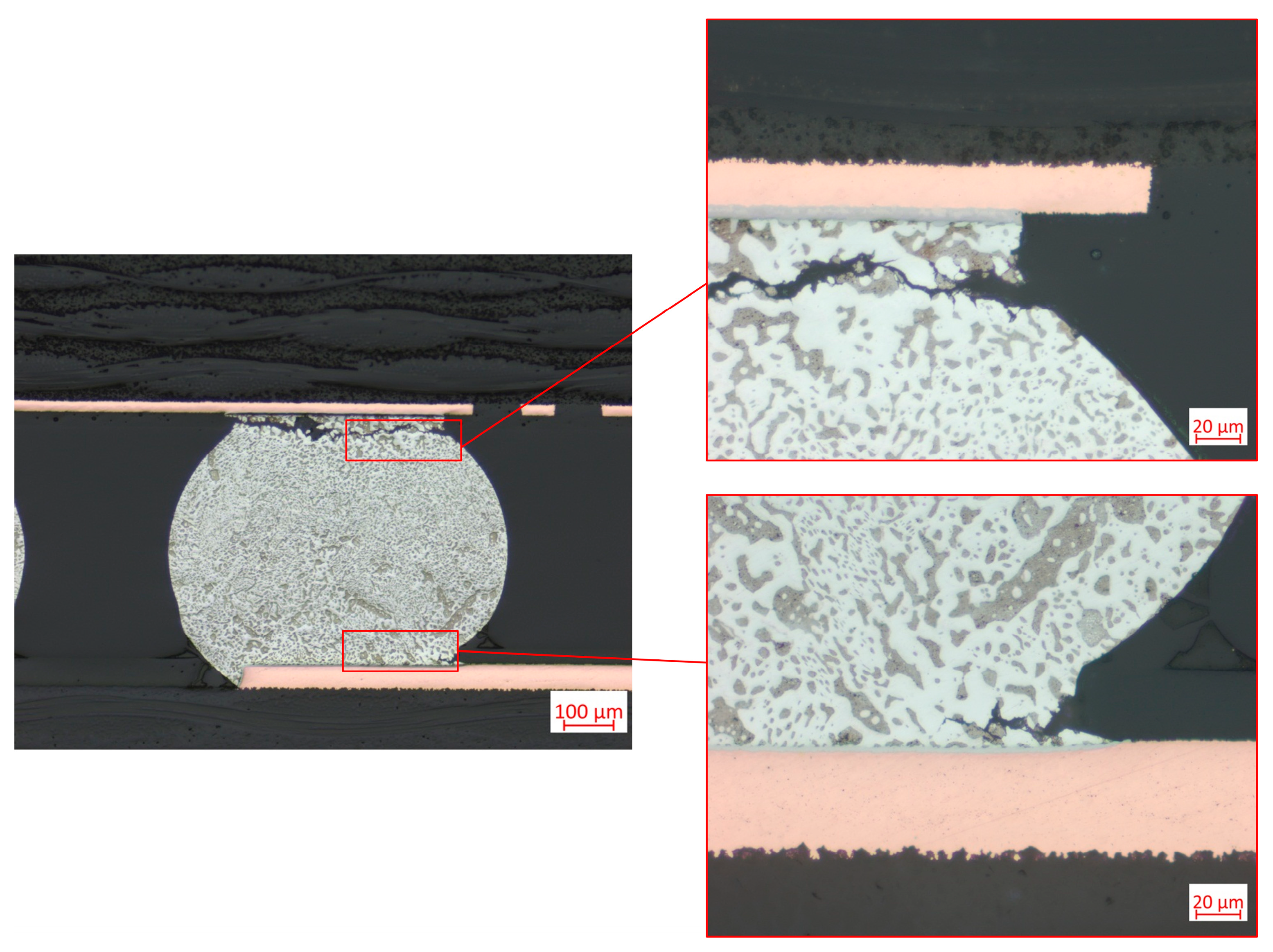
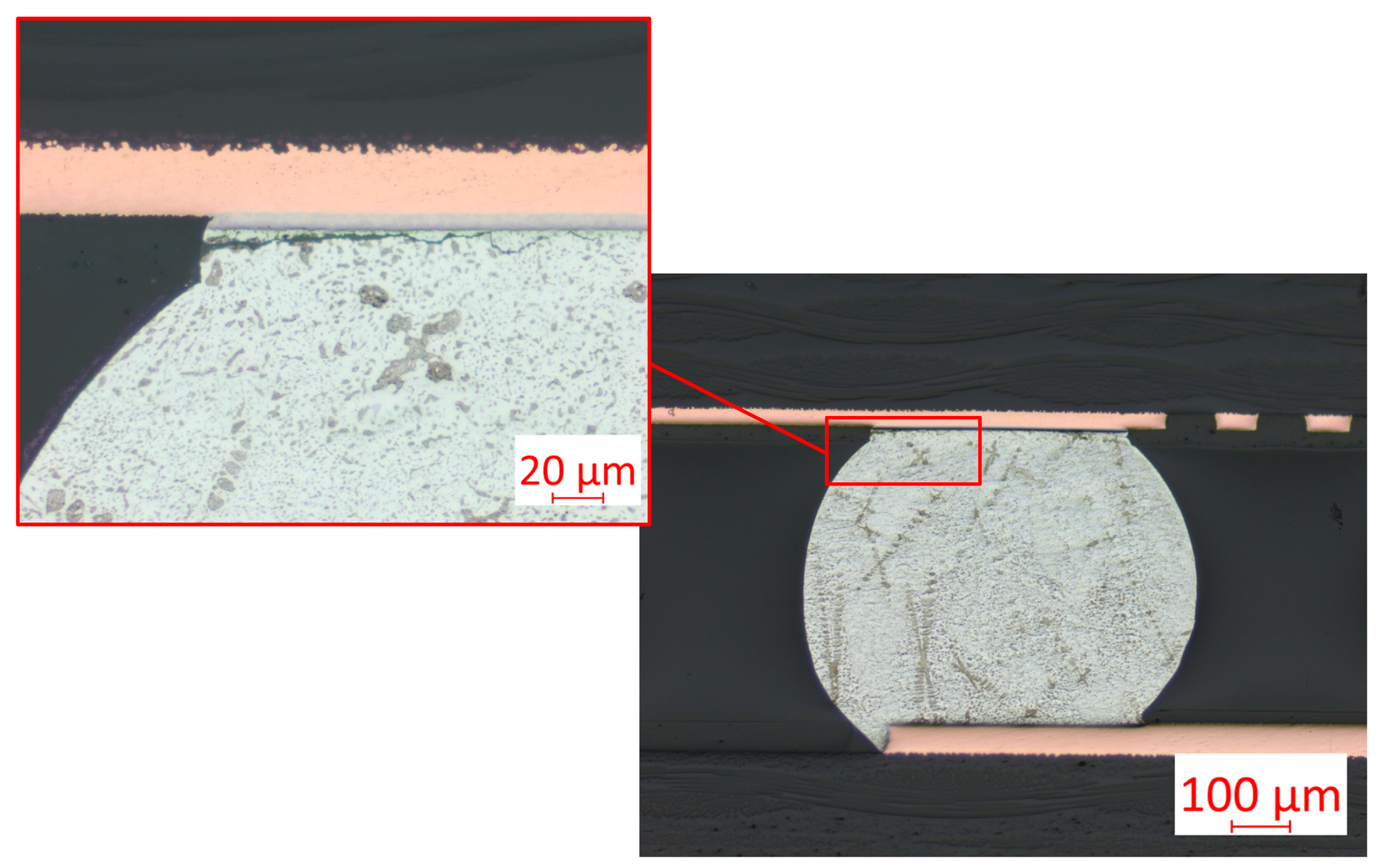
Figure 10 showed the dye and pry test results for the temperature cycling in D101. In the case of component D101, the failed solder joints appeared along the outer two columns, especially on the corners. The complete crack could be observed, as shown in Figure 11. On the component side, the fracture within the bulk solder was the typical failure mode to temperature cycling loading. At the same time, the small crack growth accelerated the fatigue life on the PCB side. This failure mode was partly due to the strength of the bulk solder being lower than the interface between the solder joint and the copper pad. Thermal mismatch induced by the interconnection structure greatly affected the growth of cracks of bulk solders.
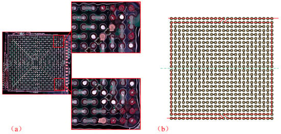
Figure 10.
The temperature cycling tests results in D101: (a) dye and pry test results, (b) typical solder joint failure locations.
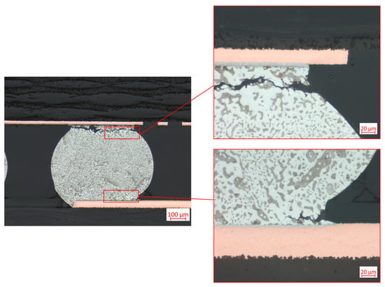
Figure 11.
A SEM of failed solder joint for the temperature cycling tests in D101.
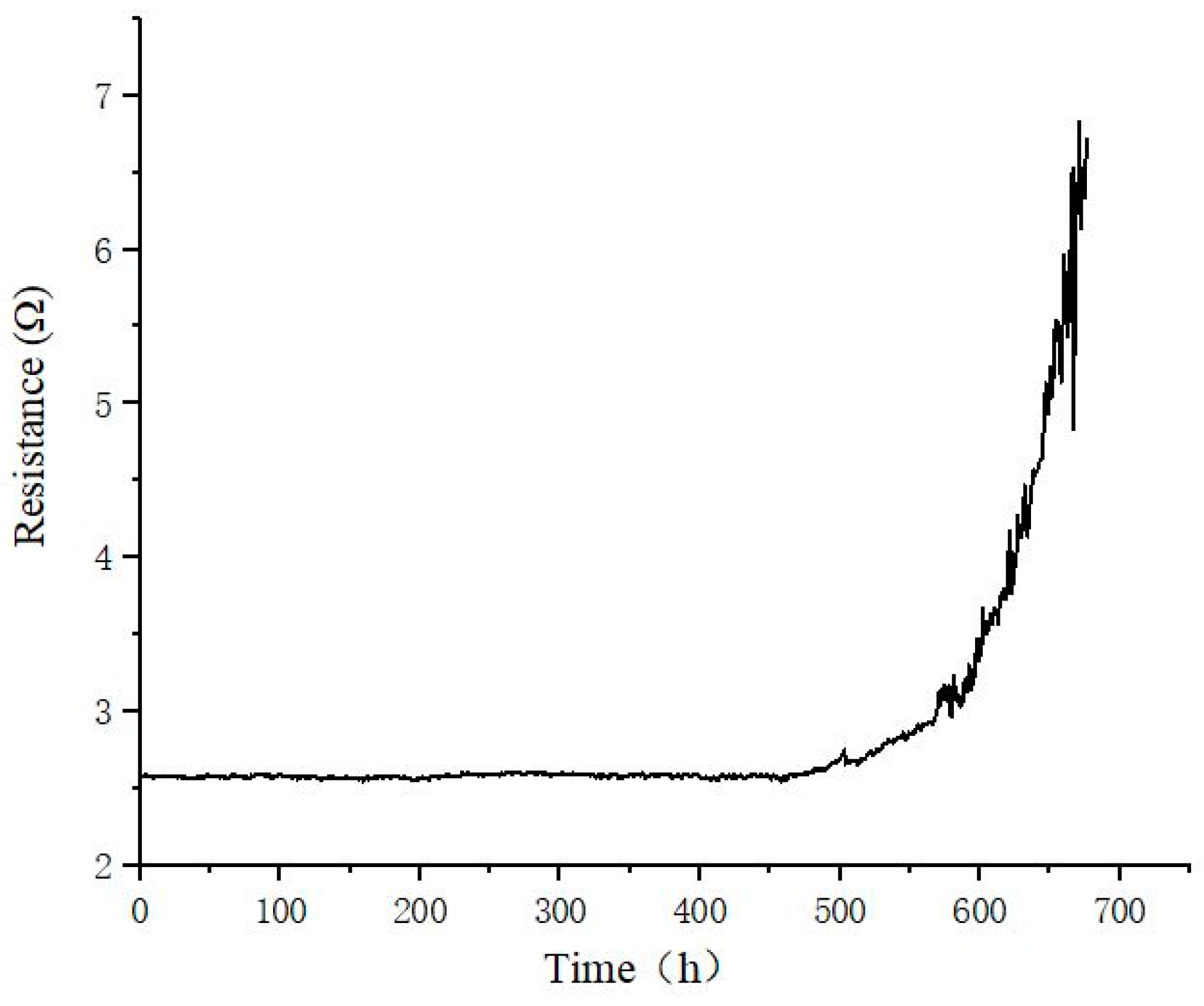
The lifetime distribution of the temperature cycling was listed in Table 7. The average lifetime of the 16 specimens was 525.5 h with a standard deviation of 40.4. There were almost no specimens with early failure, and the failure time was relatively concentrated. The fatigue life for temperature cycling was 589 h based on the test results. Experimental results accorded well with the simulation results. All specimens failed due to the increase in daisy chain resistance, and there was no open circuit phenomenon for the temperature cycling test. The resistance of the daisy chain circuit of specimen 16A as the function of time for the temperature cycling tests was shown in Figure 12. It could be seen that the resistance of the daisy chain increased gradually with time. The thermal fatigue crack propagation behavior caused the value of resistance to increase apparently with time.

Table 7.
Test results for temperature cycling.
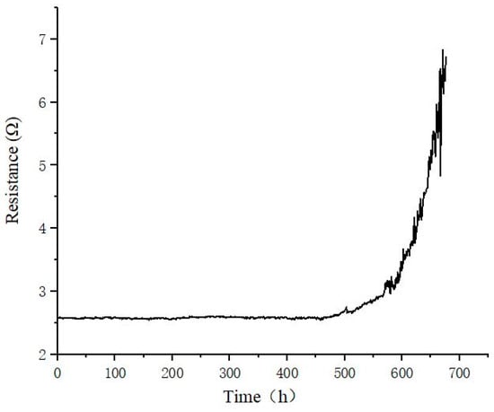
Figure 12.
The resistance of daisy chain circuit specimen 16A as the function of time for the temperature cycling tests.
3.2. Random Vibration Test Analysis
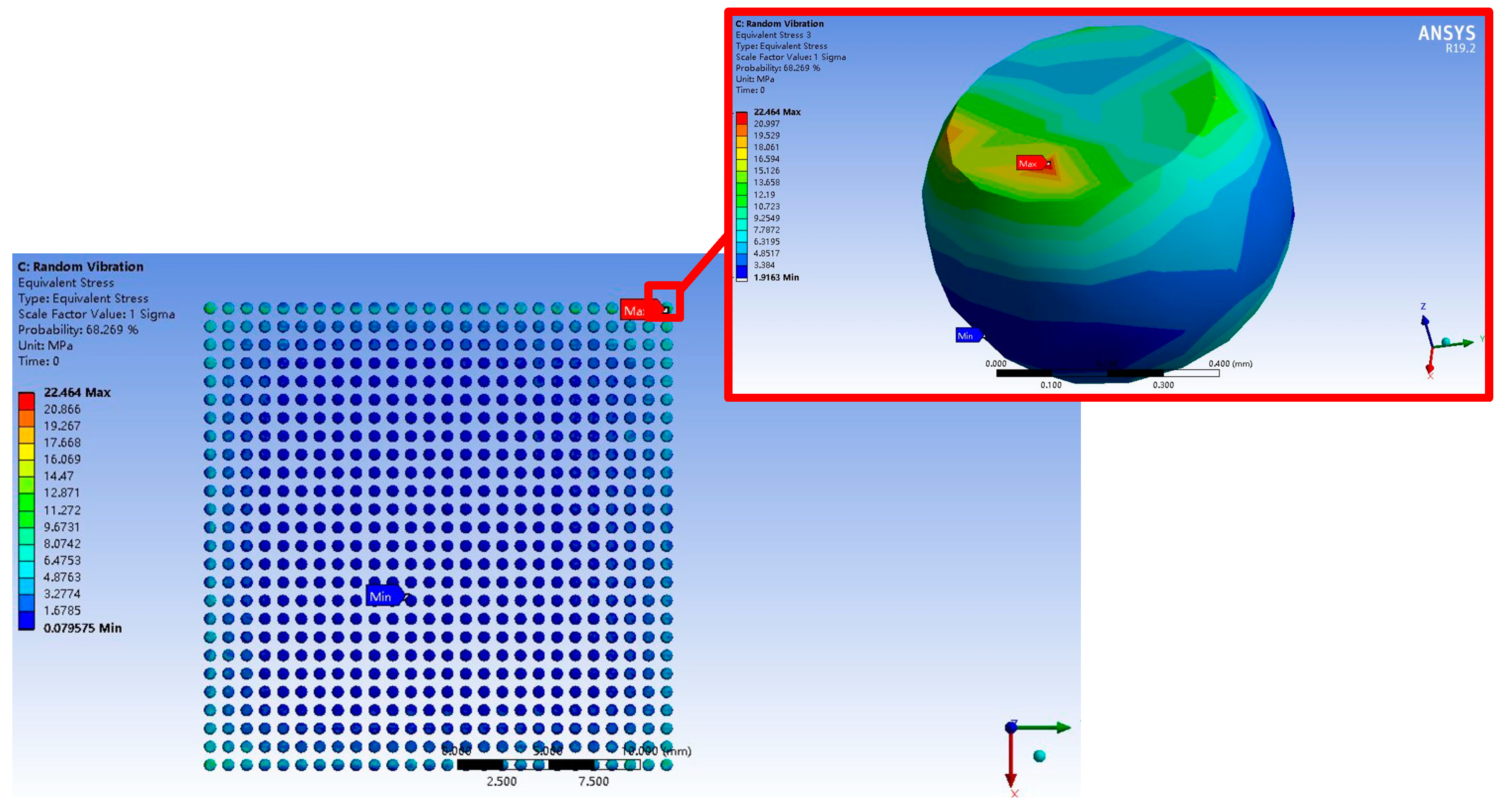
Using modal analysis, the natural frequencies of orders 1–6 were obtained, as shown in Table 8. Based on Steinberg’s three-band theory, the node displacement under random vibration is subject to a Gaussian distribution. Within the ±1σ, ±2σ and ±3σ distribution interval, the probability of instantaneous acceleration was 68.3%, 95.4% and 99.7%, respectively. The distribution of equivalent stress of 1σ in D101 was shown in Figure 13. The maximum stress was 22.464 MPa at the corner and the probability of occurrence was 68.3% under the random vibration.

Table 8.
The natural frequencies of order 1–6 of the specimen.
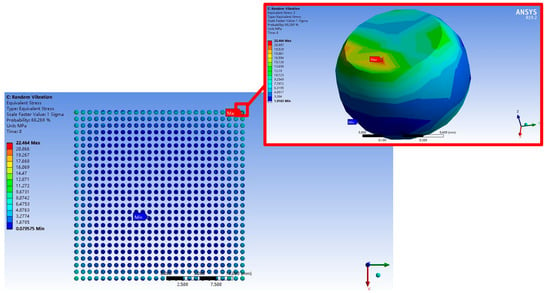
Figure 13.
The distribution of equivalent stress of 1σ in D101.
Manson’s empirical high cycle fatigue formula was used for life prediction as the following equation [23]:
where Δεt is the strain difference, E is the Elastic modulus, σu is the tensile strength, and Nf is the fatigue life time of the random vibration. Furthermore, the random vibration fatigue life should be calculated using Miner’s linear fatigue damage criterion and Steinberg’s model. The following equation can be used to calculate total fatigue damage:
where niσ is the actual number of cycles under −iσ~ + iσ strain amplitudes. Niσ is the number of cycles corresponding to iσ strain amplitudes. It is generally believed that when D = 1, the damage occurred.
The node displacement under random vibration is subject to Gaussian distribution; according to Steinberg’s three-band theory, n1σ, n2σ and n3σ could be given as the following equation:
N0+ stands for the number of positive zero crossings, which is dependent on the structure’s natural frequency and can be calculated as follows:
where Pi is power density spectrums at i-order nature frequency, fi is the i-order natural frequency of the structure, Ωi is the i-order angular frequency, and Qi = fi0.5 is the transmission rate at i-order nature frequency. Table 9 listed the mechanical response of the dangerous node under random vibration. The vibration fatigue life was calculated to be 11.75 h based on the equation above.

Table 9.
The mechanical response of the dangerous node under the random vibration.
Similarly, the failed component was mainly the larger BGA device D101. As shown in Figure 14, the dye and pry test results and typical locations of the failed solder joints were summarized for D101. The simulation results were well supported by the concentration of the failed solder joints in the upper right corner. The location of the break on the component side was shown in Figure 15. The failed solder joints’ cracks appeared as depicted in Figure 13 because of the calculated maximum equivalent stress concentrated along the interface between the copper pad and the risky solder connection.
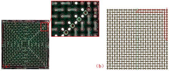
Figure 14.
The random vibration tests results in D101: (a) dye and pry test results, (b) typical solder joint failure locations.
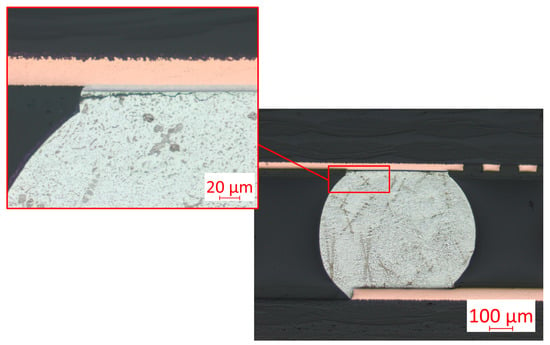
Figure 15.
A SEM of failed solder joint for the random vibration tests in D101.
The lifetime distribution of the random vibration was listed in Table 10. The average lifetime of the 16 specimens was 6.52 h with a standard deviation of 4.08. Compared with the temperature cycling test, the failure time was much shorter. The fatigue life for random vibration was 13.36 h based on the 16th failure specimen 29B results. The experimental result was slightly longer than the simulation results with an error of 12%. The failure of specimens was mostly due to the increase in daisy chain resistance, and there were two failures caused by an open circuit. The resistance of the daisy chain circuit of specimen 29B as the function of time for the random vibration tests was shown in Figure 16. The variety of resistance of the daisy chain was totally different compared with the temperature cycling test results. Before the failure, the resistance of the daisy chain fluctuated between a narrow range and rapidly increased when the failure occurred. The rapid crack propagation behavior caused the resistance value to increase significantly in a short time.

Table 10.
Test results for random vibration.
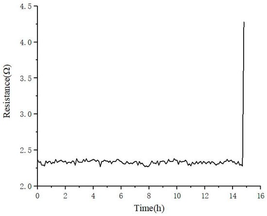
Figure 16.
The resistance of daisy chain circuit specimen 29B as the function of time for the random vibration tests.
3.3. The Combined Temperature Cycling and Random Vibration Analysis
The rapid life-prediction approach method might be used to calculate the combined temperature cycling and random vibration fatigue life [24]. By combining the damage caused by random vibration and the damage caused by a temperature cycle, the total damage normalized to a temperature cycle was calculated:
where D is the total accumulating damage, ni is the number of cycles, Ni is the vibration fatigue life of material under that stress level, and Th,Tl and Tav are the highest temperature, lowest temperature and average temperature in the temperature cycling test, respectively. th, tl and tav are the ratio of the corresponding temperature time to the total cycle time. Table 11 gave the mechanical response of the dangerous node. The combined test displayed greater sensitivity to the damage than the single random vibration test. The fatigue life was calculated to be 3.024 h based on Equation 7.

Table 11.
The mechanical response of the dangerous node under the combined temperature cycling and random vibration.
Figure 17 showed the typical failure locations of D101 subjected to the combined temperature cycling and random vibration loading conditions. Most of the cracks at failed solder joints were located on the component side, similar to the failure locations of single-temperature cycling and random vibration test. However, there was a great difference between the combined and single tests. On the one hand, not only D101 failed during the test, but also the QFP device D501 failed as well. As shown in Figure 18, the solder joints were more vulnerable on the component side and the pins fractured at the welding regions during the tests. On the other hand, all the specimens failed due to the open circuit rather than the increased daisy chain resistance.
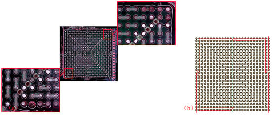
Figure 17.
The combined temperature cycling and random vibration tests results in D101: (a) dye and pry test results; (b) typical solder joint failure locations.

Figure 18.
A SEM of failed component of the combined temperature cycling and random vibration tests: (a) a solder joint in D101; (b) a pin in D501.
The lifetime distribution of the combined test was listed in Table 12. The average lifetime of the 16 specimens was 2.75 h with a standard deviation of 0.50. It was obvious that the combined fatigue life was even shorter than temperature cycling and random vibration test, which was reduced to 3.36 h. It could be indicated that the fatigue life calculated by the rapid life-prediction approach was acceptable considering the error. Moreover, as the temperature varied, the solder’s yield changed, indicating that the deformation was more significant during the vibration, leading to lower stress levels and fatigue life in the solder joints.

Table 12.
Test results for combined temperature cycling and random vibration.
4. Conclusions
In this study, 3D FE analyses and experiments were performed to evaluate the influence of the reliability of complex components under temperature cycling, random vibration and combined loading for airborne applications. The following conclusions are drawn:
- (1)
- For the temperature cycling test, the failed solder joints appeared on the corners, indicating that the experimental results accorded well with the simulation results. Thermal mismatch induced by the interconnection structure greatly affected the growth of cracks of bulk solder joints, especially on the component side. All specimens failed due to the increase in daisy chain resistance with a fatigue life above 500 h;
- (2)
- The fatigue life for the random vibration test was 13.36 h which was much shorter than the temperature cycling test of 589 h. A few open circuit phenomena could be observed above the test specimens. Miner’s linear fatigue damage criterion and Steinberg’s model could be fully used to predict an accurate fatigue life compared with the experimental result. The cracks were located on the component side, and the daisy chain resistance fluctuated between a narrow range and rapidly increased when the failure occurred;
- (3)
- The rapid life-prediction approach was able to accurately forecast the fatigue life with a minimal error when compared to the experimental result for the combined temperature cycling and random vibration test. The dependability design of the structure under coupled temperature cycling and random vibration loads may benefit from this technique;
- (4)
- All of the specimens failed owing to an open circuit once the QFP device failures were identified. Results showed that during the combined temperature cycling and random vibration testing, the solder junctions on the component side were more brittle and the pins shattered at the welding regions. Lowered stress levels and fatigue life in the solder joints were a result of the degradation of the yield strength of the solder brought on by temperature change. The designer should consider strengthening the protective measures at dangerous locations to improve reliability.
Author Contributions
Conceptualization, W.T.; writing—original draft preparation, H.C.; data curation, H.X.; writing—review and editing, H.W.; software, J.H. and C.P.; writing—review and editing, Z.C. All authors have read and agreed to the published version of the manuscript.
Funding
This research was funded by the National Natural Science Foundation of China, grant number 62104181.
Institutional Review Board Statement
Not applicable.
Informed Consent Statement
Not applicable.
Data Availability Statement
Not applicable.
Conflicts of Interest
The authors declare no conflict of interest.
Appendix A
Nomenclatures
| ρ (g/cm3) | Density |
| E (GPa) | Young’s modulus |
| v | Poisson’s ratio |
| α (1 × 10⁻⁶/K) | Coefficient of thermal expansion |
| s0 (MPa) | Initial value of deformation resistance |
| Q/R (1/K) | Activation energy |
| A (1/s) | Pre-exponential factor |
| ξ | Stress multiplier |
| m | Strain rate sensitivity of stress |
| h0 (MPa) | Hardening coefficient |
| ŝ (MPa) | Coefficient for deformation resistance saturation value |
| n | Strain rate sensitivity of saturation value |
| α | Strain rate sensitivity of hardening coefficient |
| Nf (h) | Fatigue lifetime |
| Δγp | Equivalent plastic strain |
| εf | Fatigue toughness coefficient |
| c | Fatigue toughness index |
| Δεt | Strain difference |
| σu | Tensile strength |
| niσ | Number of cycles under −iσ~ + iσ strain amplitudes. |
| Niσ | Number of cycles corresponding to iσ strain amplitudes |
| Pi (g2/Hz) | Power density spectrums |
| fi | i-order natural frequency |
| Ωi | i-order angular frequency |
| D | Total accumulating damage |
| ni | Cycles number |
| Ni (h) | Vibration fatigue life |
| Th (°C) | Highest temperature |
| Tl (°C) | Lowest temperature |
| Tav (°C) | Average temperature |
| th | Ratio of the highest temperature time to the total cycle time |
| tl | Ratio of the lowest temperature time to the total cycle time |
| tav | Ratio of the average temperature time to the total cycle time |
References
- Qi, H.; Osterman, M.; Pecht, M. A Rapid Life-Prediction Approach for PBGA Solder Joints Under Combined Thermal Cycling and Vibration Loading Conditions. IEEE Trans. Compon. Packag. Technol. 2009, 32, 283–292. [Google Scholar] [CrossRef]
- Arabi, F.; Gracia, A.; Delétage, J.Y.; Frémont, H. Sequential combined thermal cycling and vibration test and simulation of printed circuit board. Microelectron. Reliab. 2018, 88–90, 768–773. [Google Scholar] [CrossRef]
- Tian, W.; Cui, H.; Yu, W. Analysis and Experimental Test of Electrical Characteristics on Bonding Wire. Electronics 2019, 8, 365. [Google Scholar] [CrossRef]
- Jaafar, N.B.; Ching, E.W.L. Study on ultra low loop copper wire bonding process using 0.8 mils Cu wire for low profile package applications. In Proceedings of the 2015 IEEE 17th Electronics Packaging and Technology Conference (EPTC), Singapore, 2–4 December 2015; pp. 1–4. [Google Scholar]
- Cui, H.; Tian, W.; Zhao, X.; Chen, S.; Chen, Z. Effect of the reflow process on IMC growth for different devices and complex components. Smart Mater. Struct. 2022, 31, 115028. [Google Scholar] [CrossRef]
- Yuan, C.; Fan, X.; Zhang, G. Solder Joint Reliability Risk Estimation by AI-Assisted Simulation Framework with Genetic Algorithm to Optimize the Initial Parameters for AI Models. Materials 2021, 14, 4835. [Google Scholar] [CrossRef]
- Vieira, D.N.; Lima, A.; Santos, D.; Rodrigues, N.; Carvalho, V.; Puga, H.; Teixeira, S.F.C.F.; Teixeira, J.C. Prediction of Solder Joint Reliability with Applied Acrylic Conformal Coating. J. Electron. Mater. 2022, 51, 273–283. [Google Scholar] [CrossRef]
- Jayesh, S.; Elias, J. Experimental and finite element analysis on determining the fatigue life of pb-free solder joint (Sn-0.5Cu-3Bi-1Ag) used in electronic packages under harmonic loads. Int. J. Model. Simul. Sci. Comput. 2020, 11, 2050020. [Google Scholar] [CrossRef]
- Amalu, E.H.; Ekere, N.N. Damage of lead-free solder joints in flip chip assemblies subjected to high-temperature thermal cycling. Comput. Mater. Sci. 2012, 65, 470–484. [Google Scholar] [CrossRef]
- Kanai, H.; Kariya, Y.; Sugimoto, H.; Abe, Y.; Yokoyama, Y.; Ochi, K.; Hanada, R.; Soda, S. Fatigue Life Prediction of Die-Attach Joint in Power Semiconductors Subjected to Biaxial Stress by High-Speed Thermal Cycling. Mater. Trans. 2022, 63, 759–765. [Google Scholar] [CrossRef]
- Liu, D.S.; Chen, Y.W.; Tsai, C.Y. Thermal Stress Analysis of Chip Scale Packaging by Using Novel Multiscale Interface Element Method. Math. Probl. Eng. 2018, 2018, 4962498. [Google Scholar] [CrossRef]
- Pan, J.; Chou, T.; Bath, J.; Willie, D.; Toleno, B.J.J.S.; Technology, S.M. Effects of reflow profile and thermal conditioning on intermetallic compound thickness for SnAgCu soldered joints. Solder. Surf. Mt. Technol. 2009, 21, 32–37. [Google Scholar] [CrossRef]
- Kang, M.-S.; Jeon, Y.-J.; Kim, D.-S.; Shin, Y.-E. Degradation characteristics and Ni3Sn4 IMC growth by a thermal shock test in SAC305 solder joints of MLCCs applied in automotive electronics. Int. J. Precis. Eng. Manuf. 2016, 17, 445–452. [Google Scholar] [CrossRef]
- Dalton, E.; Ren, G.; Punch, J.; Collins, M.N. Accelerated temperature cycling induced strain and failure behaviour for BGA assemblies of third generation high Ag content Pb-free solder alloys. Mater. Des. 2018, 154, 184–191. [Google Scholar] [CrossRef]
- Wentlent, L.; Alghoul, T.M.; Greene, C.M.; Borgesen, P. Effects of Amplitude Variations on Deformation and Damage Evolution in SnAgCu Solder in Isothermal Cycling. J. Electron. Mater. 2018, 47, 2752–2760. [Google Scholar] [CrossRef]
- Xia, J.; Li, G.; Li, B.; Cheng, L.; Zhou, B. Fatigue life prediction of Package-on-Package stacking assembly under random vibration loading. Microelectron. Reliab. 2017, 71, 111–118. [Google Scholar] [CrossRef]
- Baishya, K.; Harvey, D.M.; Partida Manzanera, T.; Zhang, G.; Braden, D.R. Failure patterns of solder joints identified through lifetime vibration tests. Nondestruct. Test. Eval. 2022, 38, 147–171. [Google Scholar] [CrossRef]
- Xia, J.; Cheng, L.; Li, G.; Li, B. Reliability study of package-on-package stacking assembly under vibration loading. Microelectron. Reliab. 2017, 78, 285–293. [Google Scholar] [CrossRef]
- Kim, Y.K.; Hwang, D.S. PBGA packaging reliability assessments under random vibrations for space applications. Microelectron. Reliab. 2015, 55, 172–179. [Google Scholar] [CrossRef]
- Ding, Y.; Tian, R.; Wang, X.; Hang, C.; Yu, F.; Zhou, L.; Meng, X.; Tian, Y. Coupling effects of mechanical vibrations and thermal cycling on reliability of CCGA solder joints. Microelectron. Reliab. 2015, 55, 2396–2402. [Google Scholar] [CrossRef]
- Ghaderi, D. Reliability analysis for TO-247 multilayered power module packaging under mechanical oscillation based on finite element method. Microelectron. Reliab. 2021, 118, 114046. [Google Scholar] [CrossRef]
- Engelmaier, W. Fatigue Life of Leadless Chip Carrier Solder Joints During Power Cycling. IEEE Trans. Compon. Hybrids Manuf. Technol. 1983, 6, 232–237. [Google Scholar] [CrossRef]
- Yang, P.; Tang, X.; Liu, Y.; Wang, S.; Yang, J. Dynamic reliability approach of chip scale package assembly under vibration environment. Microelectron. Int. 2014, 31, 71–77. [Google Scholar] [CrossRef]
- Qi, H.; Osterman, M.; Pecht, M. Plastic Ball Grid Array Solder Joint Reliability for Avionics Applications. IEEE Trans. Compon. Packag. Technol. 2007, 30, 242–247. [Google Scholar] [CrossRef]
Disclaimer/Publisher’s Note: The statements, opinions and data contained in all publications are solely those of the individual author(s) and contributor(s) and not of MDPI and/or the editor(s). MDPI and/or the editor(s) disclaim responsibility for any injury to people or property resulting from any ideas, methods, instructions or products referred to in the content. |
© 2023 by the authors. Licensee MDPI, Basel, Switzerland. This article is an open access article distributed under the terms and conditions of the Creative Commons Attribution (CC BY) license (https://creativecommons.org/licenses/by/4.0/).

