Article

Development of Luminescent Nd-Doped LaNbO Compound Thin Film Growth by Magnetron Sputtering for the Improvement of Solar Cells

by
Eduardo Salas-Colera
1,*,
Miguel Tardío
1,
Elisa García-Tabarés
1,
Belén Perea
1,
Miguel L. Crespillo
2,
Juan Enrique Muñoz-Santiuste
1 and
Beatriz Galiana
1
1
Departamento de Física, Universidad Carlos III de Madrid, Avda. Universidad 30, 28911 Leganés, Madrid, Spain
2
Centro de Microánalisis de Materiales, CMAM-UAM, C) Faraday 3, 28049 Cantoblanco, Madrid, Spain
*
Author to whom correspondence should be addressed.
Crystals 2023, 13(2), 159; https://doi.org/10.3390/cryst13020159
Submission received: 15 December 2022 / Revised: 11 January 2023 / Accepted: 12 January 2023 / Published: 17 January 2023
(This article belongs to the Special Issue Research and Applications of Metal Oxide Thin Films)

Abstract

:
Nd3+-doped LaNbO phosphor thin films were prepared by radio-frequency magnetron sputtering on Si substrates. The effects of a 1% Nd-doping concentration, after annealing at 1200 °C for 12 h, on the light-emitting properties of the sputtered thin films were characterized via several experimental techniques and deeply discussed. Photoluminescence characterization showed strong emission peaks typical of Nd3+ centers at 880 nm and 1060 nm when a 325 nm wavelength laser source was applied. Similar responses were detected in Nd3+-doped La3NbO7 powder samples fabricated by the solid-state reaction method. The coexistence of two phases (LaNbO4 and La3NbO7) in the thin films with higher nominal thickness was clearly identified based on different structural analyses. The promising results open the possibility for developing phosphor substrates as a preliminary step for the improvement of solar cells based on photon recycling mechanisms.

1. Introduction

Nowadays, Si-based solar cells have reached a world record efficiency of 26.3%, corresponding to 91% of their theoretical limit [1], while GaAs monojunction solar cells have also seen saturated efficiency improvement in the last decade [2]. However, multijunction solar cells have to deal with the limitation of current matching, in which the subcell with the lowest photocurrent determines the current of the whole device. Consequently, research on device architecture improvement is a hot topic to improve the efficiency of solar cell devices.
In this work, we focus on the use of rare-earth-doped oxides as a novel approach to tune the resulting spectrum that a solar cell will transform into a photocurrent [3,4]. The proposal is mainly based on the photon recycling mechanisms [5] presented by phosphor materials. They can be up-conversion (UC), which consists of the addition of two low-infrared (IR) photons to emit a visible energy (Vis) photon, or down-conversion (DC) [6] when a high-energy (UV) photon splits into two lower-energy (Vis) photons. In both cases, the aim is to recycle the photons in a dual way: photons with lower energy than the bandgap of the solar cell are not absorbed, and those with high energy generate thermalization losses.
Rare-earth-based, up/down-converting phosphor films produced by sputtering represent the new, sophisticated generation in materials science and engineering for labeling technologies, sensors, optical data storage, telecommunications or solar cells [7]. These light-emissive materials consist of a host matrix in combination with a transition metal or rare earth ions as activators, such that the host matrix allows minimizing non-radiative transition processes between the rare earth ions and the matrix itself. There are different phosphor systems to be used in solar cells [7,8], such as fluorides [9], vanadates [10] or yttriates [11]. Among phosphor materials, lanthanum niobate compounds have recently attracted interest due to a combination of dielectric and catalytic properties in combination with high chemical stability for use in energy storage [12].
In addition, rare-earth-doped lanthanum niobates have emerged as a very motivating material due to their interesting luminescence properties for solar cell-based applications. On one hand, Er3+-doped La3NbO7 powder samples show a strong green emission band centered at 550 nm [13]. On the other, Yb3+/Tb3+-doped LaNbO4 powder samples also show a strong signal from Tb ions mainly centered at 477 and 543 nm [14].
The crystal structure strongly determines the optical properties of lanthanum niobate-based phosphor materials [15,16]. The crystal structure is determined by the synthesis method used [17]. There is a large number of deposition methods to synthesize rare-earth-doped phosphor oxides, such as the conventional solid-state reaction [13,18], sol-gel route [19], spin coating [20] or sputtering [21]. The structural properties of several lanthanide niobates have already been studied in powder samples [22].
Current efforts to improve the quantum efficiency of UC and DC processes are focused on the selection of a suitable host for this activator ion. Among the lanthanum niobates, the weberite-type La3NbO7 compound shows an orthorhombic crystal structure and Cmcm space group [23], and is well studied as its relatively low phonon frequencies inhibit nonradiative pathways, thus allowing the rare earth ions’ electrical levels to have large lifetimes (low phonon energy is required to reduce the multiphonon relaxation rate) [24,25,26]. This material has attracted great attention because it exhibits interesting properties, such as photocatalytic [27] or magnetic [28] properties, or as a possible electrolyte for solid-state fuel cells [29] due to its chemical stability [30].
Sputtering magnetron is one of the most widely used deposition techniques for the growth of thin films and coatings [31]. This technique allows for modifying and controlling the structural properties of a deposited material by varying the growth parameters [17]. Sputtering magnetron has already been used to deposit LaNbO4 thin films [32], but there has been no work reported on the growth of La3NbO7 weberite-type structures in thin film form by sputtering magnetron.
We propose the deposition of rare-earth-doped oxides by means of magnetron sputtering on conventional Si substrates to develop a process compatible with solar cell fabrication. In particular, Nd3+-doped weberite-type La3NbO7 was chosen due to its promising properties, high chemical stability and relatively flexible structure that can accommodate large cations [33]. Nd3+ ions easily incorporate into the weberite lattice, substituting La ions because of their similar ionic radii. In fact, full La–Nd substitution has been achieved and the Nd3NbO7 compound has been fully characterized from a crystallographic point of view [34], whereas high disorder occurs in compounds with rare earth ions with ionic radii smaller than that of Tb [35].
Consequently, the main aim of this work is to reproduce the previous luminescence properties achieved in powder samples (grown by the solid-state reaction) in thin film samples grown by magnetron sputtering. The success of this work would allow the development of phosphor thin films based on lanthanum niobates doped with rare earth metals to be used as substrates in the fabrication of solar cells to improve their efficiency.

2. Materials and Methods

The starting oxide studied was nominal La3NbO7 doped with Nd3+ (1%). The sputtering target, with a thickness of 3.2 mm and diameter of 50.8 mm, was developed by mixing stoichiometric amounts of the high-purity powdered oxides La2O3 (99.9%), Nb2O5 (99.9%) and Nd2O3 (99.99%) from Alfa Aesar. Then, the mixture was pressed into a circular pellet with appropriate dimensions using a hydraulic press and sintered in air at 1200 °C for 12 h [36]. Energy-Dispersive X-ray Spectroscopy (EDX) measurement performed via scanning electron microscopy (SEM) confirmed the expected stoichiometry of the home-made sputtering target. The 1% Nd-doped La3NbO7 phosphor thin film samples were grown on p-type double-sided polished Si (100) wafers from Silicon Materials (Karl Lichtensterm). Finally, the substrates were cleaned in a consecutive ultrasonic bath of acetone (99.7%) and ethanol (99.7%) for 20 min at a temperature of 50 °C and then dried under an airflow.
The deposition chamber was initially pumped to a base vacuum pressure lower than 5.3 · 10−6 mbar. Then, high-purity Ar (99.999%) was introduced to the chamber to clean the substrates for 15 min at a pressure of 5.3 · 10−6 mbar prior to the deposition of Nd-doped La3NbO7 thin films. Finally, the pressure in the chamber was increased to the deposition working pressure of 5.0 · 10−3 mbar of Ar gas. Nd-doped La3NbO7 thin films were then deposited at room temperature under an Ar gas flow of 25 sccm to keep the working pressure of 5.0 · 10−3 mbar constant. The distance between the substrate and target was maintained at 100 mm. The deposition times and radiofrequency (RF) powers were varied. The sputtering condition values for each sample under study are presented in Table 1.
Afterward, all of the samples were annealed at 1200 °C for 12 h in air to complete the overall La3NbO7 synthesis reaction (Equation (1)) [34].
3La2O3 + Nb2O5 → 2La3NbO7,
The overall La3NbO7 synthesis reaction included two different phases (Equations (2) and (3) respectively):
La2O3 + Nb2O5 → 2LaNbO4,
2La2O3 + 2LaNbO4 → 2La3NbO7,
The structural properties were characterized by High-Resolution X-ray Diffraction (HR-XRD), Rutherford Backscattering Spectroscopy (RBS), Scanning Electron Microscopy (SEM) and Transmission Electron Microscopy (TEM). The chemical composition was measured by Energy Dispersive X-ray Spectroscopy (EDX) in the Scanning TEM mode (STEM).
HR-XRD analysis was carried out using a Philips X’Pert MPD diffractometer. Measurements were performed using a Cu–Kα radiation source at 40 keV and 40 mA in (θ/2θ) Bragg–Brentano geometry. The instrument was equipped with a curved graphite monochromator to increase the resolution and reduce the background noise. The patterns were measured in the 2θ range from 20° to 60°, with a 0.02° step scan and 3 s per step.
The RBS characterization process was carried out using the 5.0 MV linear tandem accelerator facility located at the Center for the Microanalysis of Materials (CMAM) [37] located at the Universidad Autónoma de Madrid (UAM) campus. The RBS analysis conducted in the standard (STD) beamline chamber was used to quantitatively determine the in-depth concentrations and in-depth profiles of La, Nb, O and Nd elements. The STD end station consisted of a custom-designed Ultra-High-Vacuum (UHV) target chamber with several ports located at three horizontal levels for vacuum control and analytical capabilities. A collimated 2.0 MeV H+ beam extracted from the accelerator (divergence of ~0.1°) with a particle flux of 5.0 · 1012 cm−2s−1 and a probe size of 1.5 × 1.5 mm2 was used. A Si barrier particle detector (ORTEC, New York, NY, USA) placed in IBM geometry [38] with respect to the sample, fixed at a scattering angle of 170° relative to the incoming beam, with a solid angle of (4.1 ± 0.1)·10−3 sr and energy resolution of 12 keV was used to collect the signal of the backscattered H+ yield from the samples. The manipulator with a 3-angular axis goniometer from Panmure Instruments with an angular resolution better than ±0.01° and ±0.1 mm for vertical movement enabled the probe beam to be positioned on the selected sample. Precise computer-controlled manipulator movements were performed using home-made acquisition software. The RBS spectra were fitted by SIMNRA software version 7.02 [39] with calculations using the resonant cross section provided by SigmaCalc version 2.0.
SEM characterization was carried out using an FE-SEM TENEO LoVac microscope from the FEI company (Hillsboro, Oregon, OR, USA). TEM analysis was performed on thin cross-section samples prepared in a Focused Ion Beam (FIB) and examined in a Philips Tecnai F20 operated at 200 kV with a STEM module and High-Angle Annular Detector (HAAD) for Z-contrast imaging.
Finally, photoluminescence measurements in the visible range were carried out at room temperature using a Horiba Jovin-Ybon LabRAM HR800 system, where samples were excited by a 325 nm HeCd laser on an Olympus BX 41 confocal microscope. Photoluminescence measurements in the near-IR range (spectral range from 900 to 1800 nm) were performed with a Hamamatsu photonic multi-channel analyzer PMA-11. A 520 nm laser diode was used as the excitation source.

3. Results and Discussion

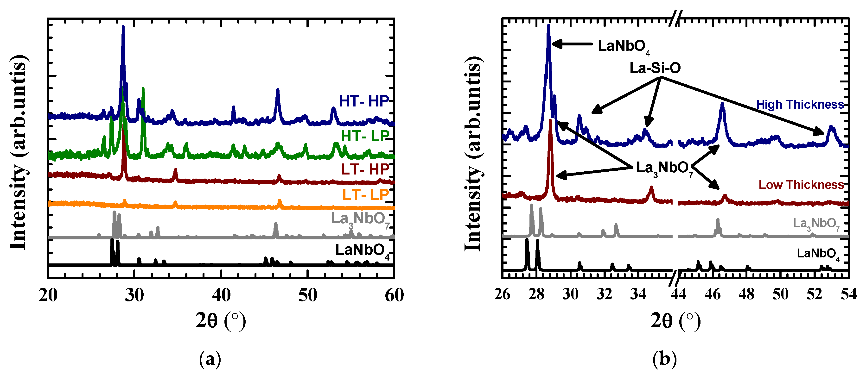
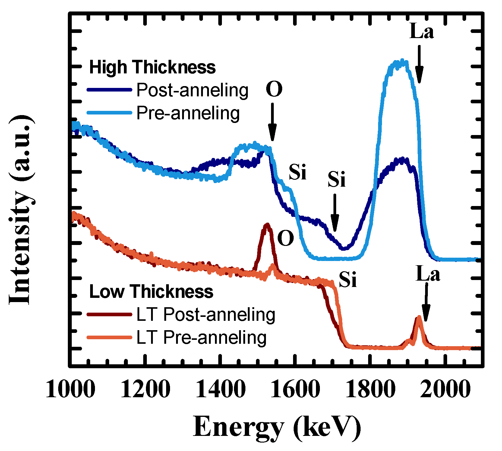
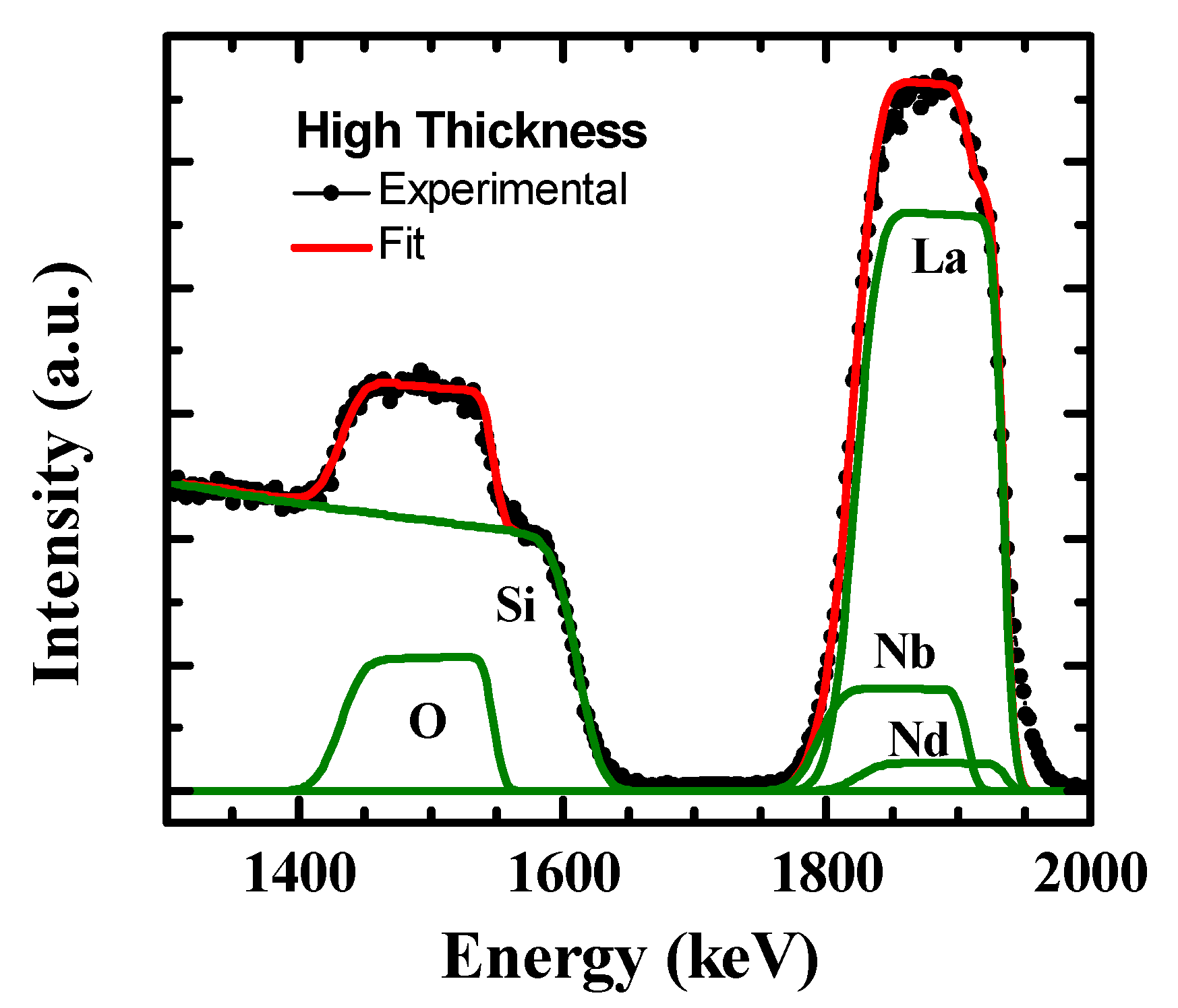
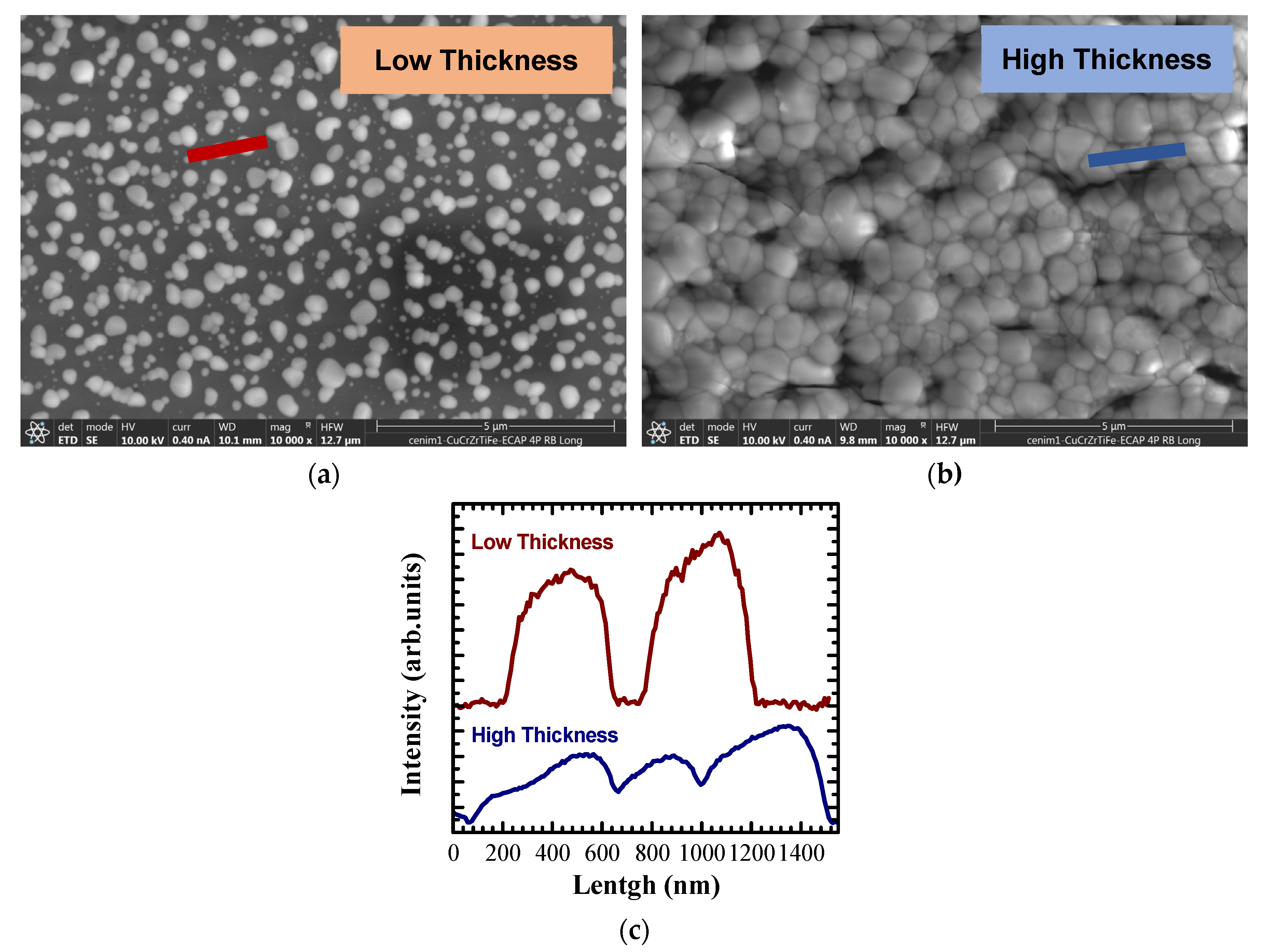
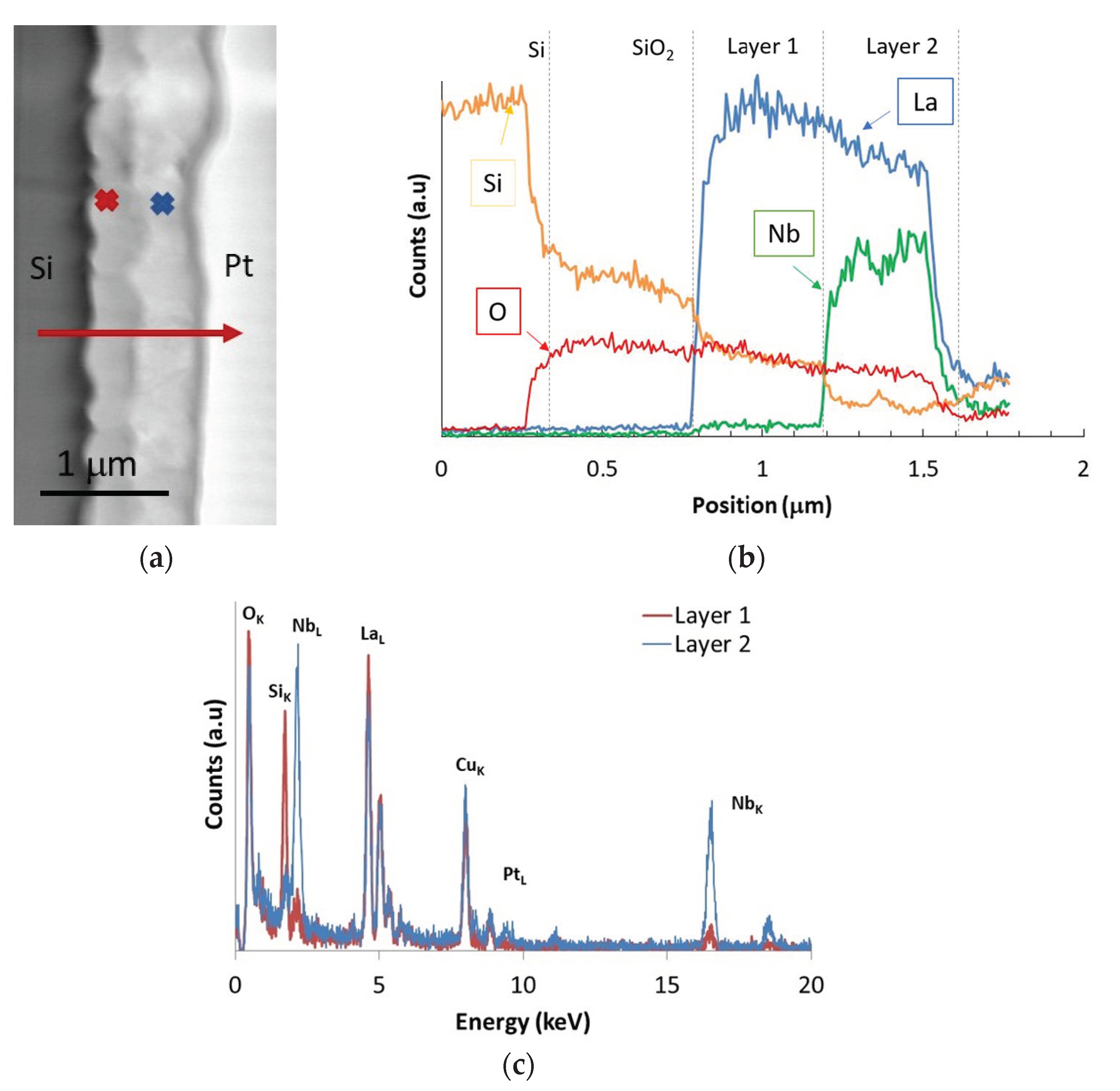
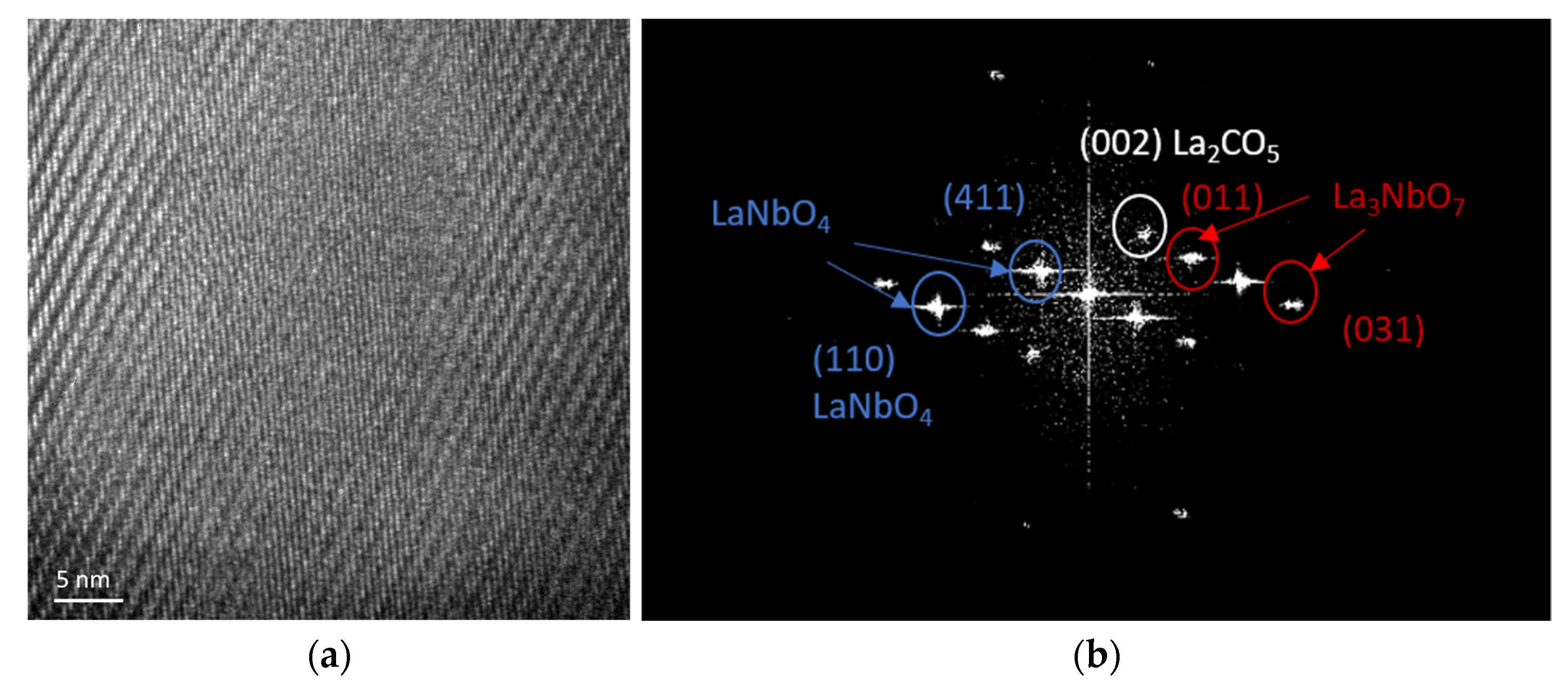
3.1. Structural Properties—“Composition and Structural Analysis: XRD, RBS, SEM and TEM Measurements”

The studied samples were deposited under different sputtering conditions, combining low/high RF powers and deposition times (see Table 1). HR-XRD characterization was carried out to study the crystal structure of Nd-doped lanthanum niobate thin films. Figure 1a compares the diffraction patterns of the samples under study with the simulated diffraction pattern from the two main structures of lanthanum niobates: orthorhombic space group Cmnm (nº63) for the weberite-like La3NbO7 structure and monoclinic C2/c (nº15) for the scheelite-type LaNbO4. Firstly, it can be observed that the RF power variation did not result in relevant differences in the crystallinity of the samples (HT-HP vs. HT-LP and LT-HP vs. LT-LP). Conversely, for the same RF power, the diffraction patterns of the HT samples showed a larger variety of diffraction peaks compared with the LT samples. Figure 1b shows the comparison between samples of two different thicknesses (i.e., HT and LT) with the simulated diffraction pattern from the two main structures of lanthanum niobates.
The patterns of both LT samples showed the expected main diffraction peaks of La3NbO7 compounds at 28.8° and 46.8°. The slight 2θ shift was associated with the substitution of the La3+ ion for Nd3+ (the cation site occupancy is a very important structural parameter that plays a key role in the luminescence efficiency). In both HT samples, the diffraction peak related to the LaNbO4 compound was also observed at 28.6°. In this case, the resulting experimental data could be consistent with the existence of both phases, as the interplanar distances of both compounds were close. In addition, the diffraction peaks associated with the formation of La-Si-O-based compounds and SiO2 were observed in thin films deposited for a long time. This fact could be related to the interaction between the silicon substrate and sputtered layer during the annealing process, which provoked the formation of secondary phases, such as LaSi (2θ = 30.9°). Moreover, the presence of La2O3 was observed (2θ = 30.5°). The presence of both La2O3 and LaNbO4 compounds meant that the second stage of the overall La3NbO7 synthesis reaction (see Equation (3)) was not totally completed, most likely due to the higher thickness.
Rutherford backscattering spectroscopy characterization was performed to study the structural properties of the thin film samples. Figure 2 shows the RBS spectra measured for the HT and LT samples before and after the annealing procedure. In the pre-annealed HT sample, a broad peak associated with the La, Nb and Nd signals was observed in the energy region between 1800 and 1950 keV, mostly associated with the La contribution. Meanwhile, for the pre-annealed LT sample, the La–Nd peak located at around 1925 keV and the Nb peak placed at around 1900 keV could be clearly identified. Regarding the post-annealing samples, two main features could be clearly observed. Firstly, experimental measurements revealed the formation of a much thicker SiO2 layer between the Nd-doped lanthanum niobate top layer and silicon substrate in both types of samples. This was deduced from the increase in the signal of the buried oxygen atoms, centered at 1550 keV for the surface signal, toward lower energy values (1500 keV for the case of the LT samples and 1325 keV for the HT samples), together with the shift to lower energies of the position associated with the silicon substrate. This could be clearly observed in the case of the LT samples, where the Si substrate peak changed from an energy of 1725 keV (pre-annealed) to 1675 keV (post-annealed); however, for the HT samples, the Si signal peak had two main contributions: experiencing an overall shift toward higher energies, from an energy of 1625 keV, corresponding to the Si substrate (pre-annealed), to 1725 keV, associated with the Si signal from the mixed (top) layer (post-annealed). The latter suggests some Si-induced out-diffusion reaching the Nd-doped lanthanum niobate (top) layer. On the other hand, some La segregation towards the SiO2 layer occurred during the annealing procedure, as observed clearly in the spectrum of the post-annealing HT thin film, where the La lower energy side at 1775 keV (pre-annealed) shifted to lower energies of 1725 keV (post-annealed). This result agrees with the previous HR-XRD characterization (Figure 1b), reinforcing the hypothesis of the formation of La-Si-O compounds and the presence of higher-Nb-concentration lanthanum niobate LaNbO4 compounds in combination with the expected weberite-type La3NbO7 in the HT samples.
An example of the compositional fitting of the HT thin film is plotted in Figure 3. By fitting, the expected La2.97Nd0.03NbO7 stoichiometry can be obtained for the full sample. On the contrary, in the post-annealing thin films, the element concentration could be determined, but the type of La-Si-O compounds formed in the mixed layer could not be defined.
High-resolution SEM and TEM microscopy techniques were used to characterize the morphology and composition of the sputtered thin film layer. Figure 4a,b show plan-view SEM images of LT and HT samples, respectively. In addition, Figure 4c presents the intensity profiles for several particles in each sample. It can be clearly observed that the LT sample presented a non-continuous layer. It was formed mainly by 100–400 nm-sized particles, although smaller-sized particles were also observed. On the contrary, the HT thin film sample was a continuous layer, formed by the coalescence of 200–600 nm-sized particles.
Figure 5 presents cross-section TEM images of the four different samples under study. As it can be observed, besides the sputtering RF power used, the LT samples were not continuous (Figure 5a,b), with variable island sizes ranging from 400 nm to 50 nm in the growth plane. On the other hand, the HT samples were continuous, with medium total thicknesses of 800 nm and 1040 nm for low and high RF power, respectively. Subsequently, the growth rates for the 50 W- and 80 W-sputtered samples were 3.8 nm/min and 4.5 nm/min, respectively. Analyzing these last samples in more detail, it can be observed that the layer was not homogenous, i.e., it was formed by two sublayers.
EDX measurements in the STEM mode were carried out to determine the composition of the sublayers observed in the HT samples. Figure 6a shows a Z-contrast STEM cross-section image of the HT-HP sample. The image clearly shows the existence of two different layers (marked with red and blue crosses). Figure 6b shows the compositional profiles of O, La and Nb elements for the HT thin film sample. The data were obtained by means of punctual spectra following the red arrow in the STEM image of Figure 6a. In addition, punctual EDX spectra (Figure 6c) with a higher dwell time were obtained for each sublayer for better chemical quantification. The EDX data analysis revealed and confirmed the formation of a SiO2 layer, most likely due to the ex situ post-annealing of the samples. Regarding the properties of the sputtering layers, it can be observed that La was detected throughout the whole structure, while Nb was concentrated in the upper layer of the sample (named layer 2 in Figure 6b). The quantitative EDX analysis from the punctual spectra of Figure 6c produced a La/Nb ratio close to 1 for layer 2. This suggests that the LaNbO4 phase was present together with the weberite-type La3NbO7. This coexistence of phases could be explained by the fact that Nd3+ ions disturbed the necessary secondary La2O3 + LaNbO4 → La3NbO7 reaction and eventually became responsible for the segregated phases, as has been reported when using Er3+ as a dopant [13].
To further investigate the crystallinity of the layers involved, Figure 7 shows a high-resolution image of the most external layer (named Layer 2 in Figure 6c) of the HT-HP sample. The Fast Fourier Transform (FFT) of the complete image, which simulates the experimental Electron Diffraction Pattern (EDP), can be seen in Figure 7b. According to the interplanar spacings determined from Figure 7b, the coexistence of at least two phases, LaNbO4 and La3NbO7, was observed, being coherent with the XRD results presented in Figure 1. We identified the following planes of La3NbO7: (011) with an interplanar distance d = 0.629 nm and (031) with d = 0.334 nm, forming an angle of 27°. For LaNbO4, we identified the planes (110) with d = 0.499 nm and (411) with d = 0.135 nm, forming an angle of 34°. Finally, we observed a spot for La2CO5, more concretely, (002) with d = 0.798 nm.

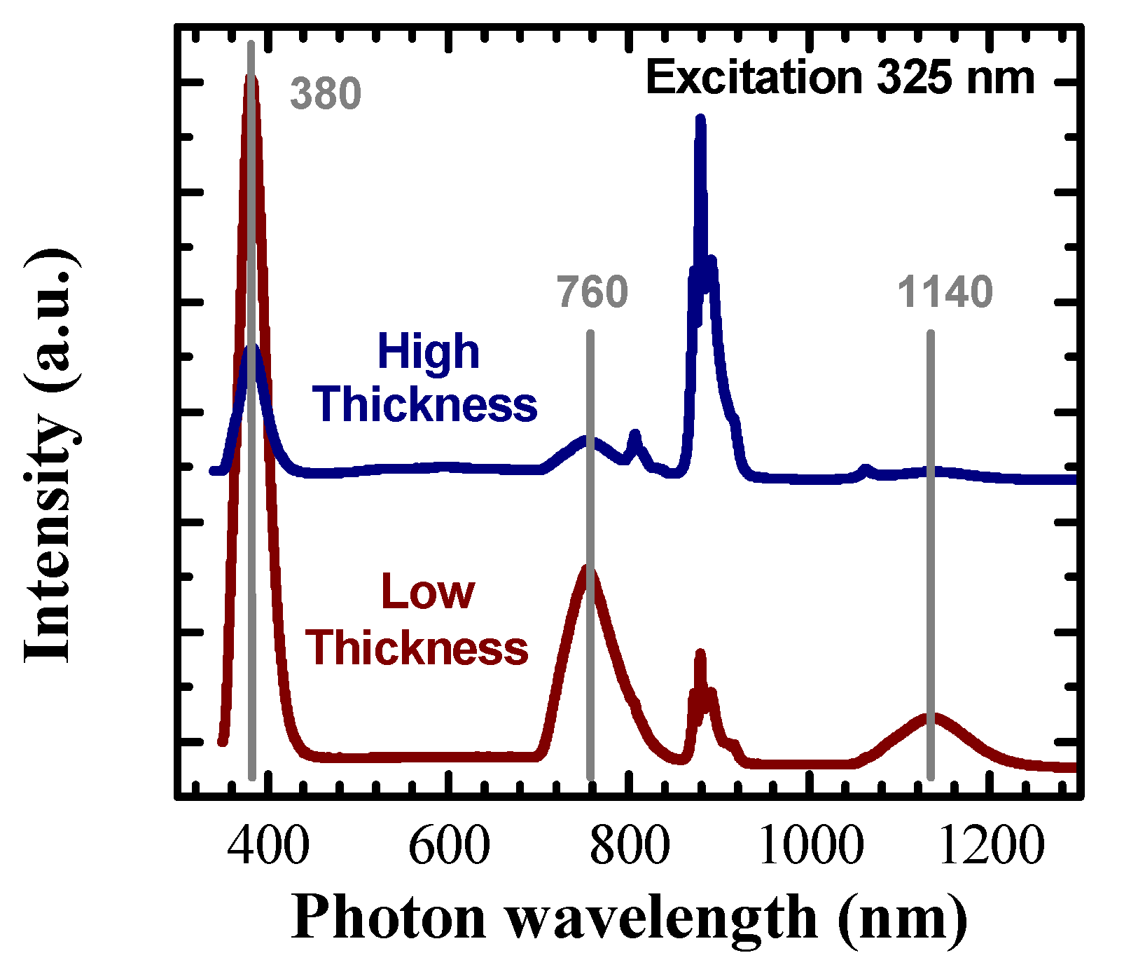
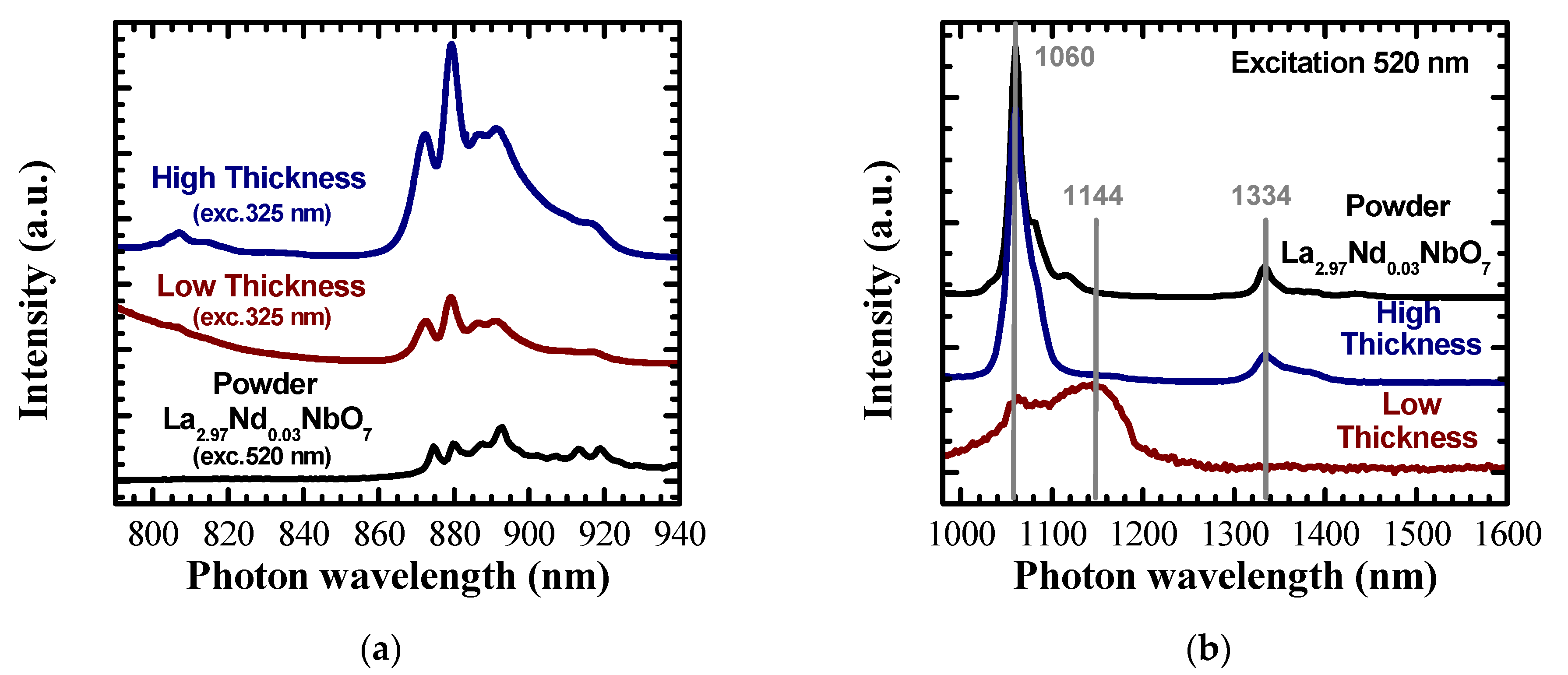
3.2. Luminescence Properties

The optical properties of the Nd3+-doped lanthanum niobate sputtered thin film samples were characterized by photoluminescence spectroscopy as a function of the sputtering growth conditions. This step was essential to achieve the main objective of this research, which was to produce an optically active rare-earth-doped oxide for use in solar cell devices to improve their efficiency.
Figure 8 shows the visible range of the photoluminescence spectra for the two different Nd-doped samples as functions of the layer thicknesses. The excitation wavelength was 325 nm from a HeCd laser, which is above-gap light. In both samples, three broad signals were observed, centered at 380, 760 and 1140 nm. In addition, the values of the wavelengths for the second and the third broad peaks were multiples of the first one. These signals could be associated with the charge transfer bands (CTB) from the weberite matrix [40]. Moreover, they were stronger in the LT samples. This result could be explained by the fact that LT samples presented a non-continuous layer in which the broad optical emission band from the lanthanum niobate matrix and silicon substrate were more relevant. On the contrary, the width and shape of the broad peaks observed were not typical for CTB peaks, which are usually wider and asymmetrical. Therefore, this statement cannot be confirmed.
Figure 9 shows a comparison between the near-IR photoluminescence measurements for excitation wavelengths of 325 nm (Figure 9a) and 520 nm (Figure 9b) of two different Nd-doped samples as a function of the layer thickness in order to characterize the behavior of the down-conversion mechanism. The spectrum (excited at 520 nm) of the solid-state reaction pellet sample of La2.97Nd0.03NbO7 was also included as a reference (black line). In Figure 9a, it can be observed that the emission spectra consisted mainly of one group of lines between 800 and 950 nm, which were associated with the 4F3/2 to 4I9/2 transitions. In Figure 9b, a second group of emission lines, centered between 1000 and 1150 nm, can be observed. The preliminary optical results reveal a main excitation peak centered at 1060 nm, associated with emissions from the 4F3/2 to 4I11/2 transition [41] of Nd3+. This emission is coherent with the reference data, being more intense for the sample with higher nominal thickness. In addition, in the LT sample, a broad peak centered at 1140 nm was detected (see Figure 8). A third emission peak, centered at 1334 nm, was linked to the 4F3/2 to 4I13/2 transition.

4. Conclusions

Phosphor thin film layers based on lanthanum niobate doped with Nd3+ on Si substrates were successfully produced by means of magnetron sputtering. The optical measurements showed emission peaks for both 325 nm and 520 nm excitation equivalent to those detected in samples fabricated by the solid-state reaction method. The coexistence of two phases (LaNbO4 and La3NbO7) was clearly identified in the thin films with higher nominal thicknesses based on different structural analyses. The subsequent required annealing process, to produce the activation of the luminescence signal by the crystallization of the Nd-doped lanthanum niobate structure, also resulted in the formation of two sublayers by the segregation of La atoms. In order to avoid the segregation effects with a silicon substrate, the use of Al2O3 as a barrier layer is under study. Thin films with lower nominal thickness show a non-continuous layer composed mainly of La3NbO7 with a weberite-type structure.
Therefore, these promising results consolidate the strategy to design a complete set of new experimental studies modifying the sputtering conditions and subsequent thermal annealing treatments, with the aim of enhancing the generation of the La3NbO7 phase and the radiative emission output efficiency. In addition, as an alternative approach to exploring the improvement in radiative performance, a detailed study based on samples co-doped with Er3+ and Yb3+ and selecting a different oxide-based matrix is already ongoing and under assessment.

Author Contributions

Conceptualization, E.S.-C., M.T., J.E.M.-S. and B.G.; validation E.S.-C., M.T., J.E.M.-S. and B.G.; formal analysis, E.S.-C., M.T., E.G.-T., B.P., M.L.C., J.E.M.-S. and B.G.; investigation, E.S.-C., M.T., E.G.-T., B.P., M.L.C., J.E.M.-S. and B.G.; resources, M.T., M.L.C., J.E.M.-S. and B.G.; writing—original draft preparation, E.S.-C. and B.G.; writing—review and editing, E.S.-C., M.T., E.G.-T., B.P., M.L.C., J.E.M.-S. and B.G.; project administration, B.G.; funding acquisition, E.S.-C., J.E.M.-S. and B.G. All authors have read and agreed to the published version of the manuscript.

Funding

The authors acknowledge the financial support of the Spanish Ministry of Science, Innovation and Universities (MICINN) through the Spanish project RTI2018-101020-B-100 and of the Regional Government of Madrid through TECHNOFUSIÓN(III)CM (S2018/EMT-4437), and Comunidad de Madrid (Spain)—multiannual agreement with UC3M (“Excelencia para el Profesorado Universitario” EPUC3M14) and multiannual agreement with UC3M (“Fostering Young Doctors Research”, NANOSOLREC), and in the context of the V PRICIT (Research and Technological Innovation Regional Programme). M.L.C. also acknowledges the financial support from the research project “Captación de Talento UAM” Ref: #541D300, supervised by the Vice-Chancellor of Research of Universidad Autónoma de Madrid (UAM).

Institutional Review Board Statement

Not applicable.

Informed Consent Statement

Not applicable.

Data Availability Statement

Not applicable.

Acknowledgments

The authors acknowledge the support from the Centro de Microanálisis de Materiales (CMAM), Universidad Autónoma de Madrid (UAM), for the beam time proposal with code STD037/21 and its technical staff for their contribution to the operation of the accelerator. The authors wish to thank Carlos Díaz-Guerra Viejo for his help in discussing the results.

Conflicts of Interest

The authors declare no conflict of interest.

References

  1. Institute for Solar Energy Research in Hamelin (ISFH). Available online: https://isfh.de/26-1-record-efficiency-for-p-type-crystalline-si-solar-cells/?lang=en (accessed on 13 December 2022).
  2. The National Renewable Energy Laboratory (NREL). Available online: https://www.nrel.gov/pv/cell-efficiency.html (accessed on 13 December 2022).
  3. Klampaftis, E.; Ross, D.; McIntosh, K.R.; Richards, B.S. Enhancing the performance of solar cells via luminescent down-shifting of the incident spectrum: A review. Sol. Energy Mater. Sol. Cells 2009, 93, 1182–1194. [Google Scholar] [CrossRef]
  4. Ghazy, A.; Safdar, M.; Lastusaari, M.; Savin, H.; Karppinen, M. Advances in upconversion enhanced solar cell performance. Sol. Energy Mater. Sol. Cells 2021, 230, 111234. [Google Scholar] [CrossRef]
  5. Trupke, T.; Würfel, P.; Green, M.A. Up-and down-conversion as new means to improve solar cell efficiencies. In Proceedings of the 3rd World Conference on Photovoltaic Energy Conversion, Osaka, Japan, 11–18 May 2003. [Google Scholar]
  6. Wegh, R.T.; Donker, H.; van Loef, E.V.D.; Oskam, K.D.; Meijerink, A. Quantum cutting through downconversion in rare-earth compounds. J. Lumin. 2000, 87–89, 1017–1019. [Google Scholar] [CrossRef]
  7. Lian, H.; Hou, Z.; Shang, M.; Geng, D.; Zhang, Y.; Lin, J. Rare earth ions doped phosphors for improving efficiencies of solar cells. Energy 2013, 57, 270–283. [Google Scholar] [CrossRef]
  8. Gupta, I.; Singh, S.; Bhangwan, S.; Singh, D. Rare earth (RE) doped phosphors and their emerging applications: A review. Ceram. Int. 2021, 47, 19282–19303. [Google Scholar] [CrossRef]
  9. Shalav, A.; Richards, B.S.; Trupke, T. Application of NaYF4:Eu3+ up-converting phosphors for enhanced near-infrared silicon solar cell response. Appl. Phys. Lett. 2005, 86, 013505. [Google Scholar] [CrossRef]
  10. Sun, J.; Zhu, J.; Liu, X.; Du, H. Bright white up-conversion emission from Er3+/Ho3+/Tm3+/Yb3+ co-doped YVO4 phosphors. Mater. Res. Bull. 2013, 48, 2175–2179. [Google Scholar] [CrossRef]
  11. Verma, T.; Agrawal, S. Photoluminescence characteristics of Sm3+ and Eu3+ doped yttrium oxide phosphors. J. Mater. Sci. Mater. Electron. 2018, 29, 13397–13406. [Google Scholar] [CrossRef]
  12. Chen, K.; Yin, S.; Xue, D. Active La–Nb–O compounds for fast lithium-ion energy storage. Tungsten 2019, 1, 287–296. [Google Scholar] [CrossRef] [Green Version]
  13. Egaña, A.; Cantelar, E.; Tardío, M.; Muñoz Santiuste, J.E. Synthesis and luminescence properties of Er3+ doped La3NbO7 ceramic powder. Opt. Mater. 2019, 97, 109393. [Google Scholar] [CrossRef]
  14. Huang, H.; Zhou, H.; Zhou, J.; Wang, T.; Huang, D.; Wu, Y.; Sun, L.; Zhou, G.; Zhan, J.; Hu, J. Enhanced anti-stocks luminescence in LaNbO4:Ln3+ (Ln3+ = Yb3+, Er3+/Ho3+/Tm3+) with abundant color. RSC Adv. 2017, 7, 16777–16786. [Google Scholar] [CrossRef] [Green Version]
  15. Zhang, D.L.; Hua, P.R.; Cui, Y.M.; Chen, C.H.; Pun, E.Y.B. Absorption and emission characteristics of Er3NbO7 phosphor: A comparison with ErNbO4 phosphor and Er:LiNbO3 single crystal. J. Lumin. 2007, 127, 453–460. [Google Scholar] [CrossRef]
  16. Silver, J.; Martínez-rubio, M.I.; Ireland, T.G.; Fern, G.R.; Withnall, R. The Effect of Particle Morphology and Crystallite Size on the Upconversion Luminescence Properties of Erbium and Ytterbium co-doped Yttrium Oxide Phosphors. J. Phys. Chem. B 2001, 105, 948–953. [Google Scholar] [CrossRef]
  17. Zhou, P.Q.; Wang, X.J.; He, Y.D.; Wu, Z.F.; Du, J.L.; Fu, E.G. Effect of deposition mechanisms on the infrared photoluminescence of erbium-ytterbium silicate films under different sputtering methods. J. Appl. Phys. 2019, 125, 175114. [Google Scholar] [CrossRef]
  18. Cabello-Guzmán, G.; González, D.; Caro-Díaz, C.; Lillo-Arroyo, L.; Valenzuela-Malgarejo, F.; Cárdenas Triviño, G.; Buono-Core, G.E.; Chornik, B.; Huentupil, Y. Preliminary evaluation of the up-conversion emission of Y2O3:Er-Yb thin films prepared by a solid state photochemical deposition method. J. Lumen. 2018, 204, 401–409. [Google Scholar] [CrossRef]
  19. Jakeš, V.; Rubešová, K.; Hlásek, T.; Polák, V.; Oswald, J.; Nádherný, L. Thin films of ErNbO4 and YbNbO4 prepared by sol–gel. J. Sol-Gel Sci. Technol. 2016, 78, 600–605. [Google Scholar] [CrossRef]
  20. Trabelsi, F.; Mercier, F.; Blanquet, E.; Crisci, A.; Salhi, R. Synthesis of upconversion TiO2:Er3+-Yb3+ nanoparticles and deposition of thin films by spin coating technique. Ceram. Int. 2020, 46, 28183–28192. [Google Scholar] [CrossRef]
  21. Park, S.I.; Kim, S.I.; Chang, S.K.; Kim, Y.H. Fabrication and characterization of Bi-doped Y2O3 phosphor thin films by RF magnetron sputtering. Thin Solid Films 2016, 600, 83–89. [Google Scholar] [CrossRef]
  22. Cai, L.; Nino, J.C. Structure and dielectric properties of Ln3NbO7 (Ln = Nd, Gd, Dy, Er, Yb and Y). J. Eur. Ceram. Soc. 2007, 27, 3971–3976. [Google Scholar] [CrossRef]
  23. Rossell, H.J. Fluorite-related phases Ln3MO7, Ln = Rare-earth, Y or Sc, M = Nb, Sb or Ta. III. Structure of the non-stoichiometric Y3TaO7 phase. J. Solid State Chem. 1979, 27, 287–292. [Google Scholar] [CrossRef]
  24. Francis, L.T.; Rao, P.P.; Thomas, M.; Mahesh, S.K.; Reshmi, V.R.; Thampi, V.D.S. New orange-red emitting phosphor La3NbO7:Eu3+ under blue excitation. Mater. Lett. 2012, 81, 142–144. [Google Scholar] [CrossRef]
  25. Aarts, L.; van der Ende, B.M.; Meijerink, A. Downconversion for solar cells in NaYF4:Er,Yb. J. Appl. Phys. 2009, 106, 023522. [Google Scholar] [CrossRef] [Green Version]
  26. Gómez, L.A.; Menezes, L.S.; de Araújo, C.B.; Gonçalves, R.R.; Ribeiro, S.J.L.; Messaddeq, Y. Upconversion luminescence in Er3+ doped and Er3+/Yb3+ codoped zirconia and hafnia nanocrystals excited at 980 nm. J. Appl. Phys. 2010, 107, 113508. [Google Scholar] [CrossRef] [Green Version]
  27. Abe, R.; Higashi, M.; Sayama, K.; Abe, Y.; Sugihara, H. Photocatalytic Activity of R3MO7 and R2Ti2O7 (R = Y, Gd, La; M = Nb, Ta) for Water Splitting into H2 and O2. J. Phys. Chem. 2006, 110, 2219–2226. [Google Scholar] [CrossRef] [PubMed]
  28. Hinatsu, Y.; Wakeshima, M.; Kawabuchi, N.; Taira, N. Structures and magnetic properties of rare earth rhenium oxides Ln3ReO7 (Ln = Gd, Tb, and Dy). J. Alloy Compd. 2004, 374, 79–83. [Google Scholar] [CrossRef]
  29. Preux, N.; Rolle, A.; Merlin, C.; Benamira, M.; Malys, M.; Estournes, C.; Rubbens, A.; Vannier, R.N. La3TaO7 derivatives with Weberite structure type: Possible electrolytes for solid oxide fuel cells and high temperature electrolysers. C. R. Chim. 2010, 13, 1351–1358. [Google Scholar] [CrossRef] [Green Version]
  30. Kato, K.; Toyoura, K.; Nakamura, A.; Matsunaga, K. First-principles analysis on proton diffusivity in La3NbO7. Solid States Ionics 2014, 262, 472–475. [Google Scholar] [CrossRef]
  31. Kelly, P.J.; Arnell, R.D. Magnetron sputtering: A review of recent developments and applications. Vacuum 2000, 56, 159–172. [Google Scholar] [CrossRef]
  32. Sriubas, M.; Bockute, K.; Laukaitis, G. Dynamics of the formation of thin LaNbO4 films using magnetron sputtering. J. Vibroeng. 2015, 17, 3313–3322. [Google Scholar]
  33. Subramani, T.; Voskanyan, A.; Jayanthi, K.; Abramchuk, M.; Navrotsky, A. A Comparison of Order-Disorder in Several Families of Cubic Oxides. Front. Chem. 2021, 1, 719169. [Google Scholar] [CrossRef]
  34. Cai, L.; Nino, J.C. Synchrotron and neutron powder diffraction study of phase transition in weberite-type Nd3NbO7 and La3NbO7. J. Solid State Chem. 2011, 184, 2263–2271. [Google Scholar] [CrossRef]
  35. Mielewczyck-Gryn, A.; Navrotsky, A. Enthalpies of formation of rare earth niobates, RE3NbO7. Am. Mineral. 2015, 100, 1578–1583. [Google Scholar] [CrossRef]
  36. Dai, L.; Xu, Q.; Zhu, S.Z.; Liu, L. Preparation of Ultra–Fine La3NbO7 Powder by Solid State Reaction. Key Eng. Mat. 2012, 512–515, 158–161. [Google Scholar] [CrossRef]
  37. Redondo-Cubero, A.; Borge, M.J.G.; Gordillo, N.; Gutiérrez, P.C.; Olivares, J.; Pérez Casero, R.; Ynsa, M.D. Current status and future developments of the ion beam facility at the Centre of Micro-Analysis of Materials in Madrid. Eur. Phys. J. Plus. 2021, 136, 175. [Google Scholar] [CrossRef]
  38. Chu, W.K.; Mayer, J.W.; Nicolet, M.A. Backscattering Spectrometry, 1st ed.; Academic Press Inc.: San Diego, CA, USA, 1978. [Google Scholar]
  39. Mayer, M. SIMNRA User’s Guide; Report IPP 9/113; Max-Planck-Institut für Plasmaphysik: Garching, Germany, 1997. [Google Scholar]
  40. Huang, J.; Zhou, L.; Liang, Z.; Gong, F.; Han, J.; Wang, R. Promising red phosphors LaNbO4:Eu3+, Bi3+ for LED solid-state lighting application. J. Rare Earths 2010, 28, 356–360. [Google Scholar] [CrossRef]
  41. Zhang, W.; Wang, Y.; Li, J.F.; Zhu, Z.J.; You, Z.Y.; Tu, C.Y. Spectroscopic analyses and laser properties simulation of Er/Yb, Er/Nd, Er/Dy: BaLaGa3O7 crystals. J. Lumen. 2019, 208, 259–266. [Google Scholar] [CrossRef]
Figure 1. Comparison between the simulated patterns of the La3NbO7 and LaNbO4 reference compounds with (a) HR-XRD patterns of La2.97Nd0.03NbO7 thin films grown under different sputtering conditions (high or low RF power and thickness); (b) smaller 2θ angular range of HT and LT HR-XRD patterns of the sputtered thin films.
Crystals 13 00159 g001
Figure 2. Comparison between pre/post-annealing and high/low-thicknesses Rutherford backscattering spectroscopy spectra of Nd-doped lanthanum niobate sputtered thin films. For the post-annealed sample with high thickness, the Si edge placed at the 1725 keV channel originates from the Si taking part of the mixed top later, showing its concentration depth profile, whereas the Si edge at the lower-energy 1625 keV channel is associated with the Si substrate.
Crystals 13 00159 g002
Figure 3. Compositional fitting of the pre-annealed HT thin film carried out by Rutherford backscattering spectroscopy.
Crystals 13 00159 g003
Figure 4. Plan-view SEM images of Nd-doped thin films: (a) low thickness; (b) high thickness. (c) Intensity profiles obtained from the straight line plotted in each image.
Crystals 13 00159 g004
Figure 5. Cross-section TEM images for the following samples: (a) LT-LP; (b) LT-HP; (c) HT-HP; (d) HT-LP. The scale bars are provided in the figures.
Crystals 13 00159 g005
Figure 6. (a) Cross-section STEM image; (b) chemical profile through the red arrow of Figure 7a; (c) punctual spectra of the red- and blue-arrow-marked points identified in Figure 7a for the HT Nd-doped La3NbO7 thin film.
Crystals 13 00159 g006
Figure 7. (a) Cross-section HRTEM micrographs of the LaNbO external layer of the HT-HP sample; (b) Fast Fourier Transform (FFT), equivalent to the experimental electron diffraction patterns, of Figure 7a. The red spots correspond to La3NbO7, blue spots correspond to LaNbO4 and white spots correspond to La2CO5.
Crystals 13 00159 g007
Figure 8. Comparison between the visible-range photoluminescence spectra of Nd-doped lanthanum niobate in both layer thickness sputtering conditions excited at 325 nm.
Crystals 13 00159 g008
Figure 9. Comparison between the near-IR photoluminescence spectra of Nd-doped lanthanum niobate in both layer thickness sputtering conditions for excitation wavelengths of: (a) 325 nm and (b) 520 nm. (Figure 8b) The spectrum (excited at 520 nm) of the solid-state reaction pellet sample of La2.97Nd0.03NbO7 is included as a reference (black line).
Crystals 13 00159 g009
Table 1. Magnetron sputtering conditions for the Nd-doped La3NbO7 thin films, where LT stands for “Low Thickness”, HT stands for “High Thickness”, LP stands for “Low Power” and HP stands for “High Power”.
SampleSputtering Condition
Power (W)Deposition Time (min)Thickness (nm)
LT—LP5030115
LT—HP8030250
HT—LP50240800
HT—HP802401040
Disclaimer/Publisher’s Note: The statements, opinions and data contained in all publications are solely those of the individual author(s) and contributor(s) and not of MDPI and/or the editor(s). MDPI and/or the editor(s) disclaim responsibility for any injury to people or property resulting from any ideas, methods, instructions or products referred to in the content.

