Abstract
Using two kinds of targets (gallium and silicon dioxide) and the rf magnetron sputtering deposited technique, GdOx:SiO2 thin film RRAM devices were deposited on TiN/Si substrate to form a metal–insulator–metal (MIM) structure. In addition, different oxygen concentrations and rf sputtering power parameters were prepared for the GdOx:SiO2 thin films. Decrease of the defects and oxygen vacancies of the GdOx:SiO2 thin films were used and repaired by rapid thermal annealing technology. Indium tin oxide (ITO) as the top electrode on the GdOx:SiO2 thin film was prepared by the physical vapor deposition (PVD) method, and ITO/GdOx:SiO2/TiN/Si structures of the GdOx:SiO2 thin films’ RRAM devices were also made. In addition, the current–voltage curves and devices’ endurance properties were measured by an impedance analyzer. Finally, the crystalline style, the preferred phase, the grain size, and surface microstructure of the thin films were analyzed and observed from X-ray diffraction and field emission scanning electron microscope measurements.
1. Introduction
Recently, the science and technology of micro-computer units and micro-electronic devices were widely discussed and investigated for applications in PDA, iPads, digital cameras, 3C productors, TV, and many electronic products. Among electronic products, device size and thickness have continuously decreased, and low-power computation, low power loss, portal characteristics, green energy technology applications, and small integrated device size were improved and investigated in the advanced semiconductor fabrication integrated process, and many material science and technology were selected for three to five generations of the semiconductor industry and products.
For modern computer science and technology, there are mainly two kinds of volatile and non-volatile characteristics, read and write methods, of many memory devices. The main difference in volatile memory devices is that they need electrical power to maintain their performance ability and operation efficiency, and non-volatile memory devices do not support the application of electrical power. Recently, with the miniaturization technology of modern non-volatile flash memory devices, many novel memory devices were widely developed, such as resistance random accesses memory (RRAM) [1,2,3,4,5,6], magnetoresistive random-access memory, ferroelectric RAM, and phase-change memory devices. In this study, we used thin film RRAM devices because of their simple structure, low power loss, and high device density [7,8,9].
The metal–insulator–metal (MIM) sandwich structure of thin film RRAM using a SiO2 thin film layer for the insulator layer was chosen in this study because of its low cost, easily deposition, and good dielectric properties [10,11]. In addition, the main reasons gallium metal was chosen for another deposited source target were (1) the easy divalent compounds formation, (2) high dielectric constant of 16 K, (3) high energy gap of 5.6 eV, and (4) good stability at high temperature [12]. The advantages of thin film RRAM are the high device density, low power, low cost, and high read/write operation speed for application in the development of modern memory in the future [13,14,15].
Many previous reports and studies of RRAM devices on the different electrical conduction mechanisms, post-treatment procedures, physical and chemical reaction behavior, and low supercritical fluid technology, were widely investigated and discussed. In addition, the electrical properties of the bipolar and un-polar I−V curves of RRAM devices were efficiently improved and discussed in low-power computation and integrated devices for applications in the next generation of advanced non-volatile memory devices. For example, Chen et al. reported the first order rate law analysis for reset state in thin film RRAM devices, and the experimental result exhibited the first order decay reaction expression equation of the RRAM devices in LRS/HRS [16,17].
2. Experiment Detail
In this study, the gallium (Gd) element was used and its atomic number is 31. The metal element gallium (Gd) was discovered in 1875, and gallium metal is in the periodic table group 13 and is similar to the other metals of the group. In addition, silicon dioxide metal was widely used and discussed in terms of silicon semiconductor industry applications. For the GdOx:SiO2 the thin film RRAM device fabrication in this study, the gallium (Gd) element and silicon dioxide metal were prepared by co-sputtering to observe gallium metal electronics transport in initial metallic electrical conduction behavior forming processing.
For the MIM structure, the gallium and silicon dioxide targets were co-coated using rf sputtering technology on TiN/Si substrate to form the GdOx:SiO2 thin film. Then, the ITO thin film was sputtered on the MIM structure as the top electrode, and formed the (ITO/GdOx:SiO2/TiN/Si) RRAM device structure. In this study, the sputtering power for the SiO2 target was fixed at 100 W, and the rf sputtering powers for the gallium target were 20, 40, and 60 W. For the rf power fixed for the SiO2 and gallium target, the different oxygen gas flow parameters of 4, 6, 8, and 10 sccm were occupied the oxygen vacancies in the GdOx:SiO2 thin film. Finally, the grain rearrangement and defects of the GdOx:SiO2 thin film were improved by rapid thermal annealing (MILA-5000, RTA) technology.
For the measurement of crystalline properties, X-ray diffraction (XRD) images were taken by using a Bruker D8 multi-function high power instrument, and the cross-sectional microstructure images of thin film (ITO/GdOx:SiO2/TiN/Si) RRAM devices were taken using a JEOL JSM-7800F field emission scanning electron microscope (FE-SEM). In addition, the I−V curve characteristics for the current compliance were measured and analyzed by a semiconductor parameter analyzer (B2902B Precision Source/Measure Unit, 2ch, 100fA resolution).
3. Results and Discussion
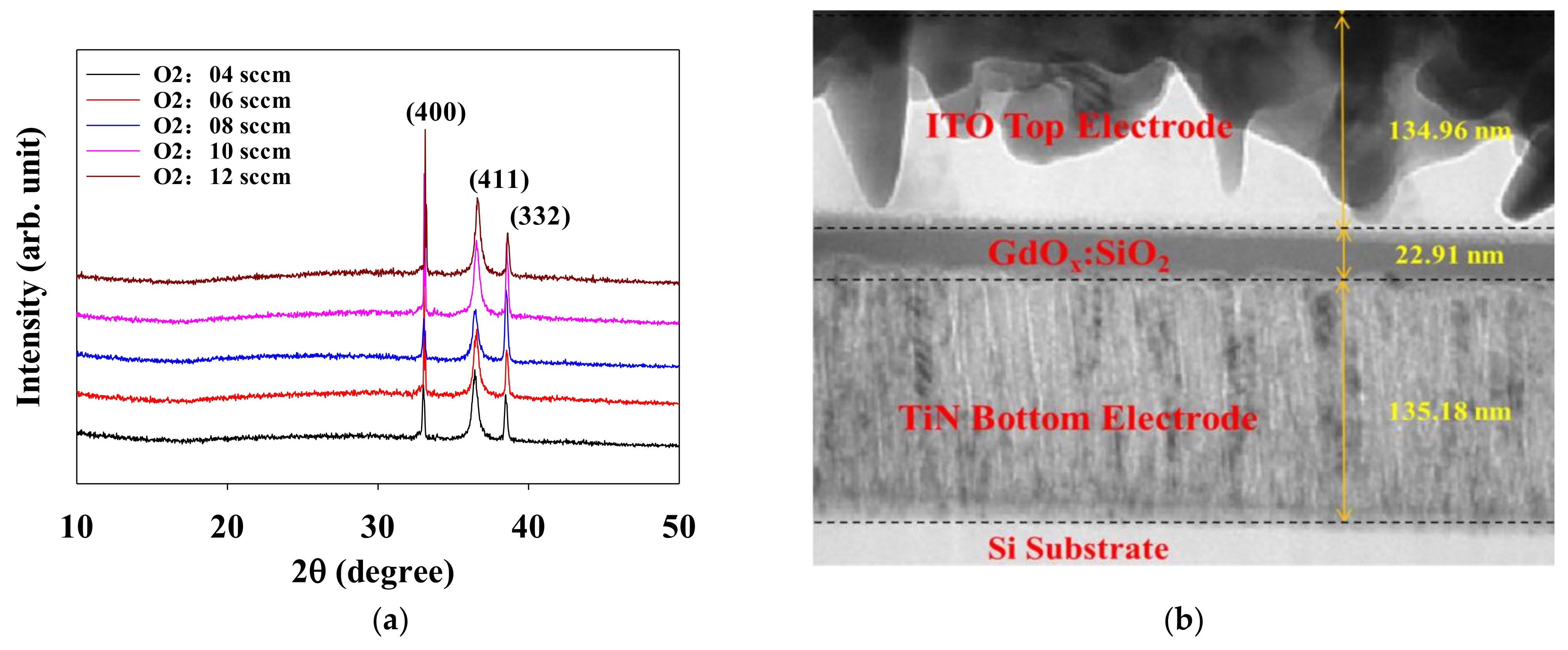
Figure 1 shows the XRD images for the co-sputtered GdOx:SiO2 thin films for 2θ of 10°–50°. For (400), (411), and (332), preferred phrase was found at 33°, 36°, and 38°, and the different GdOX thin film peaks were found and investigated. From the experimental results, it can be seen that the different GdOX thin films for different oxygen gas flow were deposited on the substrates, and no other second phase peaks were found. In Figure 2, the GdOX thin film RRAM device structures are shown in TEM cross-sectional images. The thicknesses for the TiN bottom electrode, GdOx:SiO2 thin films, and Al top electrode were calculated as 135.18 nm, 22.91 nm, and 134.9 6nm. According to a previous study, Potlog et al. reported the influence of rf sputtering power and thickness on structural and optical properties of nickel oxide thin films. The thickness and refractive index of nickel oxide thin film were increased as the rf power continuously increased [18]. In our study, thin thickness and low deposition speed of the GdOx:SiO2 thin film RRAM devices were chosen because of the high device density, low applied voltage, low power consumption, and low cost of fabrication of the investigated parameters.
Figure 1.
(a) XRD pattern and (b) the cross-sectional morphology of the GdOx:SiO2 thin films.
Figure 2.
The surface morphologies of the GdOx:SiO2 thin films for different oxygen gas flows.
Table 1 shows three different sputtering power parameters (20, 40, and 60 W) for the thin films in this paper. In addition, the inference of thin film properties was made in detail, such as the thickness as well as density of the thin films, as shown in Figure 1b. Figure 2 show the dense surface morphologies of the all GdOx:SiO2 thin films for different oxygen gas flows. The circular shape grain of the thin films was observed. The grain size of thin films were similar and caused by the low rf power deposition parameters.
Table 1.
Sputtering parameters (different rf powers).
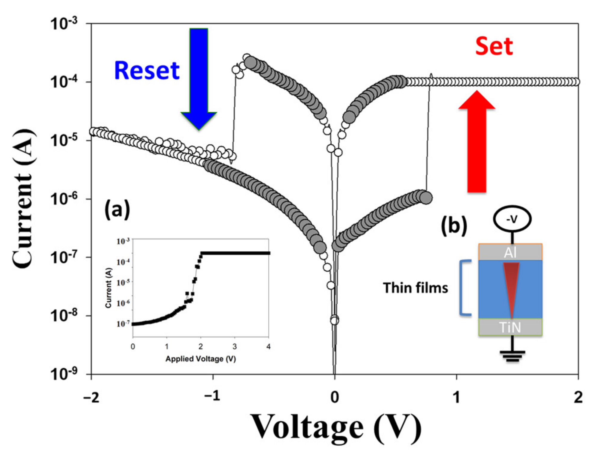
With the initial forming current increasing, the breakdown voltage of the thin film RRAM devices was obtained as 3 V. To discuss and investigate the set/reset state in the thin film RRAM devices, the operation current was continuously decreased from LRS to HRS for the negative bias applied than the reset voltage was called the reset state. In addition, the thin film RRAM devices were transferred to LRS the high positive bias than the set voltage was called the set state in Figure 3. Figure 3a exhibits the electrical forming current properties of the thin film RRAM devices, and Figure 3b shows the (ITO/GdOx:SiO2/TiN/Si) RRAM device structure.
Figure 3.
(a) the electrical forming current properties, and (b) the (ITO/GdOx:SiO2/TiN/Si) RRAM device structure for set and reset states.
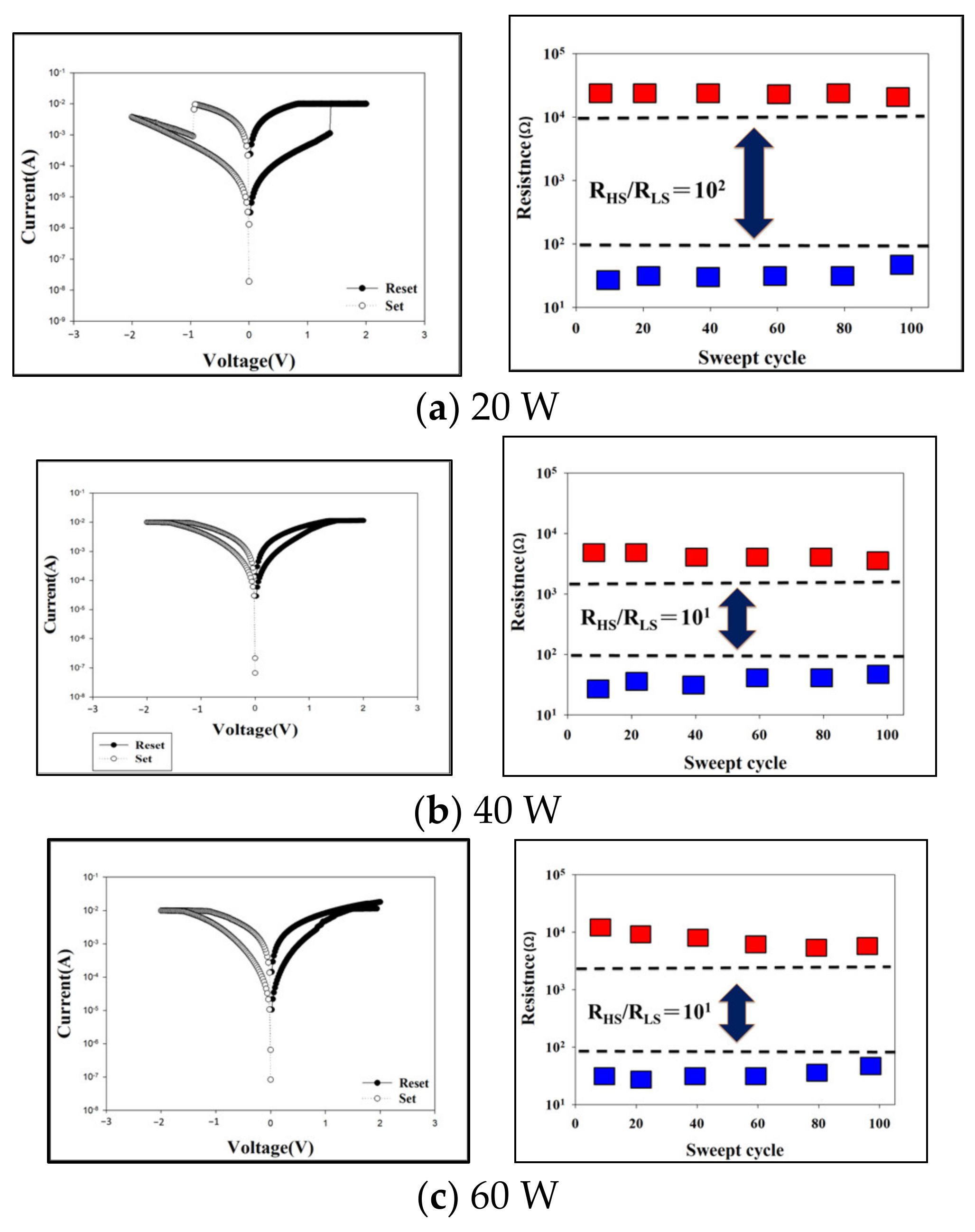
Comparing three sputtering power parameters (20, 40, 60 W), the high On/Off ratio and memory window is shown in Figure 4a. In Figure 4b, the On/Off ratio and memory window continuously became worse as the operating sweept cycle time increased. Finally, the switching properties were unstable as the operating sweept cycle time was continuously increased, as shown in Figure 4c. In conclusion, the excellent memory window of the GdOx:SiO2 thin film RRAM devices was chosen and is shown in Figure 4a for the subsequent specimens.
Figure 4.
The I−V curve characteristics and switching cycles of RRAM devices for the different rf power parameters.
With the sputtering power fixed at 20 W, the different oxygen concentration flow parameters (4, 6, 8, 10 sccm) for the sputtering process are shown in Table 2. The oxygen vacancies were filled in the oxygen gas and induced the excellent I−V curves of electrical properties of the thin films.
Table 2.
Sputtering parameters (different oxygen gas flows).
In Figure 5a, the I−V switching curves of the thin film RRAM devices exhibited the lack of oxygen atoms filled (only 4 sccm) were not obvious. When increasing the oxygen gas flow, the better I−V switching property and the switching cycle times were still unstable as shown in Figure 5b. When the oxygen gas flow was 8 sccm, better and stable switching cycle times were obtained, as shown in Figure 5c, and the oxygen vacancies filled by the oxygen gas might the main reason. Finally, when the oxygen gas flow was 10 sccm, the switching cycle times gradually became worse, and they are shown in Figure 5d. In conclusion, the excellent memory window of the GdOx:SiO2 thin film RRAM devices for 8 sccm oxygen gas flow was chosen and is shown in Figure 5c for the subsequent specimens.
Figure 5.
The I−V curve characteristics and switching cycles of RRAM devices for different O2 gas flows.
For the optimal deposition fabrication parameters of different powers and oxygen gas flows, the grain rearrangement and defects of the GdOx:SiO2 thin film RRAM devices were improved using the rapid thermal annealing (RTA) technique. In Table 3, the different specimens are divided into no-RTA, RTA 300 °C, and RTA 400 °C processing, respectively.
Table 3.
Sputtering parameters (different RTA temperatures).
To investigate the electrical transport mechanism for the initial metallic filament forming procedure, the Schottky emission conduction and the hopping conduction behavior were observed from the lnI−V and lnI-V1/2 curve fitting. The Schottky emission conduction equation is
ΦB is the Schottky barrier height, T is the absolute temperature, k is Boltzmann’s constant, εi is the insulator permittivity, and A* is the Richardson constant.
To discuss and find the ln(I/T2)-V1/2 curve, the Schottky conduction equation was fitted to the I−V curves of the GdOx:SiO2 RRAM devices. For the hopping conduction,
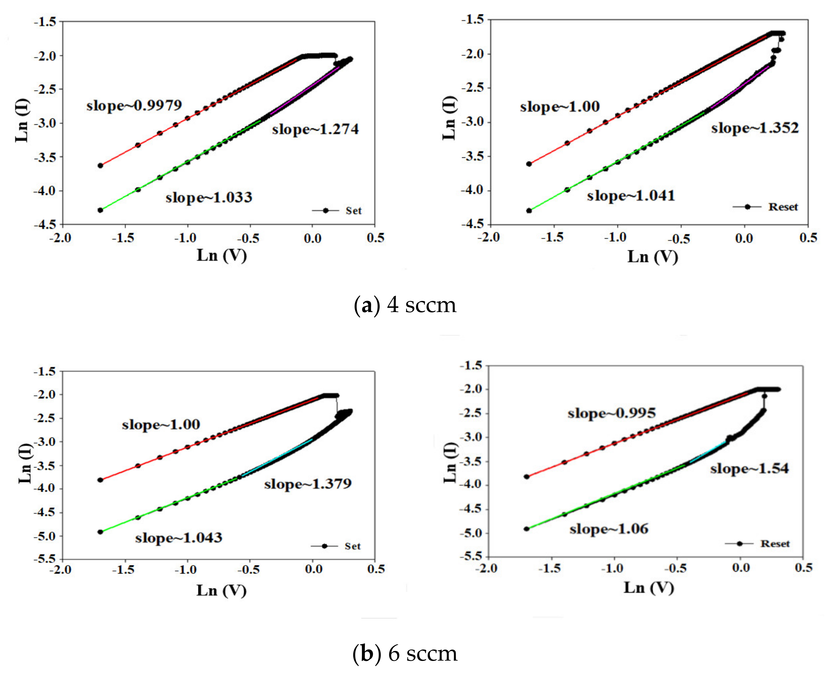
where d, ΦT, v0, N, and a are film thickness, barrier height of hopping, intrinsic vibration frequency, the density of space charge, and mean of hopping distance, respectively. To find the electrical transport mechanism for the initial metallic filament forming procedure, the ohmic conduction equation was fitted to the ln(I)–ln(V) curves of the GdOx:SiO2 RRAM devices as already widely reported [19,20,21].
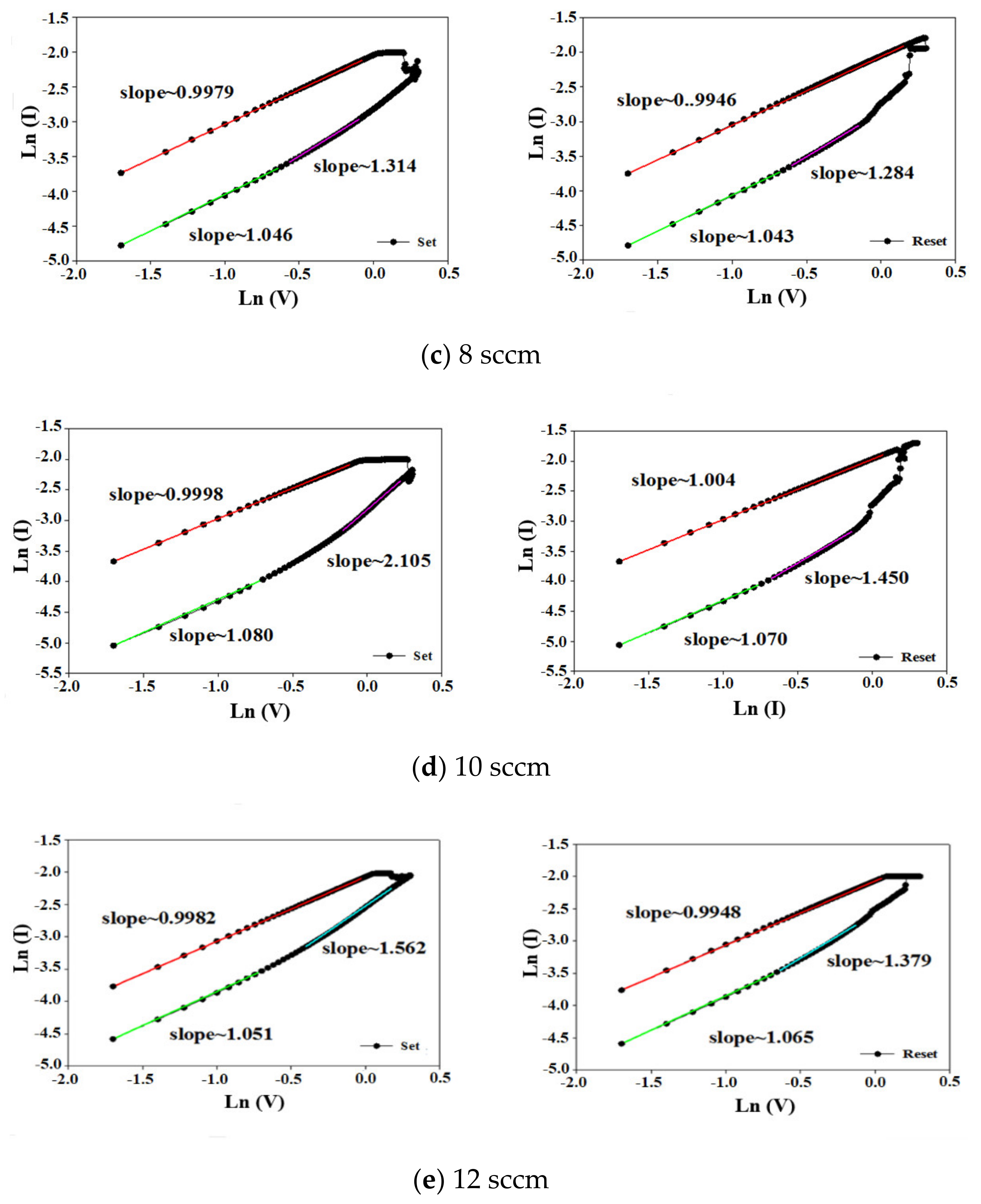
Figure 6 shows the ln(I)–ln(V) plots of ITO/GdOx:SiO2/TiN/Si RRAM devices for different oxygen gas flows. In Figure 6a, for 4 sccm oxygen gas flow, the slope of the RRAM devices for LRS/HRS states in set/reset regions can be seen and it was calculated to be about 1. The ohmic conduction transport mechanism was found from the I−V curves of the RRAM devices for low voltage and thinner film thickness were discussed. Additionally, the I−V curves of the RRAM devices for different oxygen gas flows all exhibited the ohmic conduction transport mechanism when low voltage was applied, as shown in Figure 6b–e. As shown in Figure 2, the I−V curve properties of the GdOx:SiO2 thin film RRAM devices with low applied voltage for set and reset states shows the ohmic conduction transport mechanism.

Figure 6.
Ln(I)−Ln(V) plots of ITO/GdOx:SiO2/TiN/Si RRAM for different oxygen gas flows.
Compared to the as-deposited and RTA samples in Figure 7a, the I−V switching curve properties were better and stable. When the RTA temperature increased to 400 °C, the defects became worse and the electron conduction transport behavior became difficult, and the high voltage and worse I−V switching properties of the GdOx:SiO2 thin film RRAM devices were increased and found.
Figure 7.
The I−V curve characteristics and switching cycles of RRAM devices for different RTA temperatures.
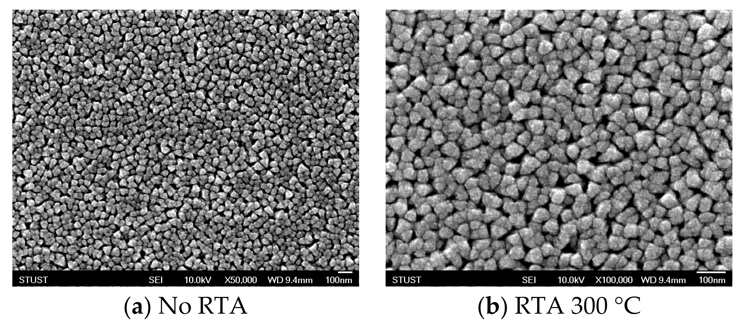
Figure 8 shows the SEM surface morphologies of co-sputtered GdOx:SiO2 thin films for no-RTA and 300 °C RTA procedures. Compared to the no-RTA specimen and 300 °C RTA, it reveals more dense and uniform grains. The average grain sizes for the no-RTA and RTA specimens were 30 nm and 50 nm, respectively.
Figure 8.
The surface morphologies of the GdOx:SiO2 thin film RRAM devices for no RTA and RTA.
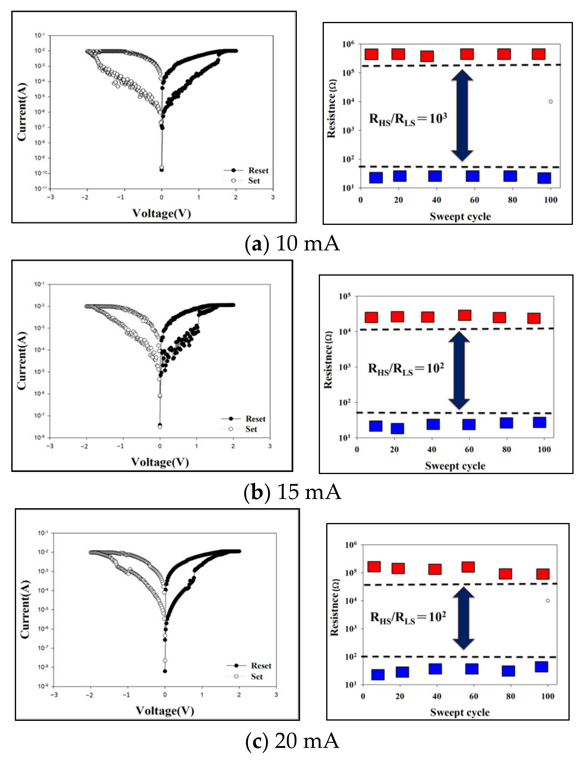
For RRAM device measurement, the current compliance was an important affective factor to causing the devices to be destroyed and broken, and the electrical conduction transport behavior of the I−V switching properties became worse. In Table 4, the current compliances are 10, 15, and 20 mA, respectively.
Table 4.
Sputtering parameters (different current compliances).
In Figure 9a, the I−V switching property of the GdOx:SiO2 thin film RRAM devices for 10 mA current compliance is stable. In Figure 9b, the memory window of RRAM devices for 15 mA current compliance is small, and low and high impedence values exhibited the low ratio. A small memory window and the sweep cycle times of the RRAM devices for higher current compliances are shown in Figure 9c. Finally, the high current compliances of 15 and 20 mA, the memory ratio and operating sweept time of the RRAM devices were worse and unstable [19,20,21].
Figure 9.
The I−V characteristics and switching cycles of the GdOx:SiO2 thin film RRAM devices for different current compliances.
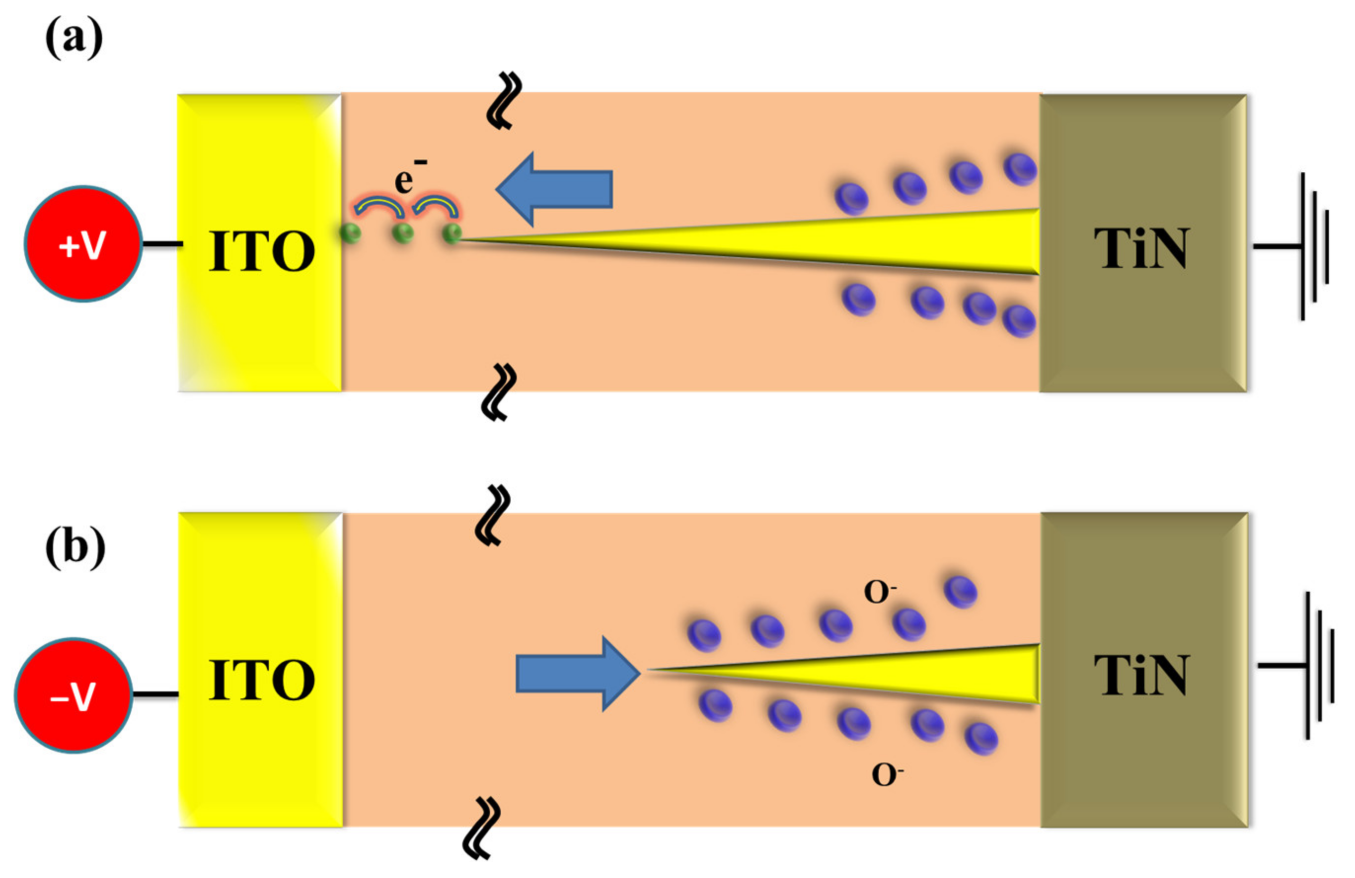
Figure 10 describes the electrical metallic filament forming procedure model of the GdOX:SiO2 thin film RRAM devices for set/reset state. In Figure 10a, the electrical metallic filament path process for the GdOX:SiO2 thin film RRAM devices for positive bias in the set state is described. In Figure 10b, the complete metal metallic filament was slightly thinner because of its continuous oxidation reaction from oxygen atoms for high negative voltage applied. The metal metallic filament was made continuously sharper by the oxygen atoms in the surface TiN bottom electrode. In addition, the resistance state of the GdOX:SiO2 thin film RRAM devices was transformed from set to reset to complete the bipolar switching process [19,20,21,22,23,24,25,26].
Figure 10.
The initial metallic filament path model of the GdOx:SiO2 thin film RRAM devices for (a) set and (b) reset state.
4. Conclusions
In this study, the co-sputtering technique was used to deposit GdOX:SiO2 thin films on TiN/Si substrates, and the ITO top electrode was then deposited and formed the ITO/GdOX:SiO2/TiN/Si RRAM device structure. Additionally, the optimal deposition parameters of a power of 20 W, oxygen gas flow of 8 sccm, RTA temperature of 300 °C, and electrical current compliance of 10 mA were found and investigated. Finally, the excellent memory window ratio and stable I−V switching properties as well as operating sweep cycle times were obtained and the optimal fabrication parameters are summarized and organized in Table 5. In summary, the GdOX:SiO2 thin film RRAM device size and thickness continuously decrease, and it has low power computation, low power loss, and small integrated device size, and the I−V curve bipolar switching properties investigated were probably cardioid and may be chosen for the next generation of semiconductor industry and product applications.
Table 5.
The optimal fabrication parameters.
Author Contributions
K.-H.C. and C.-M.C. designed and performed the experimental work, explained the obtained results, and wrote the paper. K.-H.C. and C.-M.C. conceived the study and participated in its design and coordination. K.-H.C., N.-F.W., J.-C.Z., M.-L.C. and C.-M.C. helped in writing of the paper and participated in the experimental work. All authors have read and agreed to the published version of the manuscript.
Funding
This work was performed at the National Science Council Core Facilities Laboratory for Nano-Science and Nano-Technology in the Kaohsiung-Pingtung area and was supported by the National Science Council of the Republic of China under Contract Nos. NSC MOST 110-2637-E-218-008.
Conflicts of Interest
The founding sponsors had no role in the design of the study; in the collection, analyses, or inter-pretation of data; in the writing of the manuscript, and in the decision to publish the results.
References
- Li, L.; Dai, T.; Liu, K.; Chang, K.-C.; Zhang, R.; Lin, X.; Liu, H.-J.; Lai, Y.-C.; Kuo, T.-P. Achieving complementary resistive switching and multi-bit storage goals by modulating the dual-ion reaction through supercritical fluid-assisted ammoniation. Nanoscale 2021, 13, 14035–14040. [Google Scholar] [CrossRef] [PubMed]
- Li, L.; Chang, K.-C.; Lin, X.; Lai, Y.-C.; Zhang, R.; Kuo, T.-P. Variable-temperature activation energy extraction to clarify the physical and chemical mechanisms of the resistive switching process. Nanoscale 2020, 12, 15721–15724. [Google Scholar] [CrossRef] [PubMed]
- Li, L.; Chang, K.-C.; Ye, C.; Lin, X.; Zhang, R.; Xu, Z.; Zhou, Y.; Xiong, W.; Kuo, T.-P. An indirect way to achieve comprehensive performance improvement of resistive memory: When hafnium meets ITO in an electrode. Nanoscale 2020, 12, 3267–3272. [Google Scholar] [CrossRef] [PubMed]
- Chang, K.-C.; Dai, T.; Li, L.; Lin, X.; Zhang, S.; Lai, Y.-C.; Liu, H.-J.; Syu, Y.-E. Unveiling the influence of surrounding materials and realization of multi-level storage in resistive switching memory. Nanoscale 2020, 12, 22070–22074. [Google Scholar] [CrossRef]
- Chang, K.-C.; Zhang, R.; Chang, T.-C.; Tsai, T.-M.; Chu, T.-J.; Chen, H.-L.; Shih, C.-C.; Pan, C.-H.; Su, Y.-T.; Wu, P.-J.; et al. High performance, excellent reliability multifunctional graphene oxide doped memristor achieved by self-protect ive compliance current structure. In Proceedings of the 2014 IEEE International Electron Devices Meeting (IEDM), San Francisco, CA, USA, 15–17 December 2014; pp. 33–34. [Google Scholar] [CrossRef]
- Ye, C.; Xu, Z.; Chang, K.-C.; Li, L.; Lin, X.; Zhang, R.; Zhou, Y.; Xiong, W.; Kuo, T.-P. Hafnium nanocrystals observed in a HfTiO compound film bring about excellent performance of flexible selectors in memory integration. Nanoscale 2019, 11, 20792–20796. [Google Scholar] [CrossRef] [PubMed]
- Yang, P.-C.; Chang, T.-C.; Chen, S.-C.; Lin, Y.-S.; Huang, H.-C.; Gan, D.-S. Influence of Bias-Induced Copper Diffusion on the Resistive Switching Characteristics of a SiON Thin Film. Electrochem. Solid State Lett. 2011, 14, H93–H95. [Google Scholar] [CrossRef]
- Bez, R.; Pirovano, A. Non-volatile memory technologies: Emerging concepts and new materials. Mater. Sci. Semicond. Process. 2004, 7, 349–355. [Google Scholar] [CrossRef]
- Ikegawa, S.; Mancoff, F.B.; Janesky, J.; Aggarwal, S. Magnetoresistive Random Access Memory: Present and Future. IEEE Trans. Electron Devices 2020, 67, 1407–1419. [Google Scholar] [CrossRef]
- Vorotilov, K.A.; Sigov, A.S. Ferroelectric memory. Phys. Solid State 2012, 54, 894–899. [Google Scholar] [CrossRef]
- Wong, H.S.P.; Raoux, S.; Liang, J.; Reifenberg, J.; Rajendran, B.; Asheghi, M.; Goodson, K. Phase Change Memory. Proc. IEEE 2010, 98, 2201–2227. [Google Scholar] [CrossRef]
- Shen, Z.; Zhao, C.; Qi, Y.; Xu, W.; Liu, Y.; Mitrovic, I.; Yang, L.; Zhao, C. Advances of RRAM Devices: Resistive Switching Mechanisms, Materials and Bionic Synaptic Application. Nanomaterials 2020, 10, 1437. [Google Scholar] [CrossRef]
- Chen, P.-H.; Lin, C.-Y.; Chang, T.-C. An Ultra Energy-Saving Metal/Insulator/Metal Structure for One Selector-One RRAM. In Proceedings of the 2020 IEEE International Interconnect Technology Conference (IITC), San Jose, CA, USA, 5–8 October 2020; pp. 52–54. [Google Scholar] [CrossRef]
- Patel, K.; Cottom, J.; Bosman, M.; Kenyon, A.J.; Shluger, A.L. An oxygen vacancy mediated Ag reduction and nucleation mechanism in SiO2 RRAM devices. Microelectron. Reliab. 2019, 98, 144–152. [Google Scholar] [CrossRef]
- Chen, C.Y.; Goux, L.; Fantini, A.; Redolfi, A.; Groeseneken, G.; Jurczak, M. Doped Gd-O Based RRAM for Embedded Application. In Proceedings of the 2016 IEEE 8th International Memory Workshop (IMW), Paris, France, 15–18 May 2016; pp. 1–4. [Google Scholar] [CrossRef]
- Chen, K.H.; Cheng, C.; Wang, N.; Hung, H.; Li, C.; Wu, S. First Order Rate Law Analysis for Reset State in Vanadium Oxide Thin Film Random Resist Access Memory Devices. Nanomaterials 2023, 13, 198. [Google Scholar] [CrossRef] [PubMed]
- Tsai, T.M.; Chang, K.C.; Chang, T.C.; Syu, Y.E.; Chuang, S.L. Low temperature improvement method on Zn:SiOx, resistive random access memory devices. IEEE Electron Device Lett. 2013, 34, 511–513. [Google Scholar]
- Potlog, T.; Ghimpu, L.; Suman, V.; Pantazi, A.; Enachescu, M. Influence of RF sputtering power and thickness on structural and optical properties of NiO thin films. Mater. Res. Express 2019, 6, 096440. [Google Scholar] [CrossRef]
- Chu, T.-J.; Chang, T.-C.; Tsai, T.-M.; Wu, H.-H.; Chen, J.-H.; Chang, K.-C.; Young, T.-F.; Chen, K.-H.; Syu, Y.-E.; Chang, G.-W.; et al. Charge Quantity Influence on Resistance Switching Characteristic During Forming Process. IEEE Electron Device Lett. 2013, 34, 502–504. [Google Scholar] [CrossRef]
- Chang, K.C.; Chang, T.C.; Tsai, T.M.; Zhang, R.; Hung, Y.C.; Syu, Y.E.; Chang, Y.F.; Chen, M.C.; Chu, T.J.; Chen, H.L.; et al. Physical and chemical mechanisms in oxide-based resistance random access memory. Nanoscale Res Lett. 2015, 10, 120. [Google Scholar] [CrossRef]
- Chen, K.-H.; Cheng, C.-M.; Li, C.-Y.; Huang, S.-J. Hopping conduction distance of bipolar switching GdOx resistance random access memory thin films devices modified by different constant compliance current. Microelectron. Reliab. 2018, 91, 330–334. [Google Scholar] [CrossRef]
- Sun, B.; Zhou, G.; Yu, T.; Chen, Y.; Yangb, F.; Zhao, Y. Multi-factor-controlled ReRAM devices and their applications. J. Mater. Chem. C 2022, 10, 8895–8921. [Google Scholar] [CrossRef]
- Sun, B.; Guo, T.; Zhou, G.; Ranjand, S.; Jiao, Y.; Wei, L.; Zhou, Y.; Wu, Y. Synaptic devices based neuromorphic computing applications in artificial intelligence. Mater. Today Phys. 2021, 18, 100393. [Google Scholar] [CrossRef]
- Liao, C.; Hu, X.; Liu, X.; Sun, B.; Zhou, G. Self-selective analogue FeOx-based memristor induced by the electron transport in the defect energy level. Appl. Phys. Lett. 2022, 121, 123505. [Google Scholar] [CrossRef]
- Sun, B.; Chen, Y.; Xiao, M.; Zhou, G.; Ranjan, S.; Hou, W.; Zhu, X.; Zhao, Y.; Redfern, S.; Zhou, Y.N. A Unified Capacitive-Coupled Memristive Model for the Nonpinched Current–Voltage Hysteresis Loop. Nano Lett. 2019, 19, 6461–6465. [Google Scholar] [CrossRef] [PubMed]
- Chen, K.-H.; Tsai, T.-M.; Cheng, C.-M.; Huang, S.-J.; Chang, K.-C.; Liang, S.-P.; Young, T.-F. Schottky Emission Distance and Barrier Height Properties of Bipolar Switching Gd:SiOx RRAM Devices under Different Oxygen Concentration Environments. Materials 2017, 11, 43. [Google Scholar] [CrossRef] [PubMed]
Disclaimer/Publisher’s Note: The statements, opinions and data contained in all publications are solely those of the individual author(s) and contributor(s) and not of MDPI and/or the editor(s). MDPI and/or the editor(s) disclaim responsibility for any injury to people or property resulting from any ideas, methods, instructions or products referred to in the content. |
© 2023 by the authors. Licensee MDPI, Basel, Switzerland. This article is an open access article distributed under the terms and conditions of the Creative Commons Attribution (CC BY) license (https://creativecommons.org/licenses/by/4.0/).