Abstract
The sensing mechanism of InAlN/GaN high electron mobility transistors (HEMTs) is investigated systematically by numerical simulation and theoretical analysis. In detail, the influence of additional surface charge on device performance and the dependence of surface sensing properties on InAlN barrier thickness are studied. The results indicate that the saturation output drain current Idsat and two-dimensional electron gas (2DEG) concentration increase with the increase of positive surface charge density, which decrease with the increase of negative surface charge. The influence of negative surface charge on device performance is more remarkable than that of positive surface charge. Additionally, the modulation ability of surface charge on device performance increases with the decrease ofInAlN barrier thickness. The modulation of surface charge on device performance and the influence of barrier thickness on surface sensing sensitivity are mainly attributed to the variation of the energy band structure, surface potential and 2DEG concentration in the HEMT heterostructure. This work provides important support for structural optimization design of GaN-based HEMT sensors.
1. Introduction
Due to the superior properties such as wide bandgap, high breakdown electric field, high saturation drift velocity and high thermal conductivity, GaN-based high electron mobility transistors (HEMTs) exhibit important applications in the fields of high temperature, high frequency and high power devices [1,2,3,4]. Meanwhile, two dimensional electron gas (2DEG) with a sheet concentration of as much as 1013 cm−2 is formed because of the polarization discontinuity at AlGaN (or InAlN) /GaN heterointerface. The 2DEG density strongly depends on surface states of GaN-based heterostructure. Any changes of surface state will result in changes of energy band structure and surface potential of the heterostructure. Moreover, 2DEG responds quite sensitively to any changes of the free surface charge situation. To a first approximation, for each positive or negative ion adsorbed at the free surface, accordingly, one electron is gained or lost in the 2DEG. Since the mobilities of adsorbed ions at the free surface and electrons in the 2DEG differ by many orders of magnitude, changes in the surface charge will be visible as changes in the 2DEG conductivity, however, they will be amplified by the mobility ratio. This is the basic mechanism which makes GaN-based HEMT attractive for sensor applications [5,6,7]. Recently, there are tremendous reports about AlGaN/GaN HEMT sensors for detecting gas, liquid, chemical and biomaterial, which can be used in the fields of environmental monitoring, food safety analysis and biomedicine [8,9,10,11,12]. In the past few years, researchers mainly focused on surface modification of AlGaN/GaN HEMTs for the detection of various target substances. For different targets to be tested, the best obtained result is different. For example, the highest sensing sensitivities for a pH sensor [13] and a Hg2+ ion sensor [14] are 167.71 mV/pH and 0.3 µA/ppb, respectively. Besides, there are a few studies about the methods to improve the sensing performance by optimizing HEMT device structure such as gateless structure [15,16], gate-recessed structure [17,18] and extended-gate structure [19,20]. For gateless HEMT, the sensing distance between the surface sensing area and the 2DEG channel is scaled compared to the conventional GaN-based HEMT, which makes sensing sensitivity enhanced. Due to the progress of controlling ability from the gate-recessed region, the sensing performance of the gate-recessed HEMT sensors obviously enhanced compared with the planar gate HEMT. For extended-gate HEMT, by extending the gate area and separating the sensing area from the channel of the HEMT, the device has a larger sensing area. Therefore, all of the sensing sensitivity, stability and detection limit of the HEMT sensors are improved.
In fact, to further improve the sensing performance of GaN-based HEMTs effectively, it is necessary to investigate the sensing mechanism comprehensively. Until now, there are few reports about the sensing mechanism of GaN-based HEMT. Besides, owing to the relatively mature epitaxial and manufacturing technology, the heterostructure mainly used for HEMT sensors in the past few years is AlGaN/GaN. Compared with conventional AlGaN/GaN heterostructure, the lattice-matched In0.17Al0.83N/GaN heterostructure, has higher carrier concentration and better 2DEG confinement [21,22]. In fact, lattice-matched In0.17Al0.83N/GaN heterostructure is more suitable for HEMT sensors. However, there are only a few reports about InAlN/GaN HEMT sensors [23,24]. In this work, the modulation law of surface charge on the device performance and the effect of InAlN barrier layer thickness on the sensing performance of InAlN/GaN HEMT are studied systematically, which is considered to provide a broad-version route map for designing InAlN based HEMT sensors.
2. Device Structure and Theoretical Models
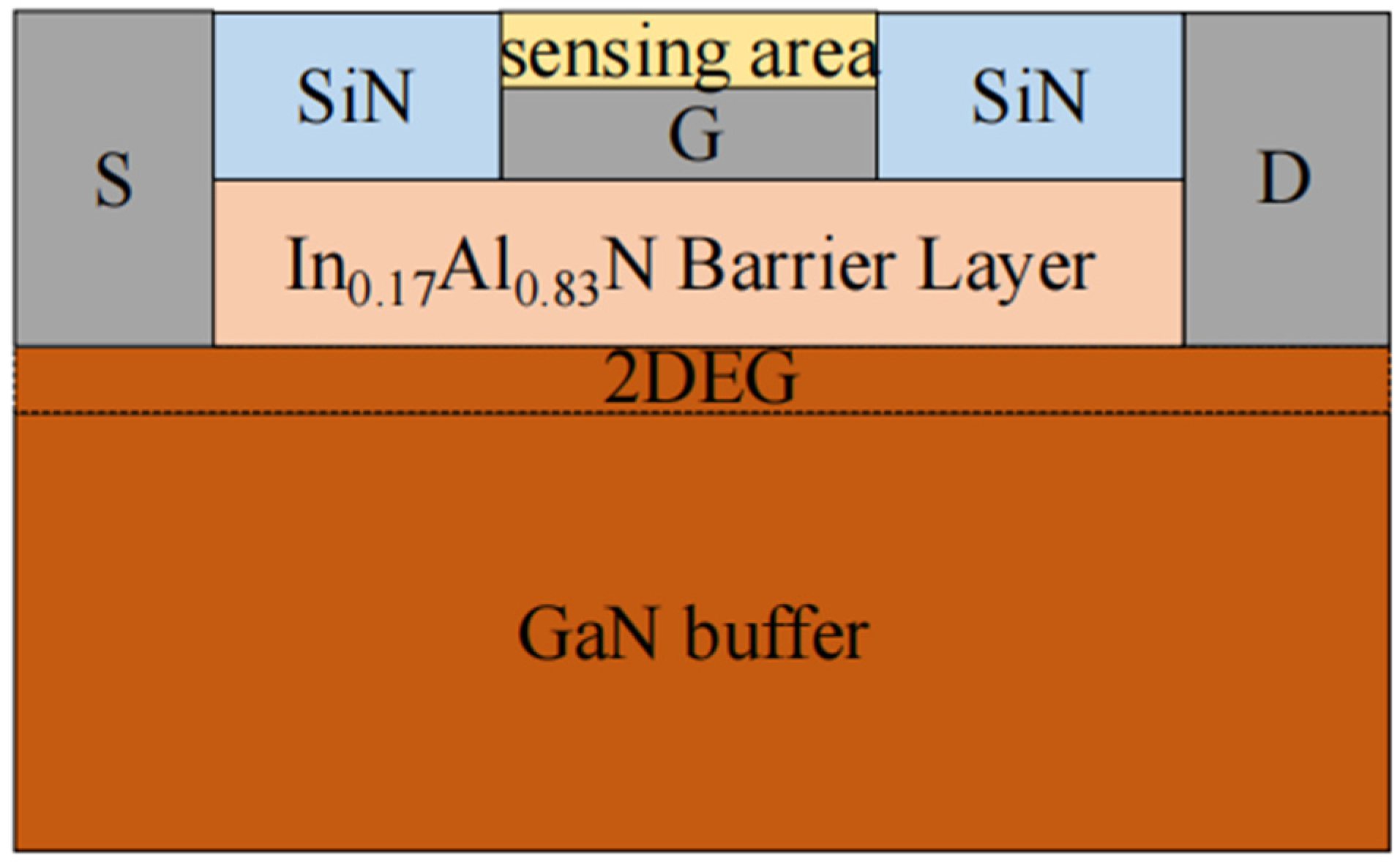
The InAlN/GaN HEMT device structure used in this study is shown in Figure 1. The HEMT heterostructure on sapphire substrate consists of a 2-μm-thick GaN buffer layer and a thin In0.17Al0.83N barrier layer. A SiN passivation layer was applied between the gate sensing area and ohmic contacts (source and drain electrodes). To be close to the real experiment, the n-type doping densities in both GaN buffer layer and InAlN barrier layer used in this work were set to be 1 × 1016 cm−3, due to the fact that the unintentionally doping InAlN/GaN heterostructures grown in the experiment exhibit n-type doping with a concentration of 1 × 1016 cm−3. The distance between the source and drain electrodes is 3 μm. The length of the sensing area for gate region is 1.5 μm.
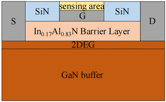
Figure 1.
Schematic diagram of the InAlN/GaN HEMT.
To obtain the Idsat, 2DEG concentration and the energy band profile of the HEMT with varying surface charge, the Schrödinger equation, Poisson’s equation and the carrier continuity equation are solved self-consistently [25,26]. The equations can be expressed as follows, respectively.
Schrödinger equation:
where ħ is the Planck’s constant, m* is the effective mass of the electron, V(z) is the potential energy of the electron, E is the energy of the electron and ψ is the wave function. Poisson’s equation:
where ε is the dielectric constant, ϕ(z) is the electrostatic potential, q is the charge, is the dissociative sender concentration and n is the electron concentration. Since the contribution of the acceptor charge as well as the holes on the total charge are very small, the acceptor charge and holes are neglected in the calculation.
Carrier continuity equation:
where Jn is the electron current density, Gn is the electron production rate and Rn is the electron complex rate.
The self-consistent procedure is that the potential V is obtained using Poisson’s equation from an initial guess of the mobile charge concentration, and then inserted into the Schrödinger equation, which is solved to obtain the energy levels and wavefunctions of the systems. The new electron charge density is then calculated by applying Fermi statistics
where EF is Fermi level, Ei is energy of the ith quantized level, T is temperature and KB is Boltzmann’s constant.
The calculated density is then plugged into Poisson’s equation and the iteration repeated until convergence is achieved.
The polarization model, Shockley–Read-Hall recombination model and Albrecht model incorporated for concentration dependent low field mobility were incorporated in the simulations study through Silvaco TCAD [27]. We applied a fixed temperature of 300 K due to the neglecting self-heating effect when the device is operated at low biases. The electron transport was also included based on a drift-diffusion model [28,29]. In the simulation, we set the value of saturation velocity and the parameters of electron and hole recombination lifetimes (taun0 and taup0) in SRH recombination model. Besides, we adopted the parameters for GaN, InN, and AlN that Braga et al. [30] have reported such as energy band structure, spontaneous polarization, mobilities and saturation velocities. Linear interpolations are adopted to compute parameter values as a function of mole fraction in InAlN.
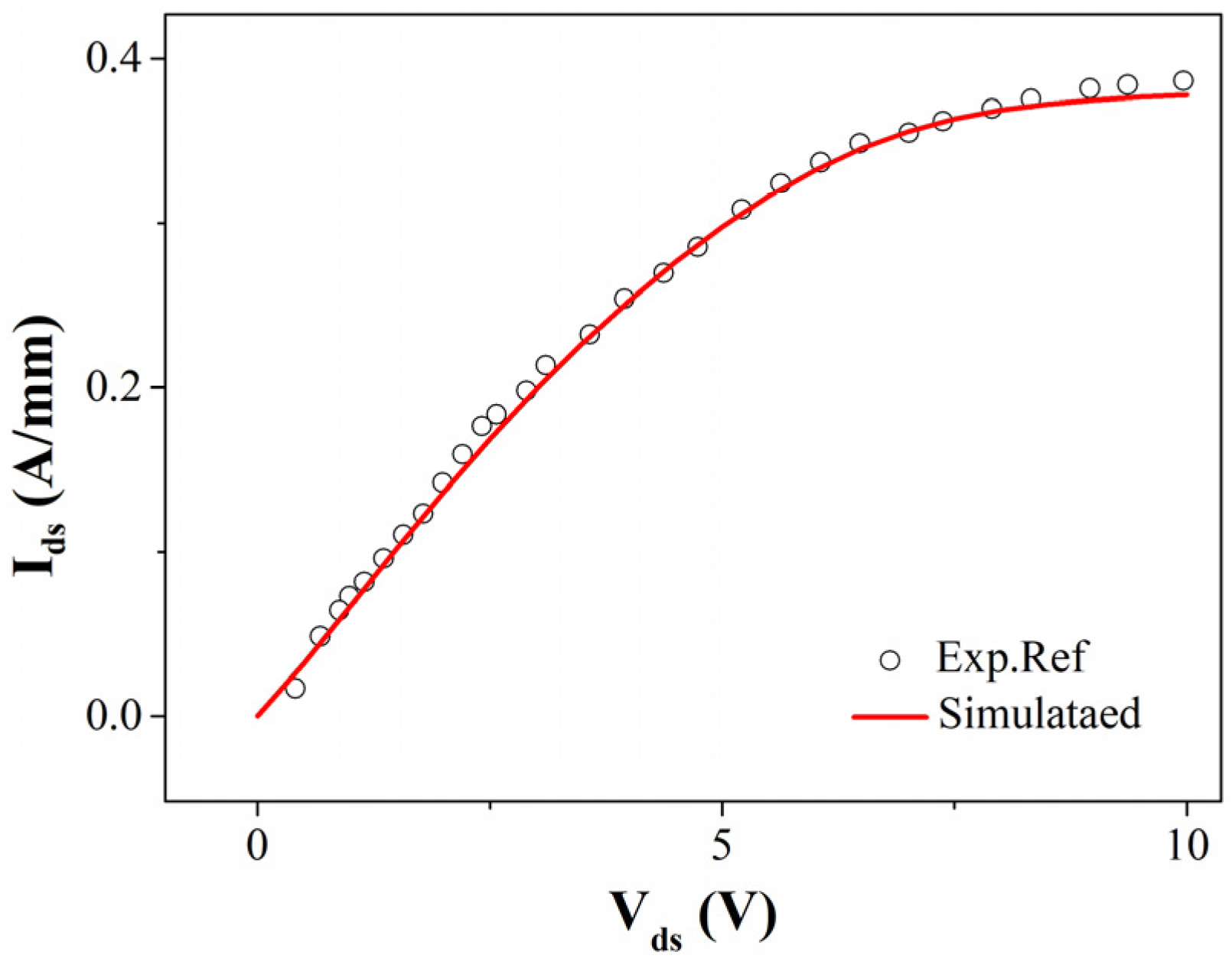
To verify the validity of the simulation results in this work, we compare the simulation results with previous experimental report. As shown in Figure 2, simulated DC current of InAlN/GaN HEMT without additional surface charge is basically matched to the experimental results of the same structure [31,32].
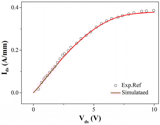
Figure 2.
Output characteristics of InAlN/GaN HEMT from simulation and experimental results.
3. Results and Discussion
3.1. Influence of Surface Charge on Device Performance of InAlN/GaN HEMTs
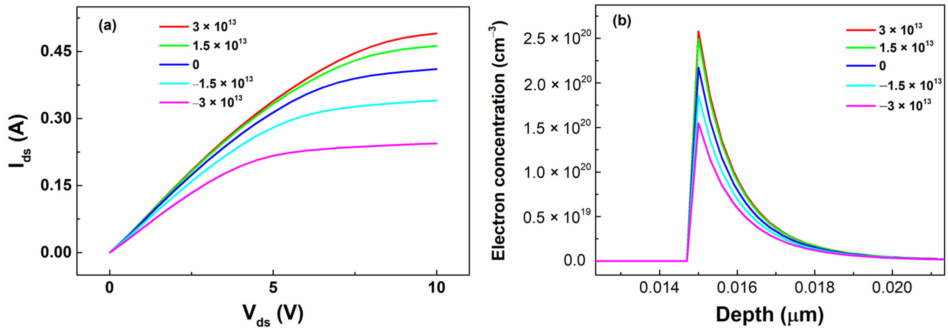
Figure 3 shows the output characteristics and carrier concentration distributions of the InAlN/GaN HEMT with different surface charge density. As shown in Figure 3a, the saturation drain current Idsat increases with the increase of positive surface charge density and decreases with the increase of negative surface charge density. The influence of negative surface charge on device performance is more significant than that of positive charge. In fact, the effect of surface charge on the Idsat mainly resulted from the changes of 2DEG concentration. The carrier concentration distributions of the HEMT under gate region with different surface charge density are shown in Figure 3b. Corresponding to the change of Idsat, the 2DEG concentration increases with the increase of positive surface charge, which decreases with the increase of negative surface charge.

Figure 3.
(a) The output characteristics and (b) carrier concentration distributions of the HEMT with different surface charge density at Vg = 0 V.
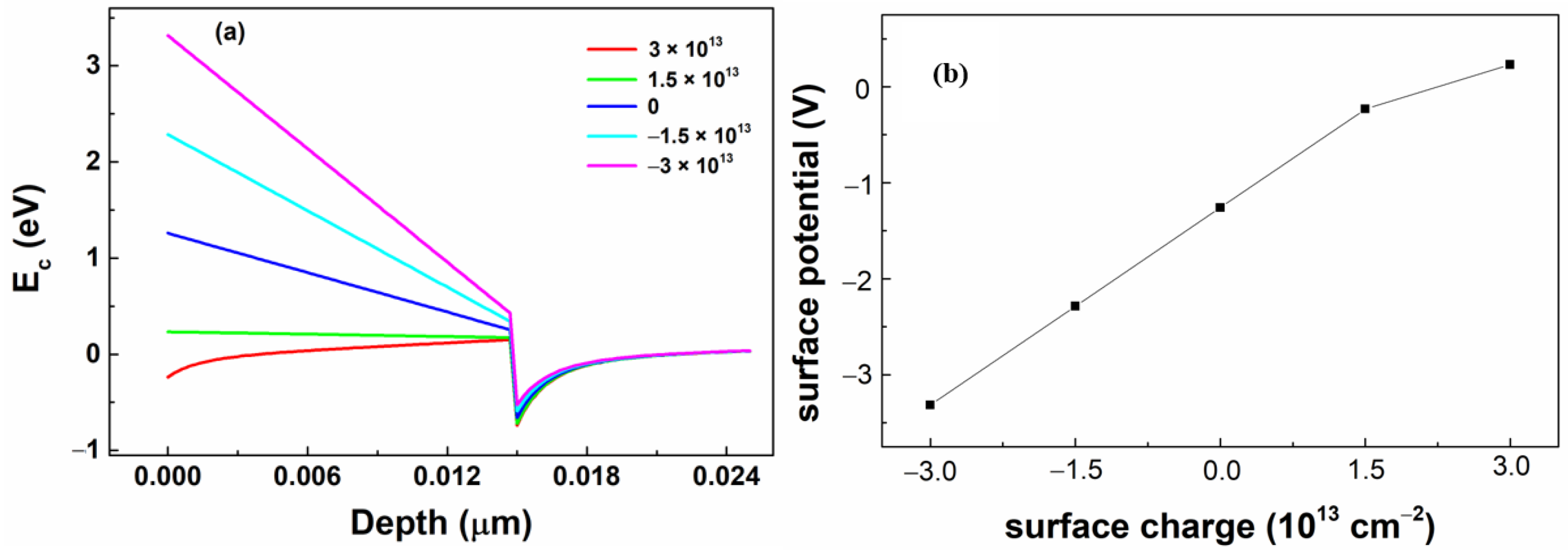
The intrinsic physical reason for the changes of Idsat and 2DEG concentration with surface charge can be mainly attributed to the effect of the energy band structure and surface potential of the InAlN/GaN HEMT heterostructure. The conduction band diagram of the HEMT under gate region with different surface charge density is shown in Figure 3a. The corresponding surface potential representing energy difference between the conduction band edge of surface and Fermi level EF is shown in Figure 3b. Considering the energy band diagram of the HEMT as sketched in Figure 3, the sheet charge density NS can be written as [33]
where dbarrier is the barrier thickness, q is the elementary charge, ΦS is the surface potential, EF is the Fermi level at the interface relative to the bottom of the GaN conduction band and ΔEC is the conduction band offset between InAlN barrier layer and GaN buffer.
As shown in Figure 4, the surface potential of InAlN/GaN HEMT heterostructure under gate region increases slightly with positive surface charge. Correspondingly, the depth of triangular quantum potential well at InAlN/GaN interface becomes deeper, which enhanced the 2DEG confinement. So, the 2DEG concentration and Idsat increase with the increase of positive surface charge density. As the negative surface charge density increases, the surface potential decreases and the depth of the triangular potential well becomes shallower, which weakens the confinement of the 2DEG at InAlN/GaN interface. So, the 2DEG concentration and Idsat will decrease. In fact, the simulated sensing rule in this work is consistent with a previous experiment report that the output current of HEMT device decreases gradually as the pH value increases [11]. For HEMT pH sensor, the drain current decreased with increased pH value, because the adsorbed negative charges on HEMT sensing area increases with pH value.
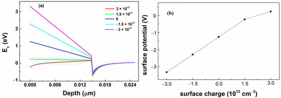
Figure 4.
(a) The conduction band diagram and (b) surface potential of the HEMT under the gate region with different surface charge density.
3.2. The Effect of InAlN Barrier Thickness on the Sensing Performance of InAlN/GaN HEMT Device
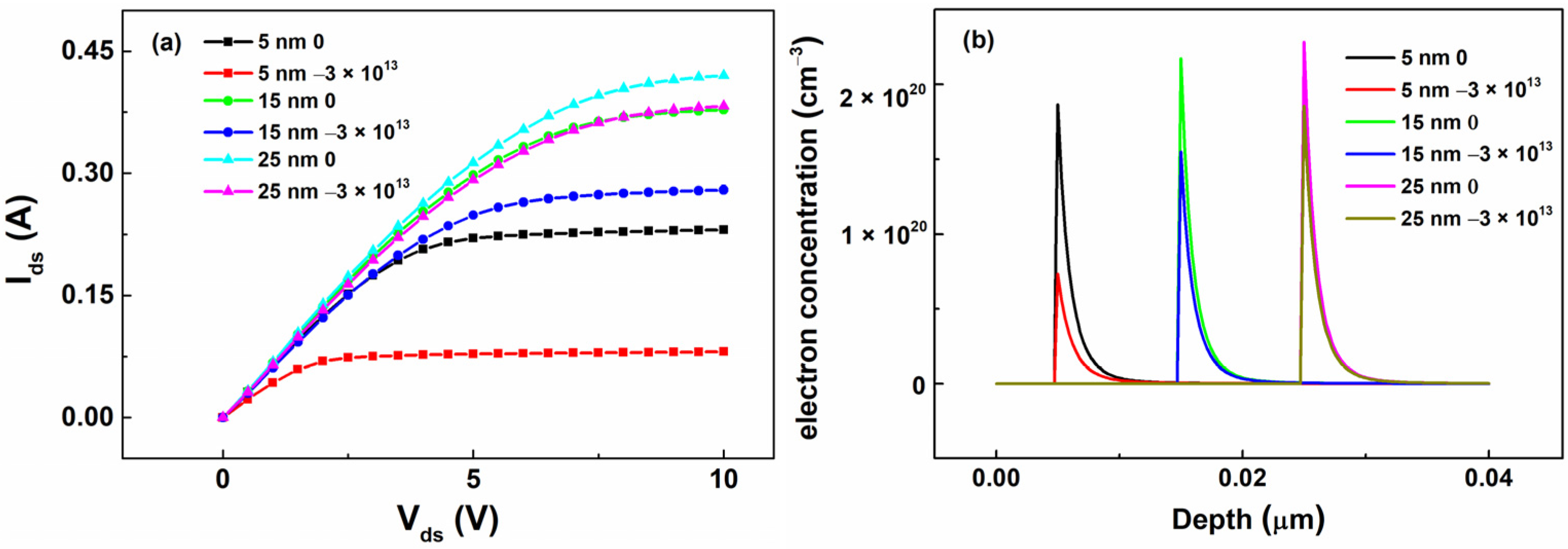
To further study the surface sensing properties of HEMT, the effect of the InAlN barrier thickness on the surface sensing performance of InAlN/GaN HEMT devices is investigated by comparing the device performance before and after adding the same density of surface charges (σS = –3 × 1013 cm−2). The InAlN barrier thicknesses ranged from 5 to 25 nm. Figure 5 shows the output characteristics and 2DEG concentration distributions of HEMT for varying InAlN thickness with and without additional surface charge. As shown in Figure 5, with the increase of barrier layer thickness, the Idsat and 2DEG concentration increase when the additional surface charge is zero, which can be deduced from the energy band diagram [34,35]. Correspondingly, the energy drop in the barrier layer increases, leading to a deeper triangular quantum well at the hetero-interface. In further, the confinement of the quantum well on 2DEG is enhanced. Consequently, the 2DEG concentration and drain current also increase with the increase of barrier layer thickness.

Figure 5.
(a) The output characteristics and (b) carrier concentration distributions of HEMT with surface charge on the structure at different InAlN barrier layer thicknesses.
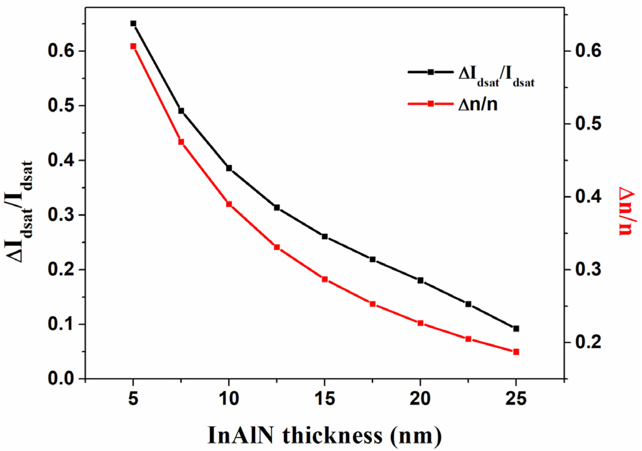
Additionally, from Figure 5 we can get the variation quantity of the saturation current ΔIdsat and 2DEG concentration Δn before and after adding the same density surface charges for various InAlN thicknesses. The change rates of the ΔIdsat/Idsat and the Δn/n are shown in Figure 6. In contrast to the variation of the Idsat and 2DEG concentration, the ΔIdsat, ΔIdsat/Idsat, Δn and Δn/n decrease gradually with the increase of InAlN thickness for HEMT. The change rates of the ΔIdsat/Idsat are approximately in the range of 0.1–0.65.
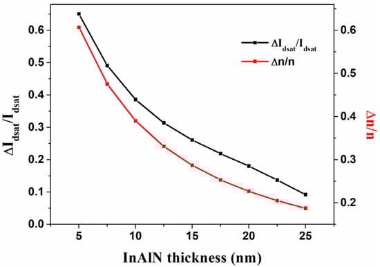
Figure 6.
The change rates of the saturation drain current and the 2DEG concentration of the HEMT with different InAlN barrier thicknesses.
From the above results, it can be confirmed that the influence of surface charge on device performance increases with the decrease of the InAlN barrier thickness, which means that the modulation ability of surface charge on device performance will be increased by decreasing the InAlN thickness. So, we can conclude that the surface sensing sensitivity can be enhanced by thinning the barrier layer thickness in a certain range, when GaN-based HEMT is used as sensor.
The intrinsic physical mechanism for the above phenomenon and results is still resulted from the changes of the energy band structure and surface potential of the InAlN/GaN HEMT heterostructure. Figure 7 shows the energy band diagram of the HEMT under the gate region with and without additional surface charge for various InAlN barrier thicknesses. It can be seen from the diagram that with the increase of InAlN barrier thickness, the depth difference of the triangular potential well before and after additional surface charge decreases due to the enlarged distance between the sensing area and the 2DEG channel. Therefore, the influence of the same density surface charge on the interface potential well increases with the decrease of InAlN barrier thickness, which in turn affects the output characteristics and 2DEG concentration of the HEMT. So, the modulation ability of surface charge on device Idsat and the 2DEG concentration increase with the decrease of InAlN thickness, which means that the sensing sensitivity of GaN-based HEMT sensor can be improved by thinning the barrier layer.
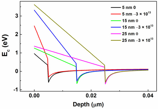
Figure 7.
The conduction band diagram of HEMT for different InAlN barrier layer thicknesses with and without additional surface charge density.
4. Conclusions
In this work, the sensing mechanism of InAlN/GaN HEMT and the dependence of the sensing sensitivity on the InAlN barrier layer thickness were studied by solving the Schrodinger equation, Poisson’s equation and the carrier continuity equation self-consistently. The results exhibit that both the Idsat and 2DEG concentration increase with the increase of positive surface charge, which decrease with the increasing negative charge. The influence of negative surface charge on device performance is more significant than that of positive surface charge. This can be attributed to the change of the energy band structure and surface potential of HEMT with varying surface charge density. Moreover, the Idsat and 2DEG concentration increase with the increase of InAlN barrier thickness, while the modulation ability of surface charge on device performance will decrease due to the enlarged distance between the sensing area and 2DEG channel. This means that the sensing sensitivity will decrease. So, when GaN-based HEMT is used as surface ion sensors, the barrier layer thickness should be as thin as possible.
Author Contributions
Conceptualization, Y.L. (Yanli Liu) and D.C.; formal analysis, X.H. and Y.D.; investigation, S.F. and Y.L. (Yuhui Liu); writing—original draft preparation, Y.L. (Yanli Liu); writing—review and editing, D.C. All authors have read and agreed to the published version of the manuscript.
Funding
This research was funded by the National Nature Science Foundation of China, grant number 61804089; Shandong Provincial Science and Technology Support Program of Youth Innovation Team in College, grant numbers 2019KJN041 and 2020KJN005; Basic Research Project of the Basic Research Business of the Provincial University in Heilongjiang Province, grant number 2021-KYYWF-0036; and the PhD Start-up Fund of Shandong Technology and Business University, grant number (BS201608).
Institutional Review Board Statement
Not applicable.
Informed Consent Statement
Not applicable.
Data Availability Statement
Not applicable.
Conflicts of Interest
The authors declare no conflict of interest.
References
- Palacios, T.; Chakraborty, A.; Rajan, S.; Poblenz, C.; Keller, S.; DenBaars, S.P.; Speck, J.S.; Mishra, U.K. High-power AlGaN/GaN HEMTs for ka-band applications. IEEE Electron. Device Lett. 2005, 26, 781–783. [Google Scholar] [CrossRef] [Green Version]
- Driad, S.B.; Maher, H.; Defrance, N.; Hoel, V.; De Jaeger, J.C.; Renvoise, M.; Frijlink, P. AlGaN/GaN HEMTs on Silicon Substrate With 206-GHz FMAX. IEEE Electron. Device Lett. 2013, 34, 36–38. [Google Scholar] [CrossRef]
- Xu, R.; Chen, P.; Liu, M.H.; Zhou, J.; Li, Y.M.; Cheng, K.; Liu, B.; Chen, D.J.; Xie, Z.L.; Zhang, R.; et al. 3.4-kV AlGaN/GaN Schottky Barrier Diode on Silicon Substrate With Engineered Anode Structure. IEEE Electron. Device Lett. 2021, 42, 208–211. [Google Scholar] [CrossRef]
- Fitch, R.C.; Walker, D.E.; Green, A.J.; Tetlak, S.E.; Gillespie, J.K.; Gilbert, R.D.; Sutherlin, K.A.; Gouty, W.D.; James, P.; Theimer, J.P.; et al. Implementation of High-Power-Density X-Band AlGaN/GaN High Electron Mobility Transistors in a Millimeter-Wave Monolithic Microwave Integrated Circuit Process. IEEE Electron. Device Lett. 2015, 36, 1004–1007. [Google Scholar] [CrossRef]
- Sharma, N.; Mishra, S.; Singh, K.; Chaturvedi, N.; Chauhan, A.; Periasamy, C.; Kharbanda, D.K.; Parjapat, P.; Khanna, P.K.; Chaturvedi, N. High-resolution AlGaN/GaN HEMT-based electrochemical sensor for biomedical applications. IEEE Trans. Electron. Devices 2019, 67, 289–295. [Google Scholar] [CrossRef]
- Ibbetson, J.P.; Fini, P.T.; Ness, K.D.; DenBaars, S.P.; Speck, J.S.; Mishra, U.K. Polarization effects, surface states, and the source of electrons in AlGaN/GaN heterostructure field effect transistors. Appl. Phys. Lett. 2000, 77, 250–252. [Google Scholar] [CrossRef]
- Ould-Abbas, A.; Zeggaia, O.; Bouchaour, M.; Zeggai, H.; Sahouane, N.; Madani, M.; Trari, D.; Boukais, M.; Chabane-Sari, N.E. Study on functionalizing the surface of AlGaN/GaN high electron mobility transistor based sensors. J. Optoelectron. Adv. Mater. 2013, 15, 1323–1327. [Google Scholar]
- Ahn, J.; Kim, D.; Park, K.H.; Yoo, G.; Heo, J. Pt-decorated graphene gate AlGaN/GaN MIS-HEMT for ultrahigh sensitive hydrogen gas detection. IEEE Trans. Electron. Devices 2021, 68, 1255–1261. [Google Scholar] [CrossRef]
- Chaturvedi, N.; Singh, K.; Kachhawa, P.; Lossy, R.; Wuerfl, J. AlGaN/GaN HEMT based sensor and system for polar liquid detection. Sens. Actuators A Phys. 2020, 302, 111799. [Google Scholar] [CrossRef]
- Woo, K.; Kang, W.; Lee, K.; Lee, P.; Kim, Y.; Yoon, T.S.; Cho, C.Y.; Park, K.H.; Ha, M.W.; Lee, H.H. Enhancement of cortisol measurement sensitivity by laser illumination for AlGaN/GaN transistor biosensor. Biosens. Bioelectron. 2020, 159, 112186. [Google Scholar] [CrossRef]
- Dong, Y.; Son, D.H.; Dai, Q.; Lee, J.H.; Won, C.H.; Kim, J.G.; Chen, D.J.; Lee, J.H.; Lu, H.; Zhang, R.; et al. High sensitive pH sensor based on AlInN/GaN heterostructure transistor. Sensors 2018, 18, 1314. [Google Scholar] [CrossRef] [PubMed] [Green Version]
- Varghese, A.; Periasamy, C.; Bhargava, L. Fabrication and charge deduction based sensitivity analysis of GaN MOS-HEMT device for glucose, MIG, C-erbB-2, KIM-1, and PSA detection. IEEE Trans. Nanotechnol. 2019, 18, 747–755. [Google Scholar] [CrossRef]
- Cho, S.K.; Cho, W.J. High-Sensitivity pH sensor based on coplanar gate AlGaN/GaN metal-oxide-semiconductor high electron mobility transistor. Chemosensors 2021, 9, 42. [Google Scholar] [CrossRef]
- Nigam, A.; Sharma, N.; Tripathy, S.; Kumar, M. Development of semiconductor based heavy metal ion sensors for water analysis: A review. Sens. Actuators A Phys. 2021, 330, 112879. [Google Scholar] [CrossRef]
- Sokolovskij, R.; Zheng, H.Z.; Li, W.M.; Zhou, G.N.; Wang, Q.; Zhang, G.Q.; Yu, H.Y. Application of a gateless AlGaN/GaN HEMT sensor for diesel soot particulate detection. Sens. Actuators B Chem. 2021, 349, 130811. [Google Scholar] [CrossRef]
- Jia, X.L.; Chen, D.J.; Liu, L.; Lu, H.; Zhang, R.; Zheng, Y.D. Highly selective and sensitive phosphate anion sensors based on AlGaN/GaN high electron mobility transistors functionalized by ion imprinted polymer. Sci. Rep. 2016, 6, 27728. [Google Scholar] [CrossRef] [PubMed]
- Sokolovskij, R.; Zhang, J.; Zheng, H.; Li, W.M.; Jiang, Y.; Yang, G.Y.; Yu, H.Y.; Sarro, P.M.; Zhang, G.Q. The Impact of Gate Recess on the H2; Detection Properties of Pt-AlGaN/GaN HEMT Sensors. IEEE Sens. J. 2020, 20, 8947–8955. [Google Scholar] [CrossRef]
- Lee, C.T.; Chiu, Y.S. Gate-recessed AlGaN/GaN ISFET urea biosensor fabricated by photoelectrochemical method. IEEE Sens. J. 2015, 16, 1518–1523. [Google Scholar] [CrossRef]
- Ding, X.Z.; Miao, B.; Gu, Z.Q.; Wu, B.J.; Hu, Y.M.; Wang, H.; Zhang, J.; Wu, D.M.; Lu, W.H.; Li, J.D. Highly sensitive extended gate-AlGaN/GaN high electron mobility transistor for bioassay applications. RSC Adv. 2017, 7, 55835–55838. [Google Scholar] [CrossRef] [Green Version]
- Pyo, J.Y.; Jeon, J.H.; Koh, Y.; Cho, C.Y.; Park, H.H.; Park, K.H.; Lee, S.W.; Cho, W.J. AlGaN/GaN high-electron-mobility transistor pH sensor with extended gate platform. AIP Adv. 2018, 8, 85106. [Google Scholar] [CrossRef] [Green Version]
- Hao, Y.; Xue, J.S.; Zhang, J.C. Research progress in the group-III nitride InAlN semiconductorheterostructures. Sci. China Inform. Sci. 2012, 42, 1577–1587. [Google Scholar]
- Tülek, R.; Ilgaz, A.; Gökden, S.; Teke, A.; Öztürk, M.K.; Kasap, M.; Özçelik, S.; Arslan, E.; Özbay, E. Comparison of the trans-port properties of high quality AlGaN/AlN/GaN and AlInN/AlN/GaN two-dimensional electron gas heterostructures. J. Appl. Phys. 2009, 105, 13707. [Google Scholar] [CrossRef] [Green Version]
- Jia, X.L.; Huang, X.Y.; Yin, T.; Yang, L.H.; Chen, D.J. Ultrasensitive Detection of Phosphate Using Ion-Imprinted Polymer Functionalized AlInN/GaN High Electron Mobility Transistors. IEEE Electron. Device Lett. 2016, 37, 913–915. [Google Scholar] [CrossRef]
- Chapin, C.A.; Miller, R.A.; Dowling, K.M.; Chen, R.Q.; Senesky, D.G. InAlN/GaN high electron mobility micro-pressure sensors for high-temperature environments. Sens. Actuator A Phys. 2017, 263, 216–223. [Google Scholar] [CrossRef]
- Kong, Y.C.; Zheng, Y.D.; Chu, R.M.; Gu, S.L. Influence of Al-content on the property of the two-dimensional electron gases in AlxGa1-xN/GaN heterostructures. Acta Phys. Sin. 2003, 52, 1756–1760. [Google Scholar] [CrossRef]
- Amarnath, G.; Panda, D.K.; Lenka, T.R. Modeling and simulation of DC and microwave characteristics of AlInN (AlGaN)/AlN/GaN MOSHEMTs with different gate lengths. Int. J. Numer. Modell. Electron. Netw. Devices Fields 2019, 32, e2456. [Google Scholar] [CrossRef] [Green Version]
- Mohammadzamani, M.; Fathipour, M. An investigation of highly scaled III-nitride Gallium-face and Nitrogen-face HEMTs. Superlattices Microstruct. 2015, 78, 125–133. [Google Scholar] [CrossRef]
- Albrecht, J.D.; Wang, R.P.; Ruden, P.P.; Farahmand, M.; Brennan, K.F. Electron transport characteristics of GaN for high temperature device modeling. J. Appl. Phys. 1998, 83, 4777–4781. [Google Scholar] [CrossRef]
- Chang, Y.; Tong, K.Y.; Surya, C. Numerical simulation of current–voltage characteristics of AlGaN/GaN HEMTs at high temperatures. Semicond. Sci. Technol. 2005, 20, 188. [Google Scholar] [CrossRef]
- Braga, N.; Mickevicius, R.; Gaska, R.; Hu, X.; Shur, M.S.; Khan, M.A.; Simin, G.; Yang, J. Simulation of hot electron and quantum effects in AlGaN/GaN heterostructure field effect transistors. J. Appl. Phys. 2004, 95, 6409–6413. [Google Scholar] [CrossRef] [Green Version]
- Higashiwaki, M.; Matsui, T. MBE growth and device characteristics of InAlN/GaN HFETs. Phys. Status Solidi C 2005, 2, 2598–2601. [Google Scholar] [CrossRef]
- Kanaga, S.; Dutta, G.; Kushwah, B.; DasGupta, N.; DasGupta, A. Low Temperature and High Pressure Oxidized Al2O3 as Gate Dielectric for AlInN/GaN MIS-HEMTs. IEEE Trans. Device Mater. Reliab. 2020, 20, 613–621. [Google Scholar] [CrossRef]
- Ambacher, O.; Smart, J.; Shealy, J.R.; Weimann, N.G.; Chu, K.; Murphy, M.; Schaff, W.J.; Eastman, L.F.; Dimitrov, R.; Wittmer, L.; et al. Two-dimensional electron gases induced by spontaneous and piezoelectric polarization charges in N-and Ga-face AlGaN/GaN heterostructures. J. Appl. Phys. 1999, 85, 3222–3233. [Google Scholar] [CrossRef] [Green Version]
- Jogai, B. Influence of surface states on the two-dimensional electron gas in AlGaN/GaN heterojunction field-effect transistors. J. Appl. Phys. 2003, 93, 1631–1635. [Google Scholar] [CrossRef]
- Behmenburg, H.; Khoshroo, L.R.; Eickelkamp, M.; Mauder, C.; Fieger, M.; Ketteniss, N.; Woitok, J.; Wamwangi, D.; Wuttig, M.; Hernandez, S.E.; et al. Influence of barrier thickness on AlInN/AlN/GaN heterostructures and device properties. Phys. Status Solidi C 2009, 6, S1041–S1044. [Google Scholar] [CrossRef]

Publisher’s Note: MDPI stays neutral with regard to jurisdictional claims in published maps and institutional affiliations. |
© 2022 by the authors. Licensee MDPI, Basel, Switzerland. This article is an open access article distributed under the terms and conditions of the Creative Commons Attribution (CC BY) license (https://creativecommons.org/licenses/by/4.0/).