The Role of Deposition Temperature in the Photovoltaic Properties of RF-Sputtered CdSe Thin Films


 , ,
, ,  ,
, 


Abstract
1. Introduction
2. Experimental Details
2.1. CdSe Thin Film Growth
2.2. CdSe Thin Film Characterization
3. Result and Discussions
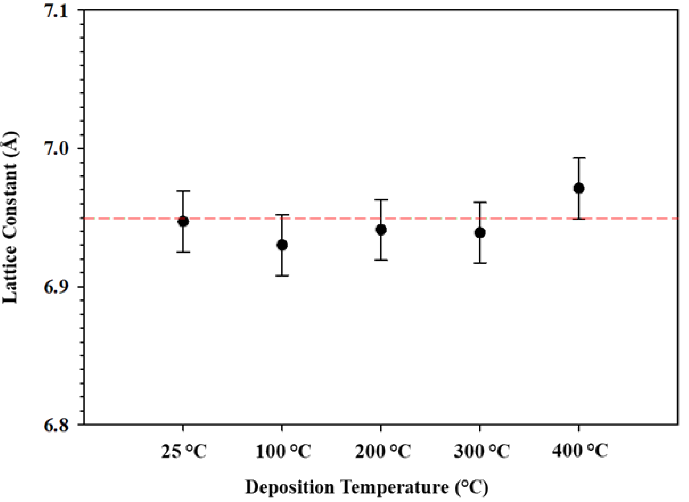
3.1. XRD Analysis
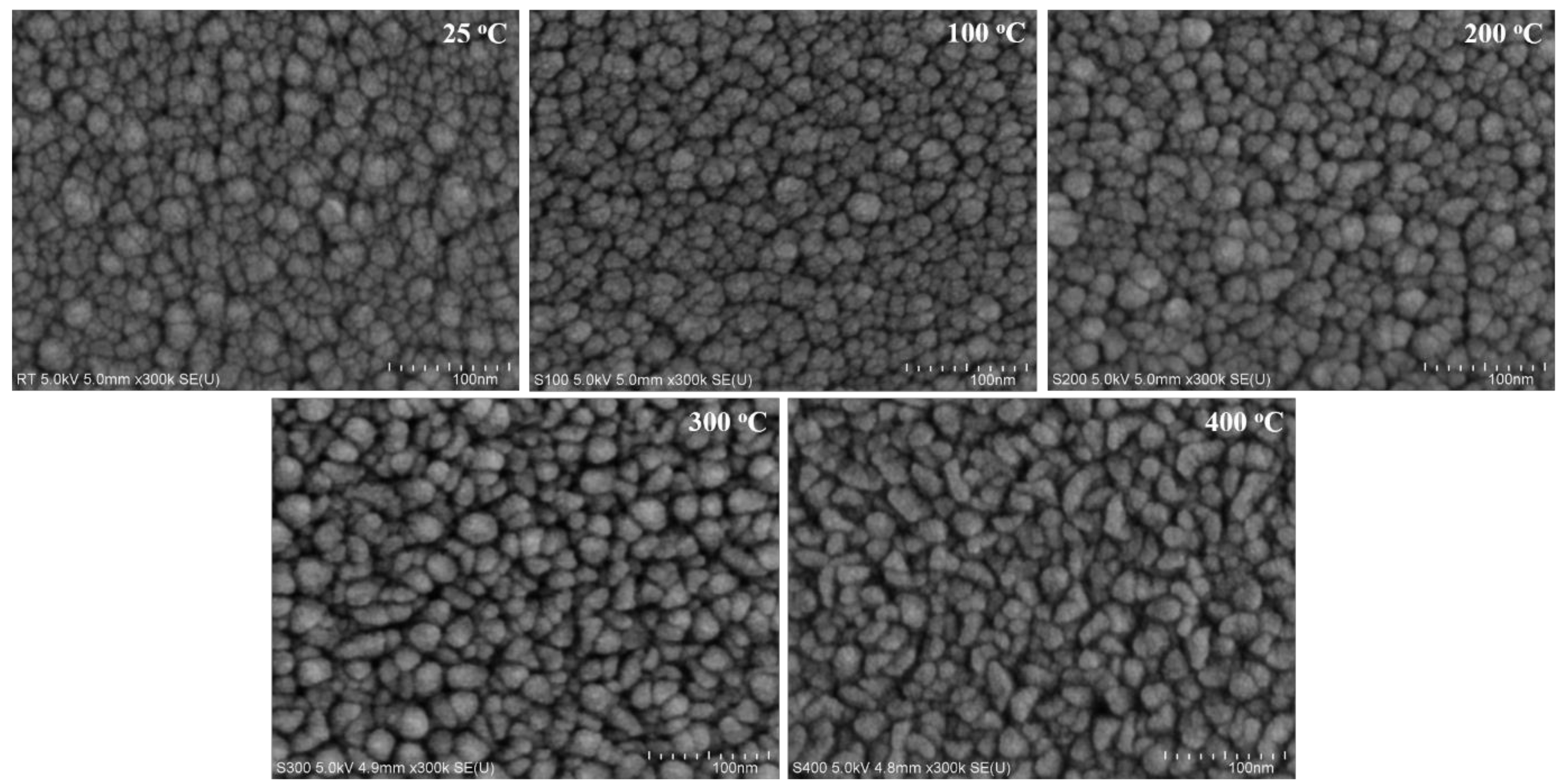
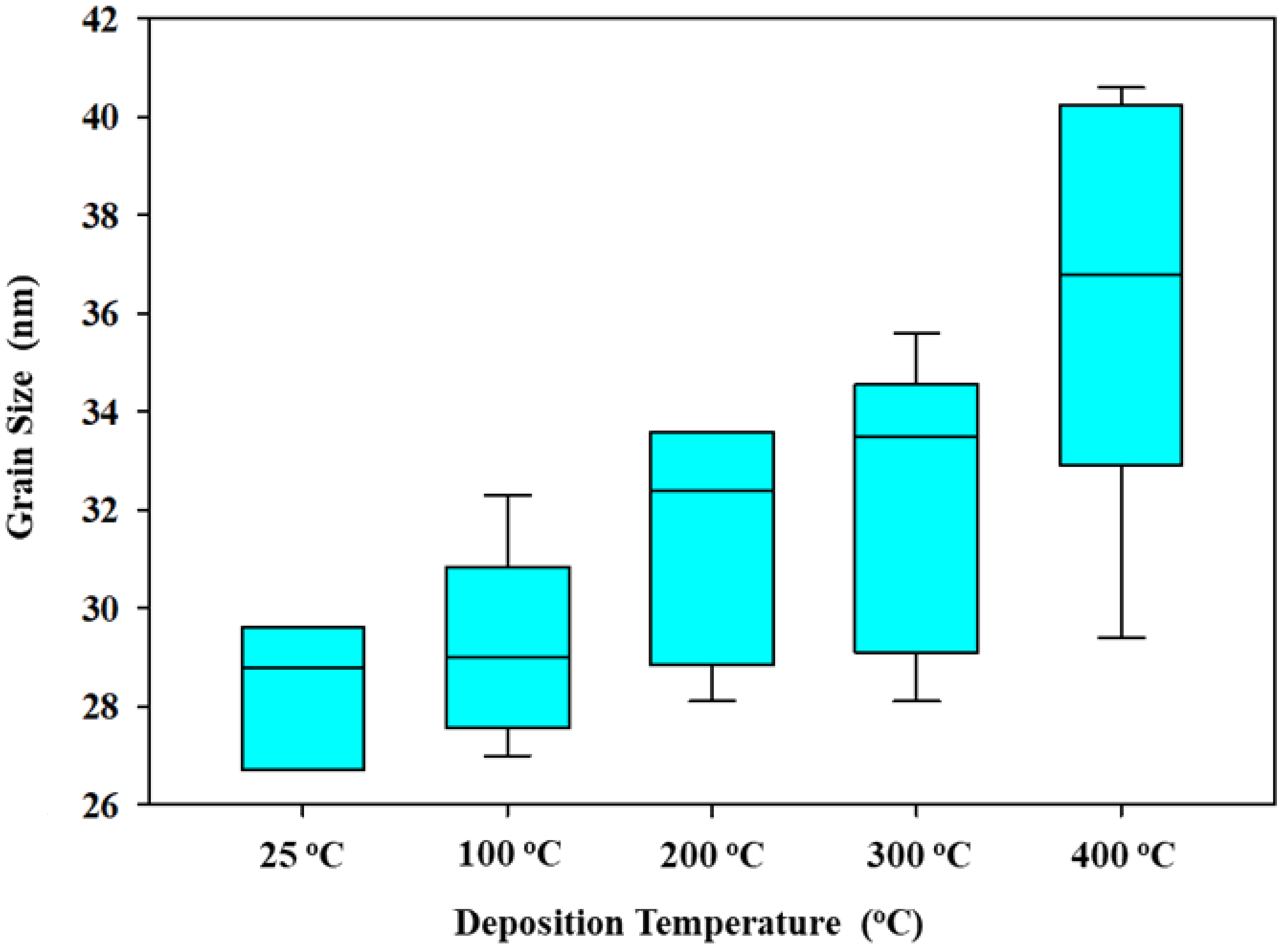
3.2. FESEM Analysis
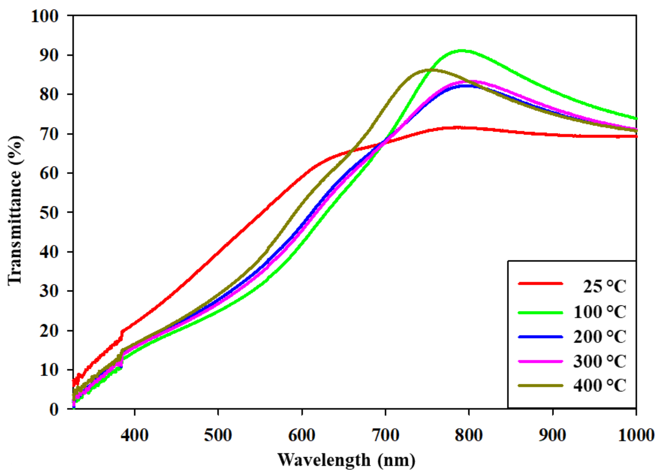
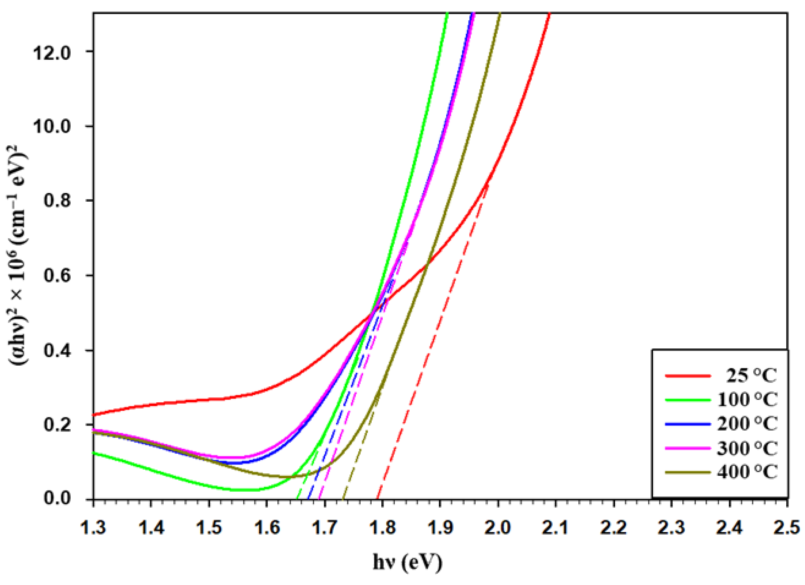
3.3. Optical Analysis
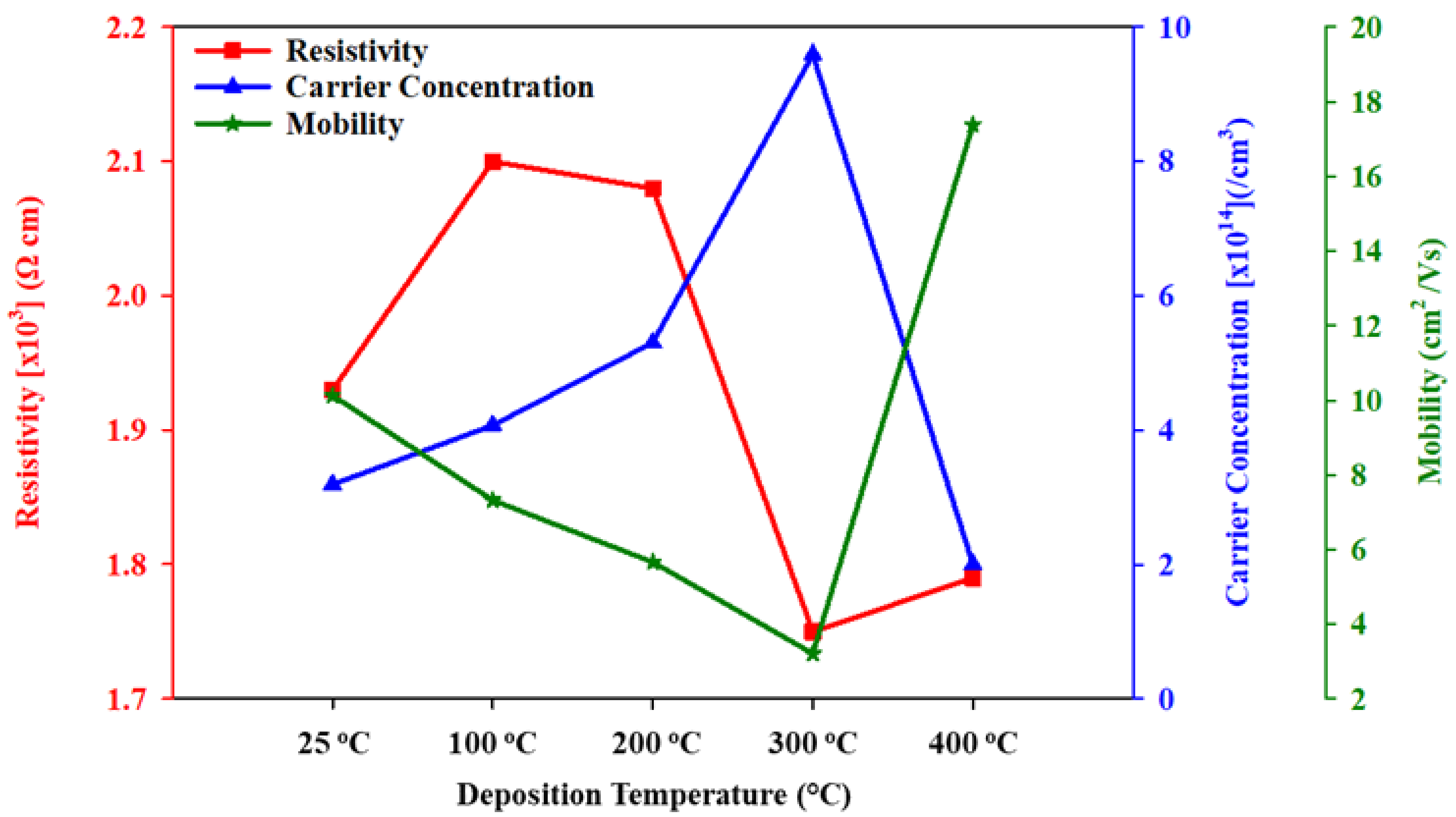
3.4. Hall Effect Measurement
4. Conclusions
Author Contributions
Funding
Institutional Review Board Statement
Informed Consent Statement
Data Availability Statement
Acknowledgments
Conflicts of Interest
References
- Gloeckler, M.; Sankin, I.; Zhao, Z. CdTe Solar Cells at the Threshold to 20% Efficiency. IEEE J. Photovolt. 2013, 3, 1389–1393. [Google Scholar] [CrossRef]
- Lai, H.; Ren, A.; Wu, L.; Hao, X.; Zhang, J.; Wang, W.; Wei, Q.; Ni, Z.; Feng, L. Laser scribing of Cd2SnO4-based CdTe polycrystalline solar cells. Renew. Energy 2020, 145, 133–140. [Google Scholar] [CrossRef]
- Salavei, A.; Menossi, D.; Piccinelli, F.; Kumar, A.; Mariotto, G.; Barbato, M.; Meneghini, M.; Meneghesso, G.; Di Mare, S.; Mariotto, G.; et al. Comparison of high efficiency flexible CdTe solar cells on different substrates at low temperature deposition. Sol. Energy 2016, 139, 13–18. [Google Scholar] [CrossRef]
- García-Alvarado, G.; De Moure-Flores, F.; Mayén-Hernández, S.; Santos-Cruz, D.; Rivera-Muñoz, E.; Contreras-Puente, G.; Pal, M.; Santos-Cruz, J. CdTe/CdS solar cells with CdTe grown at low vacuum. Vacuum 2017, 142, 175–180. [Google Scholar] [CrossRef]
- Bosio, A.; Rosa, G.; Romeo, N. Past, present and future of the thin film CdTe/CdS solar cells. Sol. Energy 2018, 175, 31–43. [Google Scholar] [CrossRef]
- Rahman, K.S.; Harif, M.N.; Rosly, H.N.; Bin Kamaruzzaman, M.I.; Akhtaruzzaman, M.; Alghoul, M.; Misran, H.; Amin, N. Influence of deposition time in CdTe thin film properties grown by Close-Spaced Sublimation (CSS) for photovoltaic application. Results Phys. 2019, 14, 102371. [Google Scholar] [CrossRef]
- Ferekides, C.; Balasubramanian, U.; Mamazza, R.; Viswanathan, V.; Zhao, H.; Morel, D. CdTe thin film solar cells: Device and technology issues. Sol. Energy 2004, 77, 823–830. [Google Scholar] [CrossRef]
- McCandless, B.E.; Dobson, K.D. Processing options for CdTe thin film solar cells. Sol. Energy 2004, 77, 839–856. [Google Scholar] [CrossRef]
- Islam, M.A.; Rahman, K.S.; Sobayel, K.; Enam, T.; Ali, A.M.; Zaman, M.; Akhtaruzzaman, M.D.; Amin, N. Fabrication of high efficiency sputtered CdS: O/CdTe thin film solar cells from window/absorber layer growth optimization in magnetron sputtering. Sol. Energy Mater. Sol. Cells 2017, 172, 384–393. [Google Scholar] [CrossRef]
- Kephart, J.; McCamy, J.; Ma, Z.; Ganjoo, A.; Alamgir, F.; Sampath, W. Band alignment of front contact layers for high-efficiency CdTe solar cells. Sol. Energy Mater. Sol. Cells 2016, 157, 266–275. [Google Scholar] [CrossRef]
- El-Menyawy, E.; Azab, A.A. Optical, electrical and photoelectrical properties of nanocrystalline cadmium selenide films for photosensor applications. Optik 2018, 168, 217–227. [Google Scholar] [CrossRef]
- Mathuri, S.; Ramamurthi, K.; Babu, R.R. Influence of deposition distance and substrate temperature on the CdSe thin films deposited by electron beam evaporation technique. Thin Solid Film. 2017, 625, 138–147. [Google Scholar] [CrossRef]
- Sahebi, R.; Roknabadi, M.R.; Behdani, M. Semi-transparent Schottky junction solar cell based on evaporated CdSe thin films: Influence of post-deposition air-annealing. Optik 2020, 204, 164204. [Google Scholar] [CrossRef]
- Li, C.; Wang, F.; Chen, Y.; Wu, L.; Zhang, J.; Li, W.; He, X.; Li, B.; Feng, L. Characterization of sputtered CdSe thin films as the window layer for CdTe solar cells. Mater. Sci. Semicond. Process. 2018, 83, 89–95. [Google Scholar] [CrossRef]
- Islam, M.A.; Rahman, K.S.; Haque, F.; Khan, N.A.; Akhtaruzzaman, M.; Alam, M.M.; Ruslan, H.; Sopian, K.; Amin, N. Effect of Sn Doping on the Properties of Nano-Structured ZnO Thin Films Deposited by Co-Sputtering Technique. J. Nanosci. Nanotechnol. 2015, 15, 9184–9191. [Google Scholar] [CrossRef]
- Poplawsky, J.D.; Guo, W.; Paudel, N.; Ng, A.; More, K.; Leonard, D.; Yan, Y. Structural and compositional dependence of the CdTex Se1−x alloy layer photoactivity in CdTe-based solar cells. Nat. Commun. 2016, 7, 12537. [Google Scholar]
- Paudel, N.R.; Yan, Y. Enhancing the photo-currents of CdTe thin-film solar cells in both short and long wavelength regions. Appl. Phys. Lett. 2014, 105, 183510. [Google Scholar] [CrossRef]
- Mia, D.; Swartz, C.H.; Paul, S.; Sohal, S.; Grice, C.R.; Yan, Y.; Holtz, M.; Li, J.V. Electrical and optical characterization of CdTe solar cells with CdS and CdSe buffers—A comparative study. J. Vac. Sci. Technol. B 2018, 36, 052904. [Google Scholar] [CrossRef]
- Lingg, M.; Spescha, A.; Haass, S.G.; Carron, R.; Buecheler, S.; Tiwari, A.N. Structural and electronic properties of CdTe1−xSex films and their application in solar cells. Sci. Technol. Adv. Mater. 2018, 19, 683–692. [Google Scholar] [CrossRef]
- Yadav, A.; Barote, M.; Masumdar, E. Studies on cadmium selenide (CdSe) thin films deposited by spray pyrolysis. Mater. Chem. Phys. 2010, 121, 53–57. [Google Scholar] [CrossRef]
- Elahi, M.; Ghobadi, N. Structural, Optical and Electrical Properties of CdSe Nanocrystalline Films. Iranian Phys. J. 2008, 2, 27–31. [Google Scholar]
- Mahato, S.; Shakti, N.; Kar, A. Annealing temperature dependent structural and optical properties of electrodeposited CdSe thin films. Mater. Sci. Semicond. Process. 2015, 39, 742–747. [Google Scholar] [CrossRef]
- Sarmah, K.; Sarma, R.; Das, H.L. Structural characterization of thermally evaporated CdSe thin films. Chalcogenide Lett. 2008, 5, 153–163. [Google Scholar]
- Wang, A.; Li, C.; Zhang, J.; Wu, L.; Wang, W.; Feng, L. Annealing temperature dependence of properties of CdSe thin films by RF-sputtering. In IOP Conference Series: Materials Science and Engineering; IOP Publishing: Bristol, UK, 2019; Volume 556, p. 012006. [Google Scholar]
- Chander, S.; Dhaka, M. Enhancement in microstructural and optoelectrical properties of thermally evaporated CdTe films for solar cells. Results Phys. 2018, 8, 1131–1135. [Google Scholar] [CrossRef]
- Kitazono, K.; Akashi, R.; Fujiwara, K.; Akita, A.; Naya, S.I.; Fujishima, M.; Tada, H. Photocatalytic Synthesis of CdS (core)–CdSe (shell) Quantum Dots with a Heteroepitaxial Junction on TiO2: Photoelectrochemical Hydrogen Generation from Water. ChemPhysChem 2017, 18, 2840–2845. [Google Scholar] [CrossRef]
- Haque, F.; Rahman, K.S.; Akhtaruzzaman; Abdullah, H.; Kiong, T.S.; Amin, N.; Tiong, S.K. Properties of sputtered ZnS thin films for photovoltaic application. Mater. Res. Express 2018, 5, 096409. [Google Scholar] [CrossRef]
- Khan, N.; Rahman, K.; Aris, K.; Ali, A.; Misran, H.; Akhtaruzzaman, M.; Tiong, S.; Amin, N. Effect of laser annealing on thermally evaporated CdTe thin films for photovoltaic absorber application. Sol. Energy 2018, 173, 1051–1057. [Google Scholar] [CrossRef]
- Harif, M.N.; Rahman, K.S.; Rosly, H.N.; Chelvanathan, P.; Doroody, C.; Misran, H.; Amin, N. An approach to alternative post-deposition treatment in CdTe thin films for solar cell application. Superlattices Microstruct. 2020, 147, 106687. [Google Scholar] [CrossRef]
- Rosly, H.N.; Rahman, K.S.; Harif, M.N.; Doroody, C.; Isah, M.; Misran, H.; Amin, N. Annealing temperature assisted microstructural and optoelectrical properties of CdSe thin film grown by RF magnetron sputtering. Superlattices Microstruct. 2020, 148, 106716. [Google Scholar] [CrossRef]
- Murali, K.; Sivaramamoorthy, K.; Kottaisamy, M.; Bahadur, S.A. Photoconductive studies on electron beam evaporated CdSe films. Phys. B Condens. Matter 2009, 404, 2449–2454. [Google Scholar] [CrossRef]
- Patel, S.; Purohit, A.; Chander, S.; Kannan, M.; Dhaka, M. An approach to MgCl2 activation on CdSe thin films for solar cells. Curr. Appl. Phys. 2018, 18, 803–809. [Google Scholar] [CrossRef]
- Göde, F.; Ünlü, S. Synthesis and characterization of CdS window layers for PbS thin film solar cells. Mater. Sci. Semicond. Process. 2019, 90, 92–100. [Google Scholar] [CrossRef]
- Islam, M.A.; Rahman, K.S.; Haque, F.; Dhar, N.; Salim, M.; Akhtaruzzaman, M.; Sopian, K.; Amin, N. Opto-electrical properties of in doped CdS thin films by co-sputtering technique. J. Ovonic Res. 2014, 10, 185–190. [Google Scholar]
- Gorji, N.E. Oxygen incorporation into CdS/CdTe thin film solar cells. Opt. Quantum Electron. 2015, 47, 2445–2453. [Google Scholar] [CrossRef]
- Khomchenko, A.V.E. Waveguide Spectroscopy of Thin Films; Elsevier: Amsterdam, The Netherlands, 2005. [Google Scholar]
- Mendoza, M.F.; Pérez, R.C.; Torres-Delgado, G.; Marín, J.M.; Orea, A.C.; Zelaya-Angel, O. Structural, morphological, optical and electrical properties of CdTe films deposited by CSS under an argon–oxygen mixture and vacuum. Sol. Energy Mater. Sol. Cells 2011, 95, 2023–2027. [Google Scholar] [CrossRef]
- Akbarnejad, E.; Ghorannevis, Z.; Abbasi, F.; Ghoranneviss, M. Investigation of annealing temperature effect on magnetron sputtered cadmium sulfide thin film properties. J. Appl. Phys. 2016, 11, 45–49. [Google Scholar] [CrossRef]
- Das, N.; Chakrabartty, J.; Farhad, S.; Gupta, A.S.; Ahamed, E.I.; Rahman, K.; Wafi, A.; Alkahtani, A.; Matin, M.; Amin, N. Effect of substrate temperature on the properties of RF sputtered CdS thin films for solar cell applications. Results Phys. 2020, 17, 103132. [Google Scholar] [CrossRef]


| Device Structure | Efficiency [%] | FF [%] | Voc [mV] | Jsc [mA/cm2] | Source |
|---|---|---|---|---|---|
| CdSe (100 nm, RFMS)/ CdTe(CSS) | 12.6 | 60.2 | 770 | 27 | Poplawsky et al. [16] |
| CdS (100 nm, RFMS)/ CdTe(CSS) | 14.5 | 75.4 | 810 | 23.8 | |
| CdSe (100 nm, RFMS)/ CdTe (CSS) | 12.1 | 64.8 | 690 | 26.9 | Mia et al. [18] |
| CdS (140 nm, RFMS)/ CdTe (CSS) | 14.6 | 70 | 847 | 24.7 | |
| CdSe (100 nm, RFMS)/ CdTe (CSS) | 14.7 | 69.4 | 771 | 27.5 | Paudel and Yan [17] |
| CdS (15 nm, RFMS)/ CdSe (100 nm, RFMS)/ CdTe (CSS) | 14.1 | 64.1 | 806 | 27.2 | |
| CdS (130 nm, RFMS)/ CdTe (CSS) | 14.8 | 75.5 | 811 | 24.2 | |
| CdS (30 nm, HVE)/ CdSe (60 nm, HVE)/ CdTe (HVE) | 12.2 | 67 | 710 | 25.6 | Lingg et al. [19] |
| CdS (120 nm, HVE)/ CdTe (HVE) | 10.5 | 69.4 | 830 | 18.5 |
| Parameter | Condition |
|---|---|
| RF power | 40 watts |
| Ar gas flow | 5 SCCM |
| Deposition time | 15 min |
| Base pressure | 1.5 × 10⁻⁵ Torr |
| Deposition pressure | 2.0 × 10⁻² Torr |
| Deposition temperature | 25 °C, 100 °C, 200 °C, 300 °C, 400 °C |
| Deposition Temperature | hkl | C (Å) | Dhkl (nm) | D (nm) | ε [×10−3] | δ [×1011] (cm−2) |
|---|---|---|---|---|---|---|
| 25 °C | (002) | 6.947 | 0.3474 | 33.964 | 4.602 | 0.867 |
| 100 °C | (002) | 6.922 | 0.3461 | 33.970 | 4.585 | 0.867 |
| 200 °C | (002) | 6.941 | 0.3469 | 36.391 | 4.291 | 0.755 |
| 300 °C | (002) | 6.939 | 0.3470 | 38.818 | 4.022 | 0.664 |
| 400 °C | (002) | 6.988 | 0.3494 | 31.831 | 4.940 | 0.987 |
| Deposition Temperature | Energy Band Gap (Eg) |
|---|---|
| 25 °C | 1.79 |
| 100 °C | 1.65 |
| 200 °C | 1.67 |
| 300 °C | 1.69 |
| 400 °C | 1.73 |
| Deposition Temperature | Carrier Concentration (/cm3) | Mobility (cm2/Vs) | Resistivity [×103] (Ω cm) | Semiconductor Type |
|---|---|---|---|---|
| 25 °C | 3.19 × 10¹⁴ | 10.13 | 1.93 | n-type |
| 100 °C | 4.07 × 10¹⁴ | 7.32 | 2.10 | n-type |
| 200 °C | 5.30 × 10¹⁴ | 5.66 | 2.08 | n-type |
| 300 °C | 9.59 × 10¹⁴ | 3.21 | 1.75 | n-type |
| 400 °C | 2.00 × 10¹⁴ | 17.38 | 1.79 | n-type |
Publisher’s Note: MDPI stays neutral with regard to jurisdictional claims in published maps and institutional affiliations. |
© 2021 by the authors. Licensee MDPI, Basel, Switzerland. This article is an open access article distributed under the terms and conditions of the Creative Commons Attribution (CC BY) license (http://creativecommons.org/licenses/by/4.0/).
Share and Cite
Rosly, H.N.; Rahman, K.S.; Abdullah, S.F.; Harif, M.N.; Doroody, C.; Chelvanathan, P.; Misran, H.; Sopian, K.; Amin, N. The Role of Deposition Temperature in the Photovoltaic Properties of RF-Sputtered CdSe Thin Films. Crystals 2021, 11, 73. https://doi.org/10.3390/cryst11010073
Rosly HN, Rahman KS, Abdullah SF, Harif MN, Doroody C, Chelvanathan P, Misran H, Sopian K, Amin N. The Role of Deposition Temperature in the Photovoltaic Properties of RF-Sputtered CdSe Thin Films. Crystals. 2021; 11(1):73. https://doi.org/10.3390/cryst11010073
Chicago/Turabian StyleRosly, Hasrul Nisham, Kazi Sajedur Rahman, Siti Fazlili Abdullah, Muhammad Najib Harif, Camellia Doroody, Puvaneswaran Chelvanathan, Halina Misran, Kamaruzzaman Sopian, and Nowshad Amin. 2021. "The Role of Deposition Temperature in the Photovoltaic Properties of RF-Sputtered CdSe Thin Films" Crystals 11, no. 1: 73. https://doi.org/10.3390/cryst11010073
APA StyleRosly, H. N., Rahman, K. S., Abdullah, S. F., Harif, M. N., Doroody, C., Chelvanathan, P., Misran, H., Sopian, K., & Amin, N. (2021). The Role of Deposition Temperature in the Photovoltaic Properties of RF-Sputtered CdSe Thin Films. Crystals, 11(1), 73. https://doi.org/10.3390/cryst11010073