Abstract
The surface defect detection of printed circuit boards (PCBs) plays a crucial role in the field of industrial manufacturing. However, the existing PCB defect detection methods have great challenges in detecting the accuracy of tiny defects under the complex background due to its compact layout. To address this problem, we propose a novel YOLO-AMBA-EASPP-BiFPN (YOLO-AEB) network based on the YOLOv10 framework that achieves high precision and real-time detection of tiny defects through multi-level architecture optimization. In the backbone network, an adaptive multi-branch attention mechanism (AMBA) is first proposed, which employs an adaptive reweighting algorithm (ARA) to dynamically optimize fusion weights within the multi-branch attention mechanism (MBA), thereby optimizing the ability to represent tiny defects under complex background noise. Then, an efficient atrous spatial pyramid pooling (EASPP) is constructed, which fuses AMBA and atrous spatial pyramid pooling-fast (ASPF). This integration effectively mitigates feature degradation while preserving expansive receptive fields, and the extraction of defect detail features is strengthened. In the neck network, the bidirectional feature pyramid network (BiFPN) is used to replace the conventional path aggregation network (PAN), and the bidirectional cross-scale feature fusion mechanism is used to improve the transfer ability of shallow detail features to deep networks. Comprehensive experimental evaluations demonstrate that our proposed network achieves state-of-the-art performance, whose F1 score can reach 95.7% and mean average precision (mAP) can reach 97%, representing respective improvements of 7.1% and 5.8% over the baseline YOLOv10 model. Feature visualization analysis further verifies the effectiveness and feasibility of YOLO-AEB.
1. Introduction
Surface defect detection of PCB is a crucial step to ensure the reliability and stability of electronic devices [1]. Existing PCB defect detection methodologies have evolved through three primary development stages: traditional image processing (e.g., edge detection [2], Fourier transformation [3]), machine learning (e.g., support vector machine [4]), and deep learning-based methods (e.g., convolutional neural networks [5]). Among them, deep learning-based methods have become the predominant research hotspot in the field of industrial defect detection due to their superior feature representation capabilities.
Deep learning-based detection networks are primarily categorized into two-stage networks and one-stage networks. Two-stage networks (e.g., Faster R-CNN [6], Mask R-CNN [7]) adopt the principle of candidate box generation first, and target recognition later, which has the defects of high computational complexity and large inference delay. In contrast, one-stage networks (e.g., single shot detector [8], you only look once (YOLO) series [9]) achieve real-time detection through the anchor box or by directly using the network, which is more suitable for industrial real-time detection scenarios with its significant speed advantage.
In recent years, researchers have proposed a variety of improvement schemes according to the shortcomings of two-stage networks and one-stage networks: In two-stage networks, Fan et al. [10] proposed an improved Faster R-CNN network to detect solder joint defects and PCB components. Lian et al. [11] added the geometric attention guided mask branch to the R-CNN model to improve the detection accuracy. In one-stage networks, Chaudhari et al. [12] improved the YOLOv3 model and used multi-scale operation enhancement to detect PCB defects of different sizes. Ye et al. [13] improved the YOLOv5 to realize the defect detection of PCB. Despite the above research and improvements achieving great results in PCB defect detection, there are still the following problems in the face of complex industrial scenarios:
- Tiny defect detection limitations: With the improvement of PCB routing accuracy, the defect size is generally reduced to 0.1–0.5 mm2, which leads to the lack of feature representation ability of the network.
- Background interference susceptibility: defect-like texture noise generated by high-density wiring seriously reduces the feature discrimination of the model.
To address the aforementioned challenges, we propose an enhanced PCB defect detection framework named YOLO-AEB. While the individual components draw inspiration from existing concepts, the principal novelty of our work lies in their co-adaptive design and deep specialization within the YOLOv10 framework to form a holistic solution for PCB defect detection. This integrated architecture specifically addresses the intertwined problems of tiny defect size and complex background noise, which are not adequately solved by simply plugging in existing modules. The main innovations are as follows:
- A YOLO-AEB network based on improved YOLOv10 is proposed to achieve high-precision detection of tiny defects while ensuring the real-time requirements of industrial defect detection are met.
- The Adaptive Multi-branch Attention (AMBA) mechanism is innovatively designed. Unlike existing single-branch (e.g., ECA-Net [14]) or sequentially fused attention mechanisms (e.g., CBAM), AMBA employs parallel branches to extract channel, width, and context features simultaneously. Crucially, it introduces an Adaptive Reweighting Algorithm (ARA) to dynamically adjust the fusion weights of these branches based on the input defect type, overcoming the limitations of static, one-size-fits-all attention allocation.
- A novel Efficient Atrous Spatial Pyramid Pooling (EASPP) module is developed. EASPP represents the first integration of our proposed AMBA with hybrid dilated convolutions. This co-design not only expands the receptive field to mitigate feature loss but also incorporates defect-aware feature recalibration, enabling more precise multi-scale feature extraction compared to standard modules.
- The BiFPN structure is used for feature information fusion, and the bidirectional cross-scale feature fusion mechanism is used to improve the transmission ability of shallow detail features to deep networks.
2. Related Works
2.1. YOLO-Based Methods of PCB Defect Detection
Since their inception, the YOLO models have undergone continuous iterations and achieved remarkable success in the field of object detection. They have progressively evolved into standardized architecture consisting of three key components: a backbone network for feature extraction, a neck network for feature fusion, and a detection head for prediction output. Within PCB defect detection specifically, researchers have adapted YOLO variants to meet industrial requirements. Wang et al. [15] combined the BiFPN structure with the YOLOv5 model to detect PCB defects. Benchen et al. [16] proposed a PCB defect detection network combining the REPVGG structure and Yolov7-Tiny to enhance the accuracy of the model. Liu et al. [17] proposed a MobileViT-YOLO model combining a new multi-scale feature fusion structure and a decoupled head structure to detect PCB defects. Hua et al. [18] used a lightweight backbone network and a new loss function in the YOLOv7-Tiny to reduce the inference speed and improve the detection accuracy of defects. Lan et al. [19] proposed a PCB defect detection model based on improved YOLOv8 and added a cross-scale fusion module (CFM) to improve the model detection performance. Hu et al. [20] introduced the Hierarchical Attention with Transformer (HAT) mechanism into YOLOv8 to improve the detection ability of defects. However, the accuracy of these improved methods for defect detection decreases when facing the influence of tiny defect sizes and noise caused by high-density wiring. Selvam et al. [21] found that by improving YOLOv11 and incorporating the Swin Transformer and CMBA attention mechanism, the detection accuracy for multi-scale defects can be enhanced. Yin et al. [22] utilized the median enhancement channel and the spatial attention mechanism to improve YOLOv12, in order to enhance the features of PCB defects. Wu et al. [23] proposed the YOLO Efficient Multi-scale Adaptive Channel (YOLO-EMAC) framework, based on the enhanced YOLOv12 architecture, aiming to improve the accuracy, efficiency, and generalization of small defect detection.
While subsequent iterations like YOLOv11 and YOLOv12 have introduced advanced designs such as multi-kernel convolution and region-specific attention mechanisms, their inherent architectural pathways would intertwine with and confound the evaluation of our core contributions: the AMBA mechanism and EASPP module. To ensure a clear and isolated assessment of our proposed components, we base our model on YOLOv10, which provides a powerful yet structurally neutral foundation that allows for the direct and unambiguous validation of their effectiveness in PCB defect detection. YOLOv10 [24] addresses performance limitations through three key architectural innovations: Firstly, the introduction of compact inverted blocks (CIB), which solved the problem that previous versions were prone to exhibiting more redundancy in the depth stage and large model, and the depthwise separable convolution [25] is used to realize space-channel mixing. Secondly, the progressive self-attention (PSA) module includes the multi-head self-attention (MHSA) [26] and feed-forward networks (FFN) [27] to improve the ability of fine-grained feature capture. Finally, YOLOv10 uses consistent dual assignment without non-maximum suppression (NMS) [28] training and dual label assignment at the detection head. The one-to-one matching (inference stage) assigns only one prediction to each true label, thus avoiding NMS post-processing. At the same time, one-to-many matching (training stage) enriches the supervision signal by assigning multiple positive samples to each instance.
The industrial defect detection efficacy of YOLOv10 has been extensively validated: Mao et al. [29] applied the YOLOv10 model to submillimeter fabric tear detection and achieved great results. Haoyan et al. [30] designed an improved lightweight EAD-YOLOv10 model, which improved the model’s ability to detect steel surface defects by using an adaptive downsampling layer. Ali et al. [31] combined the improved visual transformer (ViT) with YOLOv10 to detect and classify concrete cracks. Mei et al. [32] proposed a lightweight BGF-YOLOv10 model to detect tiny targets by improving the backbone network and neck network of the YOLOv10. Liao et al. [33] proposed an innovative detection system, YOLOv10nSFDC, which adopted advanced elements such as the Dual Convolution (DConv) to improve the model’s ability to detect steel surface defects. These results verify significant advantages of YOLOv10 in tiny defect detection and provide a theoretical basis for this study.
2.2. Attention Mechanism
The increasing complexity of PCB component layouts intensifies background interference and noise contamination, significantly impairing model capabilities in tiny defect identification (typically < 0.5 mm2). The attention mechanism [34] can assign a higher weight to the defect part and reduce the weight of the background noise, thereby enhancing the defect feature information and effectively suppressing the noise interference.
Many researchers have introduced the attention mechanism into the model and achieved notable performance gains. Qin et al. [35] added the Gather-and-Distribute mechanism to the YOLOv5 backbone network to strengthen the fusion of deep semantic information and shallow semantic information to complete the detection. Yuan et al. [36] proposed a YOLO-HMC network, which combined the improved multi-convolutional attention module with YOLOv5 to highlight the defect location and improve model detection accuracy. Huang et al. [37] proposed the neighborhood correlation enhanced network to effectively use the defect and surrounding relationship information and accurately distinguish the authenticity of the defect. Yue et al. [38] introduced the SE mechanism into the YOLOv7 network to enhance the ability to extract defect features and improve the accuracy of model detection. Bai et al. [39] integrated the efficient attention mechanism (ECA) into the backbone network of YOLOv8 to improve the detection performance of tiny target defects by adaptively enhancing the expressiveness of key features. These methods adopt a single branch and static weight allocation strategy, which is difficult to dynamically adapt to complex industrial scenarios.
3. Methodology
3.1. Overall Framework of YOLO-AEB
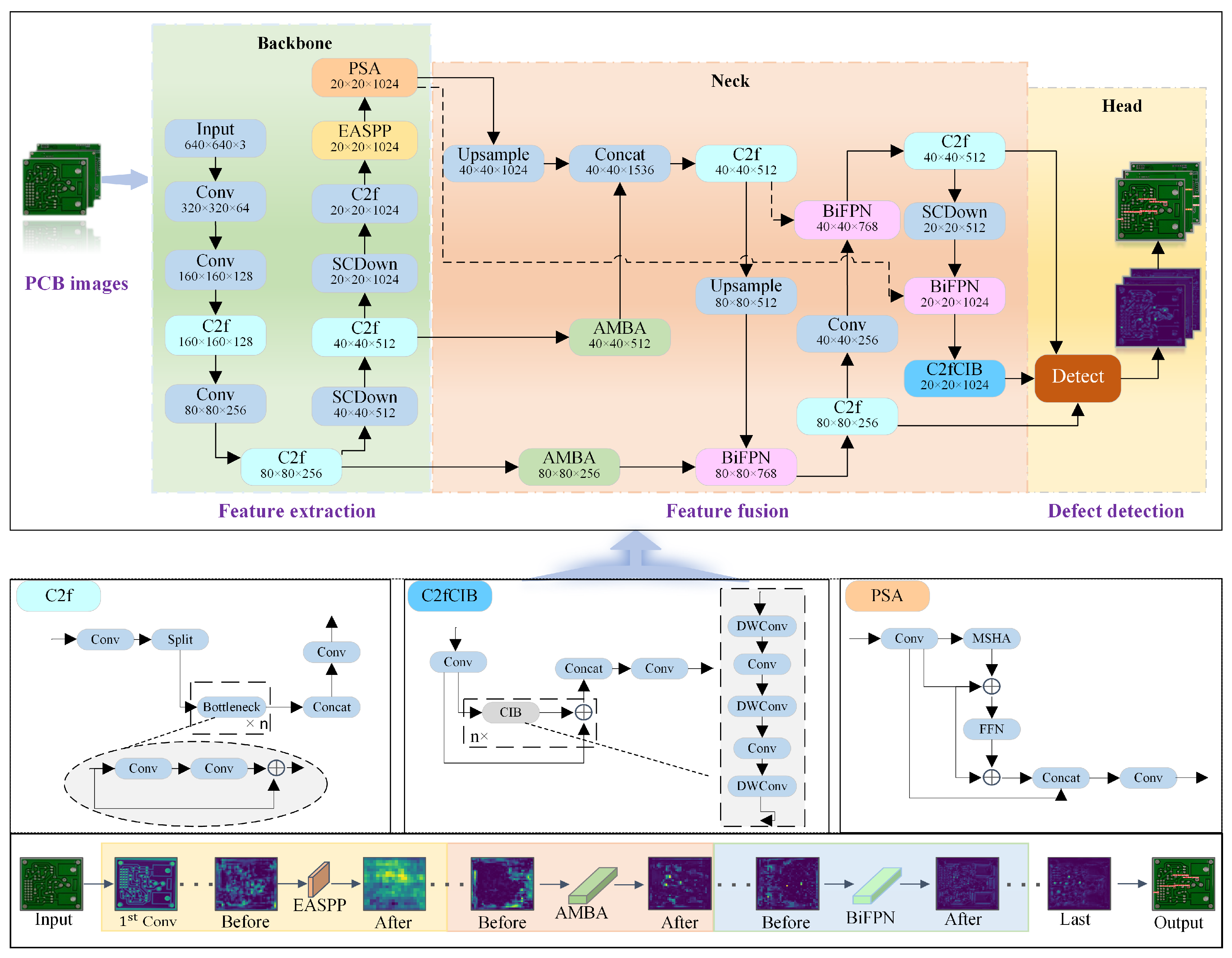
As shown in Figure 1, we propose a YOLO-AEB network model based on improved YOLOv10, which consists of the backbone network for feature extraction, the neck network for feature fusion, and the detection head for the output of the result.
Figure 1.
Framework of YOLO-AEB.
The optimized backbone incorporates two key innovative components that work in concert:
On one hand, the AMBA module is embedded into the backbone. In contrast to the Efficient Channel Attention (ECA) module used in the MBAM, which only performs channel-wise re-calibration, our AMBA processes features across three complementary dimensions (channel, width, context) and adaptively fuses them. This allows the model to dynamically prioritize the most relevant feature dimension for different defect types (e.g., channel for point defects, width for linear defects), significantly enhancing feature representation under complex background noise.
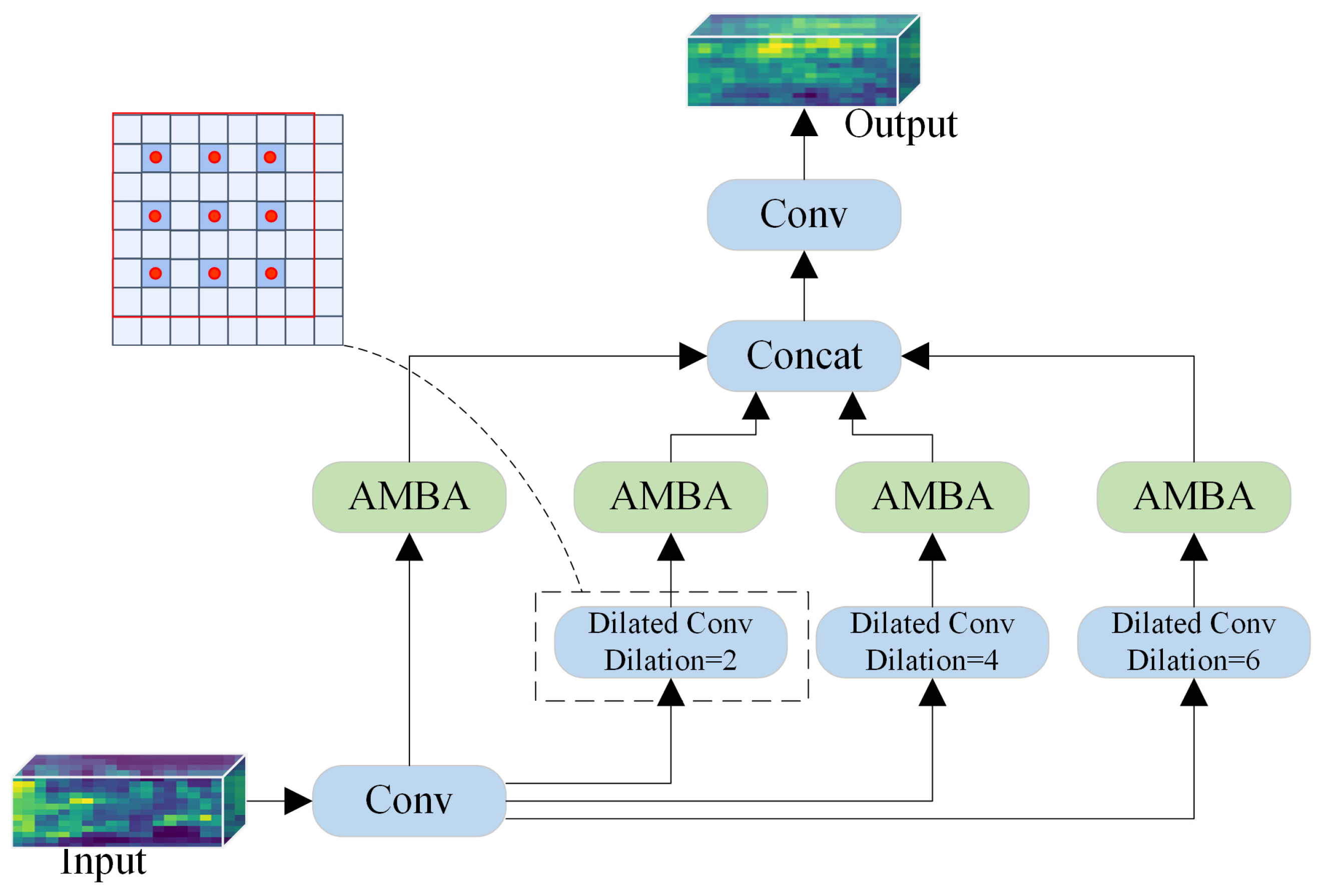
On the other hand, we construct the EASPP module to replace the standard SPPF. While the original SPPF uses fixed max-pooling kernels and Atrous Spatial Pyramid Pooling-Fast (ASPF) [40] simply replaces them with dilated convolutions, our EASPP goes a step further by integrating the AMBA mechanism after each parallel dilated convolution branch. This integration is pivotal: the dilated convolutions preserve a large receptive field [41] and prevent detail loss, while the subsequent AMBA adaptively suppresses background noise and highlights defect-specific features within each receptive field, strengthening the extraction of multi-scale defect details.
In the neck network, to address the problem that the traditional Path Aggregation Network (PAN) [42] uses equal-weight fusion which diminishes the contribution of tiny defect features, we adopt the BiFPN structure [43]. Compared with PAN, BiFPN not only simplifies the topology by removing nodes with minor contributions but also introduces a learnable weighted fusion mechanism. This ensures that rich shallow detail features are effectively transferred and fused with deep semantic features, thereby improving the detection capability for tiny defects.
3.2. Description of the Improvements
3.2.1. Adaptive Muti-Branch Attention (AMBA)
In the PCB defect detection process, there are a large number of defects and similar background noise features, which will make the network unable to distinguish defects from background information, greatly increasing the difficulty of extracting defect features. To address this, the present study incorporates the AMBA into the backbone layer to enhance the attention toward critical regions. As illustrated in Figure 2, this module mainly consists of two parts: the first part utilizes MBA to generate three attention branches, and the second part employs ARA to dynamically adjust the three generated attention branches.
Figure 2.
Diagram of AMBA structure.
It is worth noting that MBA mainly deals with the features of the three dimensions of channel, width, and context to improve the discrimination between defects and background features of the model. As shown in Figure 2, MBA will divide the input image into three branches: , , and , where H, W, and C denote the height, width, and number of channels of the input feature map x. The relevant calculation is shown in Equation (1). Second, the channel dimension compresses the spatial dimension of the input feature map by multilayer perceptron and normalizes it to generate the channel attention map . The width and context dimensions are then processed by standard convolution and normalization to generate corresponding channel attention maps (i = 2, 3). Then, the attention weight is multiplied with the corresponding original feature map to generate new feature maps . Finally, the feature maps of width and context dimensions are converted into RC × H × W states, and the relevant calculation is shown in Equations (2) and (3).
where represents the state of the transition feature map, represents multilayer perceptron, represents the global average pooling, represents the global max pooling, represents the convolutional layer, σ represents the sigmoid activation function, and represents concatenation operation.
As shown in Figure 3, different types of defects have different degrees of dependence on the three dimensions. Point defects such as missing hole, mouse bite, and spur are more dependent on channel branches; linear defects such as open circuit, short circuit, and spurious copper are more dependent on the width branch; and the weight of the context branch is more dependent on the defects in the complex environment of the high-density wiring area, and directly using the average weighting will lead to performance degradation of the model. Therefore, we propose to use ARA to adaptively weight the three branches generated by MBA and assign different weighting coefficients according to the needs of different types of defects.
Figure 3.
Heat map of weight distribution (α, β, and γ distribution for different defect types).
The proposed ARA realizes the dynamic fusion of multi-branch attention through a differentiable weight learner, and its core idea is to automatically learn the importance weights of different dimensional features through an end-to-end. Specifically, the output features of the three branches of MBA were concatenated along the channel dimension, and compressed into a channel description vector by global average pooling (GAP), retaining the corresponding strength of global features of each branch; related calculations are given in (4). Secondly, the weight generation network is designed to dynamically assign branch weights through the learnable parameters. The learned optimal weight coefficients α, β, and γ correspond to the attention branch weights of three dimensions of channel, width, and context, respectively, and satisfy α + β + γ = 1. The relevant calculation is shown in (5). Finally, the weight coefficient is weighted and fused with each branch to obtain the final result.
where and represent the learnable parameter matrices ( is the hidden dimension), and represents the Relu activation function.
3.2.2. Efficient Atrous Spatial Pyramid Pooling (EASPP)
Traditional max pooling [44] tends to filter out detail information characterized by low surrounding pixel values, resulting in the loss of local detail information pertaining to tiny defects. The limitation is particularly evident when applying max pooling through SPPF [45] to defect features, as shown in Figure 4b. To address this critical issue, we draw on the ideal of ASPF that introduces dilated convolution to inject holes into the convolution kernel to expand the receptive field, generating feature maps with varying receptive fields via the utilization of different dilation rates to solve the problem of feature loss. However, the ECA employed by the ASPF only enhances the defect features at the channel level; the proposed AMBA can process the defect features from three dimensions and adaptively weight them according to the types of defects, which enhances the ability to extract defect features to a certain extent, as illustrated in Figure 4c. Therefore, AMBA is introduced to replace ECA to co-design a new module, EASPP, which not only solves the problem of feature loss, but also enhances the branch of effective receptive field according to the type of defect.
Figure 4.
Comparison of feature information of different pooling modules. (a) Input, (b) SPPF, (c) EASPF.
As shown in Figure 5, the EASPP module employs a three-layer architecture, and the first layer applies a standard convolution that processes the input feature map x from the preceding layers, yielding foundational features . In the second layer, four parallel processing pathways are input to the basic feature map for multi-branch expansion. One pathway is directly processed by AMBA to obtain the feature map of the original receptive field, and the other three pathways use dilated convolution with different dilation rates (rates = 2, 4, 6) to obtain the feature maps , , and after expanding the receptive field, and then the obtained feature maps are processed by AMBA, generating enhanced feature maps (i = 2, 3, 4). The third layer concatenates the enhanced feature maps generated and uses 1 × 1 convolution for channel dimension reduction to obtain the final result.
Figure 5.
Diagram of EASPP structure.
Assuming that input , the EASPP process can be expressed as the following equations:
where represents the dilated convolution, R represents the dilation rate.
3.2.3. Bidirectional Feature Pyramid Network (BiFPN)
When the PAN performs feature fusion, the equal-weight feature fusion strategy reduces the feature contribution of tiny defects. Therefore, BiFPN is adopted in this paper to enhance the feature fusion ability of the model through architecture optimization and weighted fusion mechanism.
As shown in Figure 6a, architecture optimization improves the transfer ability of shallow detail features to deep networks by removing one-sided input nodes and adding cross-layer direct connections. Taking layers 6 and 7 as an example, the intermediate node of layer 7 is deleted and a hop connection path is added between the input and output of layer 6. Weighted fusion improves the contribution of tiny defect features in the feature map by assigning learnable weights to input features. Taking layer 6 as an example, the intermediate nodes are calculated as Equation (10) and the output nodes are calculated as Equation (11). To amplify the fusion efficacy, BiFPN considers each bidirectional path as a feature network layer and repeats the layer many times (three times in this paper), as shown in Figure 6b.
where represents the output node, represents the input node, represents the intermediate node, represents the upsampling, represents the learning parameter, and represents the learning rate.
Figure 6.
Diagram of BiFPN structure. (a) BiFPN, (b) BiFPN Layer.
4. Experiments and Results
4.1. Design of Experiments
4.1.1. Experimental Environment
The hardware in the experiments used the Windows 11 operating system with an Intel Core i5-13400 CPU, 16 GB memory, and an NVIDIA GeForce RTX4060 with 8 GB video memory. The software environment is based on the Pytorch 2.2.2 framework with the CUDA 11.8 acceleration library, Python version 3.8.3. In the experiment, the number of epochs is set to 300, the initial learning rate is set to 0.01, the size of input image is set to 640 × 640, and the batch size is 8.
4.1.2. Datasets
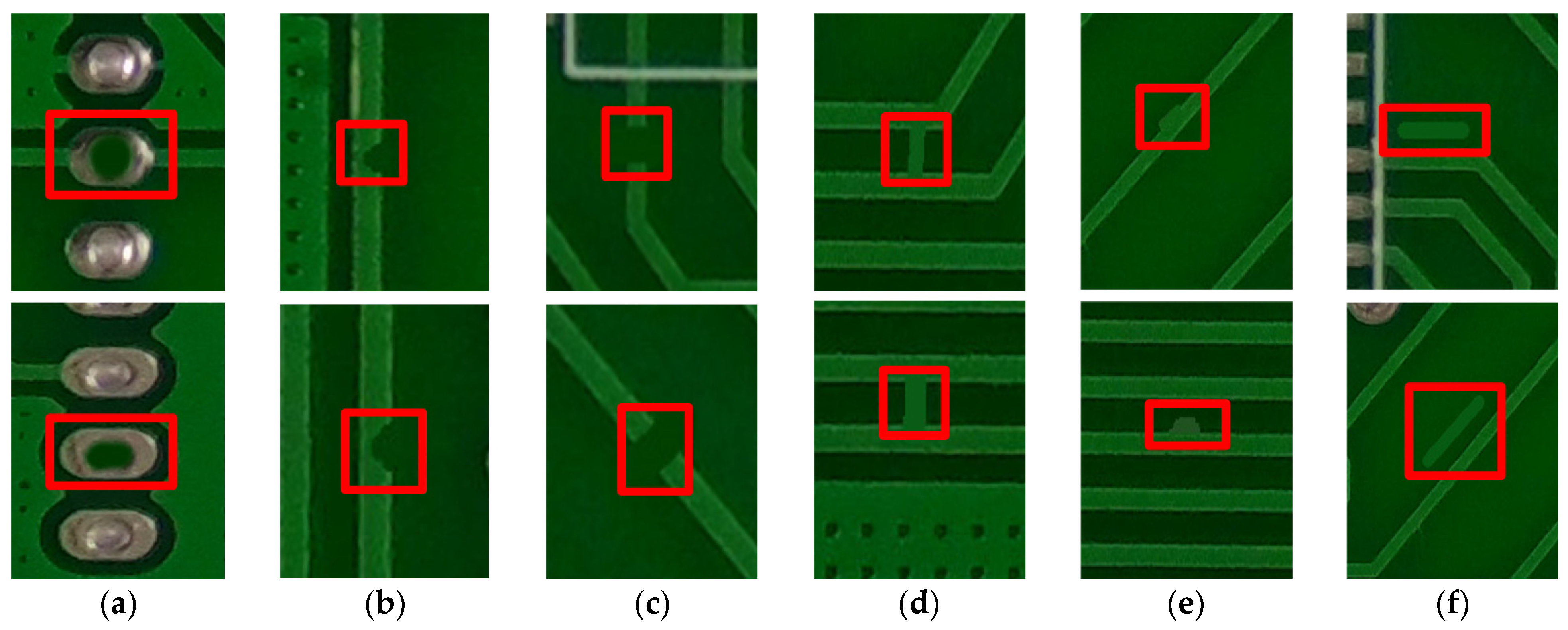
As shown in Figure 7, the dataset used in the experiment is the public dataset HRIPCB [46] released by Peking University, which includes 693 PCB images covering six types of defects, and each image includes 3 to 5 defects. To increase the generalization performance of the model, we expand the dataset by traditional image processing operations (such as translation of image size, mirroring, adding Gaussian noise (σ = 0.01), rotating degrees, etc.), and finally expand the sample size to 4158 to enhance the robustness and generalization ability of the model. The division ratio of the training set and the test set in this experiment is 8:2.
Figure 7.
Dataset defect diagram: (a) missing hole; (b) mouse bite; (c) open circuit; (d) short circuit; (e) spur; (f) spurious copper.
4.1.3. Evaluation Indicators
In the field of defect detection, model evaluation indicators include , , , and . refers to the proportion of the samples of correctly detected as positive in all samples predicted as positive. refers to the proportion of the samples of correctly identified as positive in all actual positive samples. However, the two indicators often interact with each other. When is higher, it often leads to reduced , and vice versa. To comprehensively evaluate the performance of the model with these two indicators, is commonly employed for evaluation. The is obtained by averaging the AP of different types and is a common comprehensive performance metric in object detection tasks.
The calculation formulas of , , , and are expressed as follows:
where represents the true positives, represents the false positives, false negatives, and represents the total number of defect classes.
4.2. Comparative Experimental
Conducted under the specified experimental conditions and utilizing the HRIPCB dataset, the training results are shown in Figure 8. It can be observed from the results that the loss values of each item exhibit a precipitous decline during the initial 100 epochs. Precision, recall, and indicators demonstrate progressive stabilization through coordinated parameter refinement, and ultimately tend to converge between 100 and 300 epochs.
Figure 8.
Diagram of model training results. (a–d) Loss change curve during training, (e) precision of the model, (f) recall of the model, (g) mAP of the model.
It can be seen from Table 1 that the proposed YOLO-AEB network achieves superior detection accuracy across all defect types, achieving an overall of 95.7% and of 97%. Particularly noteworthy is its performance on large defects such as missing hole and short circuit, with exceeding 99% and the surpassing 98%, attributable to distinct morphological characteristics that facilitate robust feature extraction. For smaller defects such as mouse bite, spur, and open circuit, above 93.5% and an over 91% reflect the ability of the model to detect tiny defects. These results fully demonstrate the excellent detection ability of the proposed network model on different defect types.
Table 1.
Specific Values of Defects.
In addition, to verify the superiority of our model, we compared the detection performance with other state-of-the-art models, such as Faster R-CNN and the YOLO series, under an identical experimental environment as the above experiments. The comparison results are quantitatively validated in Table 2 and Figure 9. It can be observed that the proposed YOLO-AEB demonstrates significant performance advantages over contemporary detectors.
Table 2.
Performance Comparison Table of Different Models on the HRIPCB Dataset.
Figure 9.
Verification and comparison diagram of different defect types.
To verify the practicability of our model, we conducted an experimental comparison analysis using the DeepPCB dataset under the same experimental environment as the aforementioned experiments. The results are shown in Table 3. It can be observed that the proposed YOLO-AEB model also outperforms the other models in terms of detection performance on the DeepPCB dataset.
Table 3.
Performance Comparison Table of Different Models on the DeepPCB Dataset.
It can be seen from the data in Table 2 that the proposed network model is significantly better than Faster R-CNN in key indicators such as , , , and . When compared with YOLO-series detectors (v5–v10), YOLO-AEB maintains the superiority of 5.8–9.8% in all defect types, and in particular, is 5.8% higher than compared with YOLOv10. Although it has a slightly lower FPS compared to the basic model, it meets the standard of FPS = 60 in industrial scenarios and satisfies the industrial real-time requirement.
From the detection results in Figure 9, Fast R-CNN, YOLOv8, and YOLOv10 have good detection effects on various defects, but there are serious missed detection and false detection problems. For example, Fast R-CNN has false detection problems for open circuit detection and missed detection problems for short circuit detection. YOLOv8 demonstrates poor detection results for short circuit and has missed detection problems for spur and spurious copper. YOLOv10 also has missed detection problems in the detection of spur and spurious copper. Compared with other detection models, YOLO-AEB has no false detection problems or missed detection problems, and the number of defects detected is the most complete through AMBA-EASPP-BiFPN.
4.3. Ablation Experiments
To systematically evaluate the improvement of model performance by structures such as AMBA, EASPP, and BiFPN, we conduct array ablation experiments using YOLOv10 as the baseline under the same experimental configurations, and add AMBA, EASPP, and BiFPN in sequence to evaluate their contributions to the model performance. The experimental results are shown in Table 4.
Table 4.
Ablation Experimental Results.
From Table 4, it can be seen that each proposed method contributes different performance enhancements, with cumulative improvements observed when combining components without mutual interference. To further evaluate the effectiveness of the methods proposed in this article, we have conducted corresponding empirical analysis for each improved method.
4.3.1. Adaptive Muti-Branch Attention (AMBA)
This section will present a comparative analysis between the baseline model and the model with AMBA, shown in Figure 10, representing the visualization results obtained from the baseline and the addition of the AMBA structure, with brighter areas indicating more attention from model. It can be seen from Figure 10 that the baseline model exhibits missed detection problems for point defects such as missing hole, mouse bite, and spur, particularly demonstrating inadequate feature extraction capability for mouse bite. For linear defects such as short circuit and spurious copper, the baseline model not only fails to detect defects for short circuit, but has missing detection problems for spurious copper. In high background noise scenarios such as open circuit, the baseline model does not detect any defects due to insufficient feature separation between defects and background patterns. After the introduction of the AMBA module, the background noise information is significantly suppressed, the weight status of defect information is improved, and the model can detect defects more accurately.
Figure 10.
Comparison of YOLOv10 and AMBA defect detail feature maps.
To verify the synergistic efficacy of integrating ARA with MBA, we designed comparative experiments on configurations with different fixed weights set; the results are shown in Table 5. Analysis of the seventh and eighth group demonstrates that AMBA achieves significant performance gains over MBA, in which the is increased by 5.5%, and the is increased by 6.8%, attributable to dynamic weight allocation compensating for static fusion limitations. The experimental results of other groups further prove that the multi-branch attention mechanism improves the performance of the model better than the single-branch attention mechanism, and the indicators of the three-branch attention mechanism are better than the two-branch attention mechanism, which indirectly proves the correctness of the three-branch attention mechanism used in this paper.
Table 5.
Experimental Results for Different Weight Values.
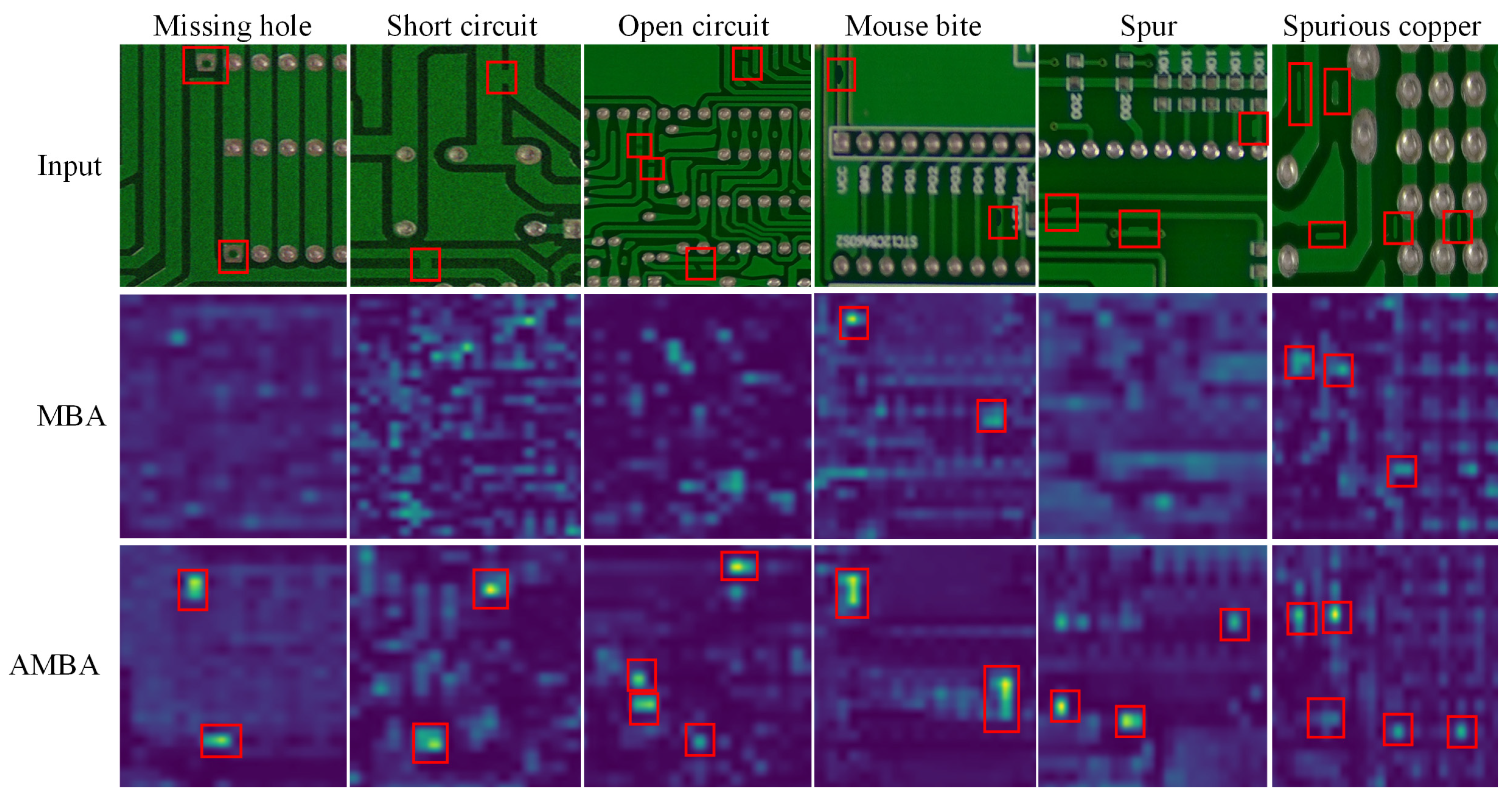
Meanwhile, we visualize and compare the feature maps output by the last layer of AMBA and MBA with average fixed weights. As can be seen from Figure 11, MBA with an average weighting method does not detect any defects, whether missing hole and spur of point defects or open circuit and short circuit of linear defects, and there are missing detection problems for spurious copper. Conversely, AMBA achieved detection of all defects, especially for open circuit with a complex background; the detection effect is excellent, which further verifies the superiority of using adaptive weighting.
Figure 11.
Comparison of MBA and AMBA defect detail feature maps.
4.3.2. Efficient Atrous Spatial Pyramid Pooling (EASPP)
To validate that EASPP can effectively solve the problem of feature information loss caused by SPPF, we conduct comparative visualizations of output features from structurally identical networks containing either EASPP or SPPF modules, as shown in Figure 12. It can be seen that after SPPF pooling, various types of defect information have different degrees of loss, resulting in missed detection, while the defect feature information extracted by EASPP is more abundant and accurate. This result further indicates that dilated convolution solves the problem of information loss in SPPF modules.
Figure 12.
Comparison of SPPF, SAPF, and EASPP feature maps.
Furthermore, to verify the effectiveness of replacing ECA with AMBA on the basis of ASPF, we compare the two modules only containing ASPF and EASPP; the results are shown in Figure 12. ASPF has the problem that defects cannot be differentiated from background noise in short circuit and has missing detection problems for spur. In contrast, the EASPP module can completely detect all defects, which not only effectively solves the problem of information loss, but also focuses attention on defect information, which better separates defect feature information from the background and improves the accuracy of model detection.
4.3.3. Bidirectional Feature Pyramid Network (BiFPN)
To demonstrate the effectiveness and generalization of the improved method, we designed comparative experiments for different types of defects. Considering that PAN and BiFPN are added in the process of feature fusion, we have listed the visualization results of each defect in the last layer output, as shown in Figure 13.
Figure 13.
Comparison of PAN and BiFPN defect detail feature maps.
It can be seen that there is information attenuation when the original PAN transmits the defect information to the detection head, and the complete defect information cannot be transmitted to the detection head part; in particular, the feature loss problem of tiny defects (mouse bite, spur, and open circuit) is particularly serious. The BiFPN used in this paper is basically consistent with real defects in transmitting defect feature information, and shows excellent detection results in all defect types. These results empirically confirm BiFPN advantages in preserving critical defect signatures.
The above experiments show that AMBA, EASPP, and BiFPN have significantly improved the detection accuracy of PCB defect detection, which can further optimize the performance of the YOLOv10 module, thus greatly improving the accuracy of PCB defect detection.
5. Conclusions
In this article, a novel YOLO-AEB network based on improved YOLOv10 for PCB defect detection was proposed for addressing the persistent challenge of detecting tiny defects in PCBs with complex background patterns. Firstly, the AMBA employs multidimensional feature importance weighting to suppress non-critical regions while adaptively amplifying defect signatures through dynamic channel-width-context dimension recalibration. Secondly, EASPP is designed to counteract multi-scale feature degradation inherent in conventional max pooling operations by integrating hybrid dilated convolutions with AMBA-driven attention prioritization. Finally, the BiFPN enhances shallow feature propagation through topologically optimized pathways and learnable weight allocation, thereby addressing the progressive information loss observed in traditional PAN implementations. The experimental results show that the improved method proposed in this paper is at the leading level in detection accuracy, which fully reflects the superiority and feasibility of the method.
Although the improved network model in this paper performs well in PCB defect detection accuracy, it has not yet achieved a significant improvement in detection speed. Therefore, in future research, we will further improve the detection accuracy of tiny defects and explore how to optimize the network to consider faster detection speed.
Author Contributions
Resources, Funding acquisition, Methodology, and Writing: C.D.; Methodology, Software, Validation, and Writing: Y.W., Z.W., and Y.Z.; Writing and Validation: X.S., W.Z., and S.W. All authors have read and agreed to the published version of the manuscript.
Funding
This work was supported in part by the National Natural Science Foundation of China under Grant 61865012, and by the Natural Science Foundation Jiangxi Province under Grant 20213AAG01012.
Data Availability Statement
The data used to support the findings of this study are available from the corresponding author upon request.
Conflicts of Interest
The authors declare no conflicts of interest.
References
- Zhou, W.; Li, C.; Ye, Z.; He, Q.; Ming, Z.; Chen, J.; Wan, F.; Xiao, Z. An Efficient Tiny Defect Detection Method for PCB With Improved YOLO Through a Compression Training Strategy. IEEE Trans. Instrum. Meas. 2024, 73, 1–14. [Google Scholar] [CrossRef]
- Ibrahim, Z.; Al-Attas, S.A.R.; Aspar, Z.; Mokji, M.M. Performance evaluation of wavelet-based PCB defect detection and localization algorithm. In Proceedings of the 2002 IEEE International Conference on Industrial Technology, 2002, IEEE ICIT, Bankok, Thailand, 11–14 December 2002; Volume 1, pp. 226–231. [Google Scholar]
- Tsai, D.-M.; Huang, C.-K. Defect Detection in Electronic Surfaces Using Template-Based Fourier Image Reconstruction. IEEE Trans. Compon. Packag. Manuf. Technol. 2019, 9, 163–172. [Google Scholar] [CrossRef]
- Wang, Y.; Sun, Y.; Zhang, W. Automatic Inspection of Small Component on Loaded PCB Based on Mean-Shift and Support Vector Machine. In Proceedings of the 2009 Fifth International Conference on Natural Computation, Tianjian, China, 14–16 August 2009; pp. 195–198. [Google Scholar] [CrossRef]
- Huang, Z.; Xiao, H.; Zhang, R.; Wang, H.; Zhang, C.; Shi, X. Multi-Scale Feature Pair Based R-CNN Method for Defect Detection. In Proceedings of the 2019 International Conference on Internet of Things (iThings) and IEEE Green Computing and Communications (GreenCom) and IEEE Cyber, Physical and Social Computing (CPSCom) and IEEE Smart Data (SmartData), Atlanta, GA, USA, 14–17 July 2019; pp. 46–51. [Google Scholar] [CrossRef]
- Liu, Y. An Improved Faster R-CNN for Object Detection. In Proceedings of the 2018 11th International Symposium on Computational Intelligence and Design (ISCID), Hangzhou, China, 8–9 December 2018; pp. 119–123. [Google Scholar] [CrossRef]
- Yin, S.; Li, H.; Teng, L.; Laghari, A.A.; Almadhor, A.; Gregus, M.; Sampedro, G.A. Brain CT image classification based on mask RCNN and attention mechanism. Sci. Rep. 2024, 14, 29300. [Google Scholar] [CrossRef]
- Ma, W.; Wang, X.; Yu, J. A Lightweight Feature Fusion Single Shot Multibox Detector for Garbage Detection. IEEE Access 2020, 8, 188577–188586. [Google Scholar] [CrossRef]
- Hussain, M. YOLO-v1 to YOLO-v8, the Rise of YOLO and Its Complementary Nature toward Digital Manufacturing and Industrial Defect Detection. Machines 2023, 11, 677. [Google Scholar] [CrossRef]
- Fan, F.; Wang, B.; Zhu, G.; Wu, J. Efficient Faster R-CNN: Used in PCB Solder Joint Defects and Components Detection. In Proceedings of the 2021 IEEE 4th International Conference on Computer and Communication Engineering Technology (CCET), Beijing, China, 13–15 August 2021; pp. 1–5. [Google Scholar] [CrossRef]
- Lian, J.; Wang, L.; Liu, T.; Ding, X.; Yu, Z. Automatic visual inspection for printed circuit board via novel Mask R-CNN in smart city applications. Sustain. Energy Technol. Assess 2021, 44, 101032. [Google Scholar] [CrossRef]
- Chaudhari, A.; Upganlawar, V.; Barve, T.; Vaidya, R.; Shelke, D. Analysis of YOLO V3 for Multiple Defects Detection in PCB. In Proceedings of the 2024 Parul International Conference on Engineering and Technology (PICET), Vadodara, India, 3–4 May 2024; pp. 1–6. [Google Scholar] [CrossRef]
- Ye, M.; Wang, H.; Xiao, H. Light-YOLOv5: A Lightweight Algorithm for Improved YOLOv5 in PCB Defect Detection. In Proceedings of the 2023 IEEE 2nd International Conference on Electrical Engineering, Big Data and Algorithms (EEBDA), Changchun, China, 24–26 February 2023; pp. 523–528. [Google Scholar] [CrossRef]
- Wang, Q.; Wu, B.; Zhu, P.; Li, P.; Zuo, W.; Hu, Q. ECA-Net: Efficient Channel Attention for Deep Convolutional Neural Networks. In Proceedings of the 2020 IEEE/CVF Conference on Computer Vision and Pattern Recognition (CVPR), Seattle, WA, USA, 13–19 June 2020; pp. 11531–11539. [Google Scholar] [CrossRef]
- Wang, X.; Zhang, X.; Zhou, N. Improved YOLOv5 with BiFPN on PCB Defect Detection. In Proceedings of the 2021 2nd International Conference on Artificial Intelligence and Computer Engineering (ICAICE), Hangzhou, China, 5–7 November 2021; pp. 196–199. [Google Scholar] [CrossRef]
- Yang, B.; Qu, Z. A PCB Defect Detection Algorithm Based on Improved Yolov7-tiny. In Proceedings of the 2023 IEEE 5th International Conference on Civil Aviation Safety and Information Technology (ICCASIT), Dali, China, 11–13 October 2023. [Google Scholar]
- Liu, Y.; Gao, C.; Song, B.; Liang, S. A Surface Defect Detection Algorithm for PCB Based on MobileViT-YOLO. In Proceedings of the 2023 China Automation Congress (CAC), Chongqing, China, 17–19 November 2023; pp. 6318–6323. [Google Scholar] [CrossRef]
- Hua, L. Motor PCB Defect Detection Algorithm Based on Improved YOLOv7-tiny. In Proceedings of the 2024 6th International Conference on Electronic Engineering and Informatics (EEI), Chongqing, China, 28–30 June 2024; pp. 272–275. [Google Scholar] [CrossRef]
- Lan, H.; Zhu, H.; Luo, R.; Ren, Q.; Chen, C. PCB Defect Detection Algorithm of Improved YOLOv8. In Proceedings of the 2023 8th International Conference on Image, Vision and Computing (ICIVC), Dalian, China, 27–29 July 2023. [Google Scholar]
- Hu, Y.; Wang, S.; Hong, Y.; Li, R. A YOLOv8s Model Integrating GELAN Module and HAT Attention for PCB Defect Detection. In Proceedings of the 2024 5th International Conference on Electronic Communication and Artificial Intelligence (ICECAI), Shenzhen, China, 31 May–2 June 2024; pp. 297–300. [Google Scholar] [CrossRef]
- Selvam, P.; Rajasekar, R.; Gunasundari, C.; Janu Priya, S.; Murugappan, M.; Chowdhury, M.E.H. YOLO-DefXpert: An Advanced Defect Detection on PCB Surfaces Using Improved YOLOv11 Algorithm. IEEE Access 2025, 13, 143085–143101. [Google Scholar] [CrossRef]
- Yin, X.; Zhao, Z.; Weng, L. MAS-YOLO: A Lightweight Detection Algorithm for PCB Defect Detection Based on Improved YOLOv12. Appl. Sci. 2025, 15, 6238. [Google Scholar] [CrossRef]
- Wu, H.; Lin, Y. A High-Performance and Enhanced Generalization Small Target Defect Detection Method for PCB Boards Based on YOLO-EMAC. IEEE Trans. Instrum. Meas. 2025, 74, 5042513. [Google Scholar] [CrossRef]
- Wang, A.; Chen, H.; Liu, L.; Chen, K.; Lin, Z.; Han, J.; Ding, G. YOLOv10: Real-Time End-to-End Object Detection. arXiv 2024, arXiv:2405.14458. [Google Scholar]
- Lu, G.; Zhang, W.; Wang, Z. Optimizing Depthwise Separable Convolution Operations on GPUs. IEEE Trans. Parallel Distrib. Syst. 2022, 33, 70–87. [Google Scholar] [CrossRef]
- Xiong, D.; Wen, Z.; Zhang, C.; Ren, D.; Li, W. BMNet: Enhancing Deepfake Detection Through BiLSTM and Multi-Head Self-Attention Mechanism. IEEE Access 2025, 13, 21547–21556. [Google Scholar] [CrossRef]
- Rezatofighi, H.; Zhu, T.; Kaskman, R.; Motlagh, F.T.; Shi, J.Q.; Milan, A.; Cremers, D.; Leal-Taixe, L.; Reid, I. Learn to Predict Sets Using Feed-Forward Neural Networks. IEEE Trans. Pattern Anal. Mach. Intell. 2022, 44, 9011–9025. [Google Scholar] [CrossRef] [PubMed]
- Lee, H.; Lee, J.-S.; Choi, H.-C. Parallelization of Non-Maximum Suppression. IEEE Access 2021, 9, 166579–166587. [Google Scholar] [CrossRef]
- Mao, M.; Lee, A.; Hong, M. Efficient Fabric Classification and Object Detection Using YOLOv10. Electronics 2024, 13, 3840. [Google Scholar] [CrossRef]
- Hu, H.; Tong, J.; Wang, H.; Lu, X. EAD-YOLOv10: Lightweight Steel Surface Defect Detection Algorithm Research Based on YOLOv10 Improvement. IEEE Access 2025, 13, 55382–55397. [Google Scholar] [CrossRef]
- Mayya, A.M.; Alkayem, N.F. Enhance the Concrete Crack Classification Based on a Novel Multi-Stage YOLOV10-ViT Framework. Sensors 2024, 24, 8095. [Google Scholar] [CrossRef]
- Mei, J.; Zhu, W. BGF-YOLOv10: Small Object Detection Algorithm from Unmanned Aerial Vehicle Perspective Based on Improved YOLOv10. Sensors 2024, 24, 6911. [Google Scholar] [CrossRef]
- Liao, L.; Song, C.; Wu, S.; Fu, J. A Novel YOLOv10-Based Algorithm for Accurate Steel Surface Defect Detection. Sensors 2025, 25, 769. [Google Scholar] [CrossRef]
- Niu, Z.; Zhong, G.; Yu, H. A review on the attention mechanism of deep learning. Neurocomputing 2021, 452, 48–62. [Google Scholar] [CrossRef]
- Qin, C.; Zhou, Z. YOLO-FGD: A fast lightweight PCB defect method based on FasterNet and the Gather-and-Distribute mechanism. J. Real-Time Image Proc. 2024, 21, 122. [Google Scholar] [CrossRef]
- Yuan, M.; Zhou, Y.; Ren, X.; Zhi, H.; Zhang, J.; Chen, H. YOLO-HMC: An Improved Method for PCB Surface Defect Detection. IEEE Trans. Instrum. Meas. 2024, 73, 2001611. [Google Scholar] [CrossRef]
- Huang, W.; Wen, J.; Gan, W.; Hu, L.; Luo, B. Neighborhood Correlation Enhancement Network for PCB Defect Classification. IEEE Trans. Instrum. Meas. 2023, 72, 2506111. [Google Scholar] [CrossRef]
- Yue, Z.; Li, X.; Zhou, H.; Wang, G.; Wang, W. Real-time recognition method for PCB chip targets based on YOLO-GSG. J. Real-Time Image Proc. 2025, 22, 44. [Google Scholar] [CrossRef]
- Bai, L.; Xu, W.H. Improved printed circuit board defect detection scheme. Sci. Rep. 2025, 15, 2389. [Google Scholar] [CrossRef]
- Li, G.; Zhao, S.; Zhou, M.; Li, M.; Shao, R.; Zhang, Z.; Han, D. YOLO-RFF: An Industrial Defect Detection Method Based on Expanded Field of Feeling and Feature Fusion. Electronics 2022, 11, 4211. [Google Scholar] [CrossRef]
- Cui, H.; Wei, Z. Multi-Scale Receptive Field Detection Network. IEEE Access 2019, 7, 138825–138832. [Google Scholar] [CrossRef]
- Hu, J.-F.; Sun, J.; Lin, Z.; Lai, J.-H.; Zeng, W.; Zheng, W.-S. APANet: Auto-Path Aggregation for Future Instance Segmentation Prediction. IEEE Trans. Pattern Anal. Mach. Intell. 2022, 44, 3386–3403. [Google Scholar] [CrossRef] [PubMed]
- Zhao, B.; Guo, A.; Ma, R.; Zhang, Y.; Gong, J. YOLOv8s-CFB: A lightweight method for real-time detection of apple fruits in complex environments. J. Real-Time Image Proc. 2024, 21, 164. [Google Scholar] [CrossRef]
- Christlein, V.; Spranger, L.; Seuret, M.; Nicolaou, A.; Král, P.; Maier, A. Deep Generalized Max Pooling. In Proceedings of the 2019 International Conference on Document Analysis and Recognition (ICDAR), Sydney, NSW, Australia, 20–25 September 2019; pp. 1090–1096. [Google Scholar] [CrossRef]
- He, K.; Zhang, X.; Ren, S.; Sun, J. Spatial Pyramid Pooling in Deep Convolutional Networks for Visual Recognition. IEEE Trans. Pattern Anal. Mach. Intell. 2015, 37, 1904–1916. [Google Scholar] [CrossRef] [PubMed]
- Huang, W.; Wei, P.; Zhang, M.; Liu, H. HRIPCB: A challenging dataset for PCB defects detection and classification. J. Eng. 2020, 2020, 303–309. [Google Scholar] [CrossRef]
Disclaimer/Publisher’s Note: The statements, opinions and data contained in all publications are solely those of the individual author(s) and contributor(s) and not of MDPI and/or the editor(s). MDPI and/or the editor(s) disclaim responsibility for any injury to people or property resulting from any ideas, methods, instructions or products referred to in the content. |
© 2025 by the authors. Licensee MDPI, Basel, Switzerland. This article is an open access article distributed under the terms and conditions of the Creative Commons Attribution (CC BY) license (https://creativecommons.org/licenses/by/4.0/).