Abstract
Flexible and high-sensitive capacitive sensors are demanded to detect pressure distribution and/or tactile information on a curved surface, hence, wide varieties of polymer-based flexible MEMS sensors have been developed. High-sensitivity may be achieved by increasing the capacitance of the sensor using solid dielectric material while it deteriorates the flexibility. Using air as the dielectric, to maintain the flexibility, sacrifices the sensor sensitivity. In this paper, we demonstrate flexible and highly sensitive capacitive sensor arrays that encapsulate highly dielectric liquids as the dielectric. Deionized water and glycerin, which have relative dielectric constants of approximately 80 and 47, respectively, could increase the capacitance of the sensor when used as the dielectric while maintaining flexibility of the sensor with electrodes patterned on flexible polymer substrates. A reservoir of liquids between the electrodes was designed to have a leak path, which allows the sensor to deform despite of the incompressibility of the encapsulated liquids. The proposed sensor was microfabricated and demonstrated successfully to have a five times greater sensitivity than sensors that use air as the dielectric.
1. Introduction
Recently applications of high sensitive pressure sensors include tactile sensation for humanoid robots and medical instruments, which can achieve seamless and, more importantly, safe physical interaction with environment; including human contact [1,2,3,4,5,6]. Many sensing principles have been proposed to detect pressure distribution applied on contact surfaces. Conductive polymer, containing conductive particles, was used for the pressure sensors which recognized pressure by detecting variation of the resistance [7,8]. Vision-based sensors monitor deformation of the object and deduce the pressure distribution applied [9,10]. An attempt was made to enhance the piezoresistive sensor sensitivity by placing a polymer thin film mimicking the epidermal ridge structures on a finger skin [11]. Capacitive sensors are among one of the frequently used pressure sensors since they have simple structures composed of electrodes and a dielectric and good compatibility with MEMS fabrication technologies. Making an array of small sensors can be easily achieved with MEMS techniques [4,5,6,12,13,14,15,16,17,6,12], which enable tactile sensing with a fine spatial resolution. These capacitive sensors require not only high sensitivity but also flexibility to detect the pressure applied to curved surfaces while conforming to the surfaces. Although wide varieties of silicon-based MEMS capacitive sensors have been developed [17,18,19,20,21,22], brittleness of silicon makes the sensors difficult to conform to a curved surface. Hence, polymer-based flexible sensors have been proposed and demonstrated [3,4,5,6,15,16,23,24,25,26,27,6,15,16,23].
Since air has a relatively low dielectric constant, dielectric material is sandwiched by the electrodes to enhance the sensitivity of capacitive sensors, amongst which solid material was used [3,18,28,29,30]. However, the solid dielectric impairs the sensors flexibility and often resulted in electrification. Recently, MEMS devices encapsulating liquid inside have been developed, which exploits unique characteristics of liquids that are deformable and can form spherical shape due to the surface tension [31,32,33,34,35]. Liquid encapsulation processes have also been developed, including deposition of parylene directly onto nonvolatile liquid [31], bonding-in-liquid technique (BiLT) [33,34,35], and sealing with gold wire [36].
In this paper, we propose a polymer-based capacitive sensor that uses deionized (DI) water and glycerin as the dielectric as depicted in Figure 1. The capacitance of the electrodes increases when pressure is applied to the device. DI water is liquid and has a high relative dielectric constant of approximately 80.4, i.e., the proposed sensor has a high sensitivity that can be defined as the ratio of the variation in the capacitance to the applied pressure while maintaining its flexibility [37]. Glycerin also has a high relative dielectric as 47 and is a non-volatile liquid, which contributes to the long-term stability of the device. We used PDMS (polydimethyl siloxane) as a structural material of the device. Since the adhesion of metal electrodes and wirings to a PDMS layer is poor, we used a polyimide film as an intermediate layer. We designed an escape reservoir that allows incompressible liquid, such as DI water and glycerin, to move from the cavity between the electrodes when pressure is applied to the sensor and, in turn, allows the flexible sensors to deform to vary the capacitance. We microfabricated the proposed sensor and experimentally demonstrated the high sensitivity as well as flexibility.
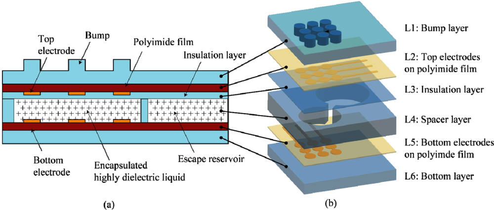
Figure 1.
(a)A schematic cross-sectional image of the proposed sensor.(b) An exploded drawing of the sensor elements.
2. Design
The device consists of six layers as shown in Figure 1. A bump layer (L1) is made of PDMS and has bumps 300 µm in height and 1 mm in diameter to enhance a spatial resolution of the sensor. The spatial resolution of 1 mm is comparable to the resolution of human tactile sensation. Top and bottom electrodes layers (L2 and L5) contain copper electrodes 18 µm in thickness deposited on polyimide films. 3 by 3 pairs of circular electrodes 1 mm diameter with a gap of 500 µm are designed to be aligned with the bumps of L1. The large gap leads to low capacitance and thus, low sensitivity of the device whereas the small gap leads to high likelihood of chamber collapse given the flexible polymer structures, which may limit the detectable pressure range. Since the 9 electrodes on L2 and L5 are not mechanically isolated, the resolution to discriminate the arbitrary shapes is determined by the bump geometry. The width of metal wiring is designed to be 200 µm. Since adhesion between copper and PDMS is poor, in particularly, with a presence of deformation as we discuss in the following Section 3.1, a photosensitive polyimide 25 µm in thickness is used as an intermediate layer to enhance the adhesion without losing the flexibility. An insulation layer (L3), which is 15 µm in thickness and is also made of PDMS, is formed to assure the electrical isolation between the electrodes when large load is applied to the sensor and the L3 and L5 is brought into contact. The spacer layer (L4) determines the gap between the electrodes as well as volume of the liquid to be encapsulated. The spacer layer contains a cylindrical chamber located between the electrodes and an escape reservoir for the liquid as shown in Figure 1(b). The escape reservoir and the chamber between the electrodes are filled with liquid. When loads are applied to the sensor parts and the chamber deforms, the liquid in the chamber flows into the escape reservoir. The escape reservoir is designed to have a cross-sectional area of 113 mm2, which is 64 times larger than the cross-sectional area of the bumps 1.77 mm2. Due to the large discrepancy in the cross-sectional areas, the membrane of the escape reservoir deforms to compensate the change in the reservoir volume while generating negligible resistive force. Without the reservoir, given the incompressible nature of the liquid (DI water and glycerin were used in this work), deformation of the chamber is suppressed, which would deteriorate the sensor sensitivity. When the load is released, the resistive force pushes back the liquid to the original location.
In order to validate the operation of the proposed sensor, the deformation of the bump layer was simulated with a commercial FEM solver (ANSYS ED 9.0). The element type was defined as a large-deformable material and the analysis was conducted using a liner elastic deformation mode. The model membrane was constructed with the ANSYS design modeler and the material properties used in the simulation were 3.5 MPa for the Young’s modulus and 0.499 for Poisson’s ratio [38]. The boundary condition for circular side of the model was fixed in all directions. Pressure was applied onto the bump mounted on the center electrode. When pressure of 200 kPa is applied onto a bump as shown in Figure 2(a), the liquid is pushed into the escape reservoir, which in turn, deforms the upper layer with half elliptical shape as shown in Figure 2 (b). When 200 kPa is applied onto the bump, the transferred fluid volume is calculated to be 7.71 × 10⁻⁶ mm3. This corresponds to the displacement of the upper layer of the escape reservoir of 102 µm. The resistive pressure is calculated to be 70 Pa, only 0.035% of the applied pressure and considered to be negligible.
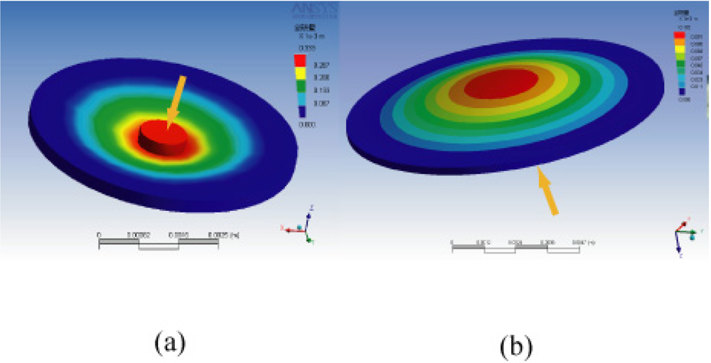
Figure 2.
Three dimensional FEM model to validate the deformation of (a) the bump layer and (b) the layers above the escape reservoir.
3. Experimental Section
3.1. Fabrication
The proposed flexible capacitive sensor is mostly composed of PDMS, while electrodes are patterned on the bump and bottom layers. When copper was vapor deposited directly on PDMS, crack and unevenness in the deposited layer were observed due to the heat involved with the deposition process. We used a photosensitive polyimide film 25 µm in thickness with a 18-µm-thick copper layer (MC18-25-00FRM, Nippon Steel Chemical Co., Ltd.) to pattern the electrodes without losing flexibility of the sensor. The photosensitive polyimide is a negative type photosensitive resin and hardens when a UV light of 200 nm~400 nm in wavelength is irradiated. It maintains its flexibility after a curing process. The width of copper wiring was designed to be 200 µm. Adhesion between the copper and polyimide layers was strong enough to allow them to deform without any fractures.
Six layers were fabricated individually and then, bonded together. This procedure is effective in microfabricating three-dimensional structures [39,40]. The electrodes and wirings were fabricated and patterned on a polyimide film via photolithography processes. For both upper and lower electrode layers, a positive photoresist (AZ7320, Microchem Corp.) was spin-coated on the copper layer after making the surface hydrophobic with hexamethyldisilazane (OAP, Tokyo Ohka Kogyo Co., Ltd.). The photoresist was developed in a developing solution (AZ400K, Microchem Corp.) after exposure. Copper layer was etched by ferric chloride (FeCl3) (H-1000A, Sunhayato Co., Ltd.). To form the spacer and bump layers, photolithographically patterned negative photoresist (SU-8 2075, Microchem Corp.) was used as the mold. The height of the bump and the spacer were designed to be 300 µm and 500 µm, respectively. The viscosity of the SU-8 2000 series is so high that their maximum adjustable thickness is less than 300 µm. Therefore, to make the sufficiently high SU-8 mold of the spacer layer, we iterated spin-coating and curing processes. PDMS prepolymer (Sylgard 184, Dow Corning) was mixed with the curing agent with a ratio of 10 to 1 and was spin-coated on the substrate to have thickness of 300 µm for the bump layer and 500 µm for the spacer layer, respectively. The PDMS was cured on a hotplate at 100 °C for 24 h. After the cure, they were peeled off and unnecessary parts were cut off. The fabricated spacer layer and bump layer are shown in Figure 3(a,b). The insulation layer 15 µm in thickness made of PDMS was directly spin-coated on the upper electrode. To form the bottom layer, PDMS was spin-coated on a glass substrate with fluorocarbon polymer, which attenuated adhesion of the PDMS to the substrate and facilitated the peeling-off process. Amorphous fluorocarbon CYTOP type B (Asahi Glass Co. Ltd.) and then, CYTOP type A were spin-coated and cured sequentially on a glass substrate. CYTOP type B was used to enhance adhesion between CYTOP type A and the glass substrate. The thickness of the membrane was measured with a laser microscope (VK-9700, KEYENCE Co. Ltd.).
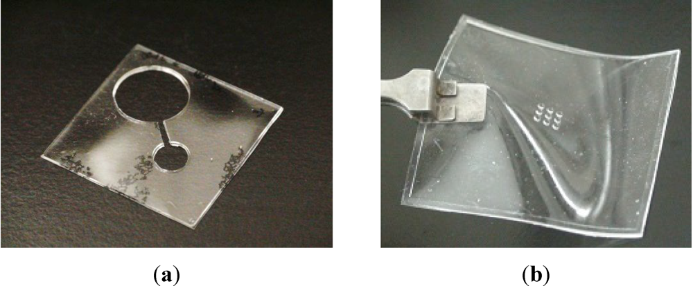
Figure 3.
Photos of (a) the spacer layer (L4) and (b) the bump layer (L1).
The fabricated six layers were bonded together as shown in Figure 4. PDMS layers were bonded to polyimide films after oxygen plasma treatment by a plasma etcher (SEDE-P, Meiwafosis Co., Ltd.) as shown in Figure 4(a,b). In order to encapsulate liquid without interfusion of air bubbles, the upper electrode layer and the spacer layer was bonded using BiLT (bonding in liquid technique) [31,32], as shown in Figure 4(c). UV curable resin (3164 ThreeBond UV-curable resin, Threebond corp.) was used as glue. First, a UV-curable resin was spin-coated on a glass substrate. It was transferred to the bonding surface of the spacer layer by stamping the spacer layer on the resin. The electrode layers and the spacer layer were bonded in liquid while UV light was exposed. Since the bonding was conducted in liquid, no interfusion of air bubbles and deformation of the flexible substrates caused by their own weights were observed. The encapsulation process was conducted at room temperature and under atmospheric pressure.
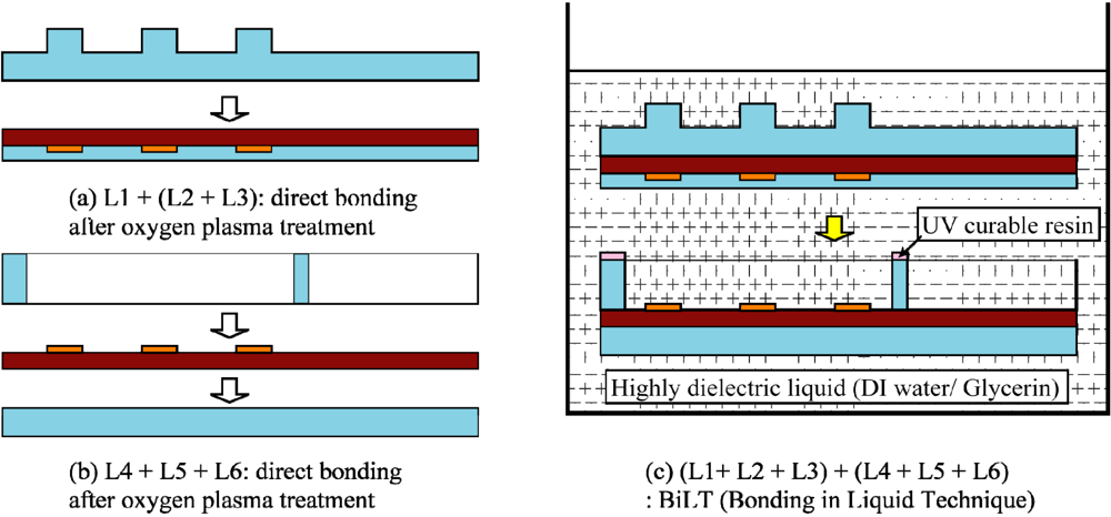
Figure 4.
Assembling process of the proposed sensor. (a,b) bonding of PDMS layers to the polyimide films and (c) bonding of all layers while encapsulating highly dielectric liquid by using BiLT.
3.2. Experimental Results
The fabricated device is shown in Figure 5(a). The sensor containing liquids inside was flexible and could afford a large deformation without fractures as shown in Figure 5(b). The completed capacitive tactile sensor was tested using an experimental set up as shown in Figure 6. A commercially available digital-to-capacitance converter (AD7746, Analog Devices Ltd.) with a resolution of 4 aF was used to measure the capacitance. A sharp tip (tip diameter of 100 µm) was attached to a z-axis stage controller (PAT-001, Shigma Kohki Co., Ltd.) with a resolution of 2 µm. It pressed down the sensor while the displacement of the tip and the applied pressure was recorded by a digital force gauge (ZP-50N, Imada Corp.) with a resolution of 10 mN. All the instruments were arranged on an anti-static electricity mat to reduce noise.
Displacement of the tip as a function of the applied pressure when DI water was and was not encapsulated into the sensor is shown in Figure 7 along with the simulated results. The experimental results showed good agreement with the simulation as shown in Figure 7, which verified that the device was successfully manufactured as designed. Discrepancy between the experiments and simulation is considered to originate from non-linear characteristics of polymer material. Due to the incompressible nature of DI water, the displacement when the device contained DI water was found to be less than when DI water was not encapsulated. However, the escape reservoir successfully suppressed the difference to less than 10%.
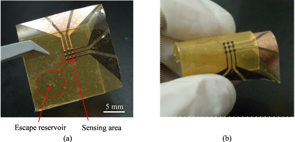
Figure 5.
(a)Fabricated sensor.(b) It did not fracture after it was bent.
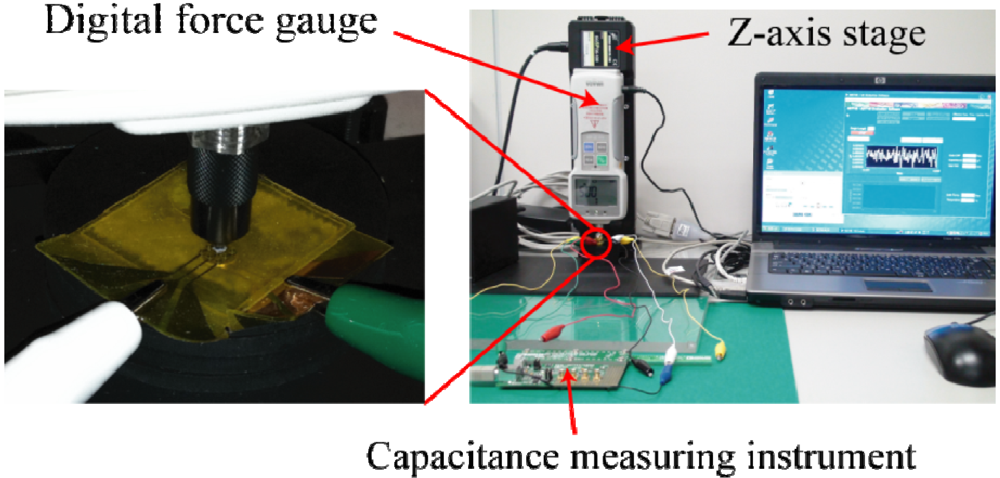
Figure 6.
Experimental setup.
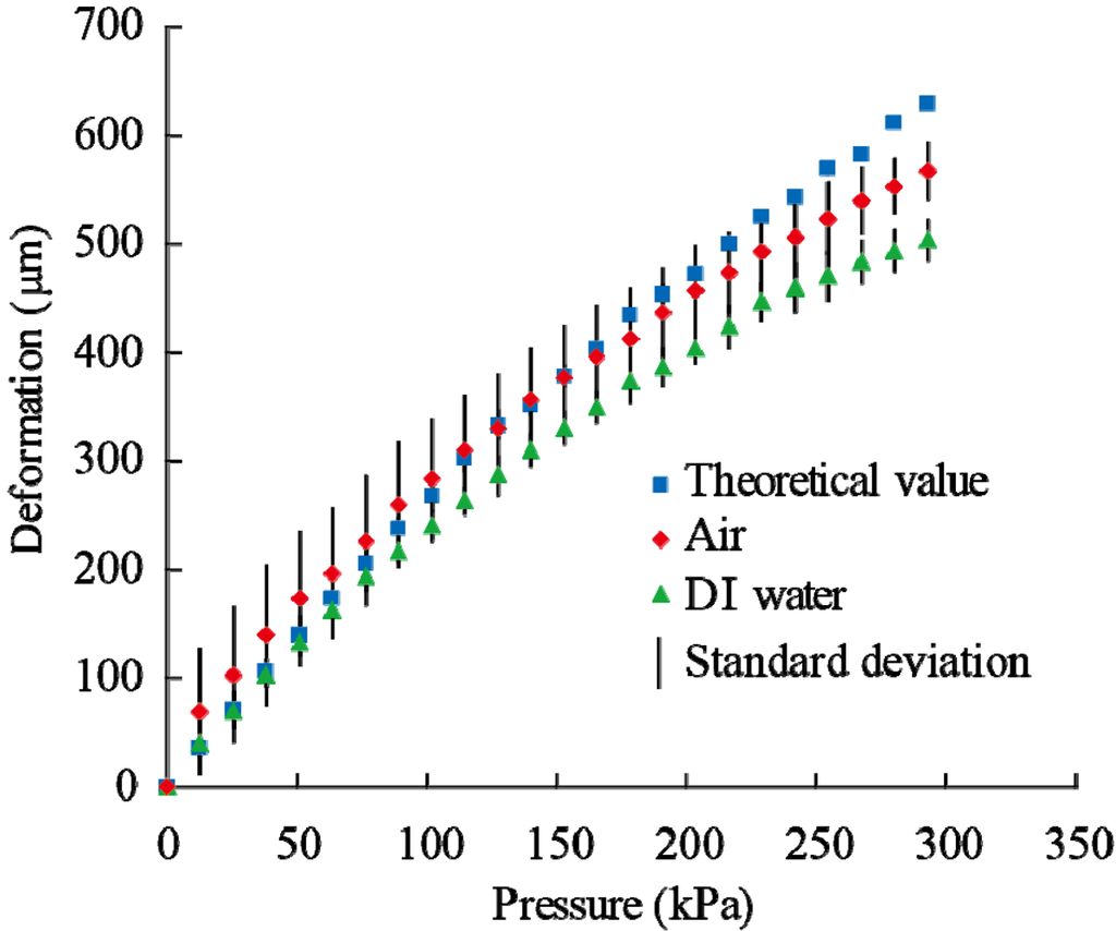
Figure 7.
Calculated and experimentally deduced deformation of the device with and without DI water as a function of the applied pressure. The error bars represent standard deviation of the results (N = 3).
The increase in the capacitance of the center cell #5 of the devices with air, DI water, and glycerin as the dielectric is shown in Figure 8 when the pressure upto 300 kPa with a step of 10 kPa was applied to the center bump. The experiments showed a liner response of the capacitance increase to the applied pressure when the pressure was below 100 kPa. The capacitance variation C−C0 [pF] of the device with DI water was approximately expressed as:
C−C0 =4.5 × 10⁻⁴σ
where σ [kPa] was the applied pressure. The capacitance increased not linearly but monotonously at the applied pressure greater than 100 kPa. The encapsulated liquids successfully augmented the increase. In particular, DI water could successfully augment the sensor sensitivity by a factor of 5. Augmentation did not reach the relative permittivity of the encapsulated liquid. This is considered to be due to not only the suppressed deformation by the incompressible liquid but also the parasitic capacitance. The device with DI water showed noisier signals than that with glycerin. Given that the volatility is one of the characteristic differences in the material property between DI water and glycerin, we consider that vaporization and permeation into porous PDMS of DI water was the major source of the errors. This also leads to decrease in DI water in the chamber and deterioration of the device performance. It was reported that parylene deposition successfully sealed the PDMS structures without loss of flexibility [41]. This treatment may help to enhance the device performance. These effects were difficult to be quantified and therefore, the sensor needs to be experimentally calibrated.
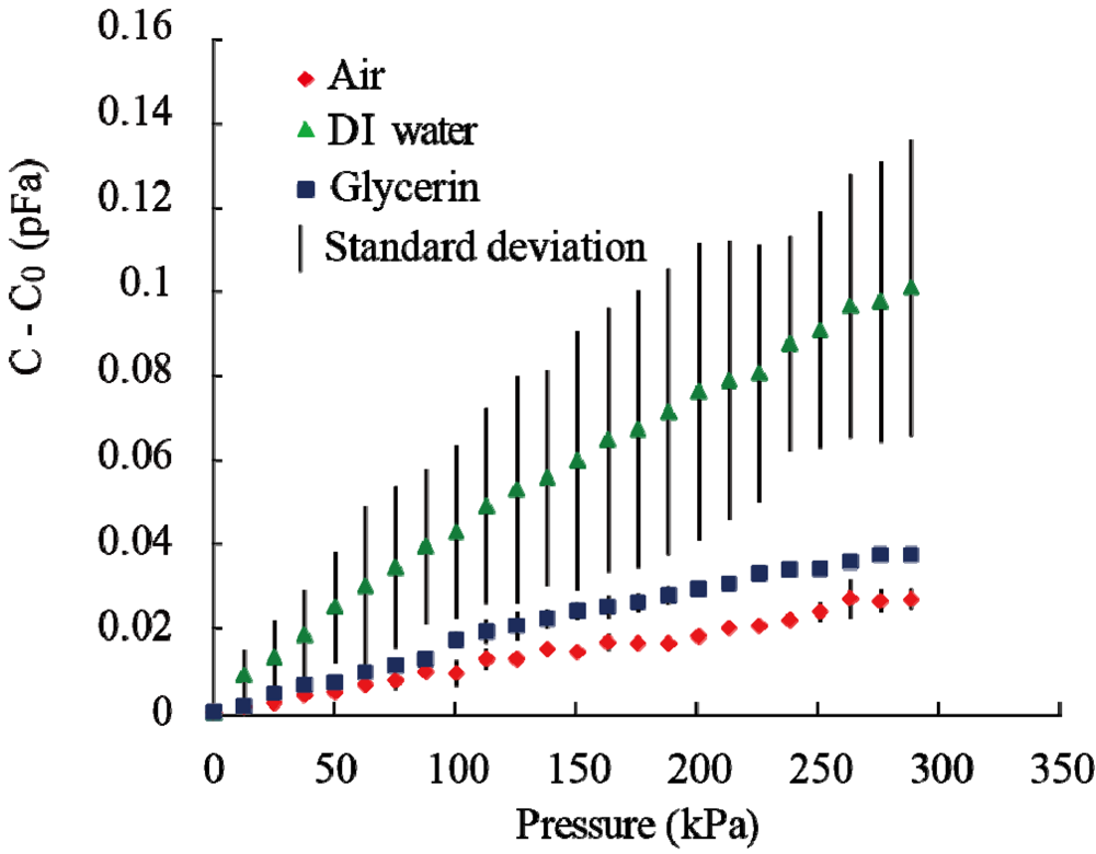
Figure 8.
Increase of the capacitance with respect to the applied pressure. The encapsulated liquid successfully enhanced the sensor sensitivity.
Next, we attempted to detect a distributed pressure using a 3 × 3 array of the sensors. Pressure was applied onto the device containing DI water by a sphere 5.5 mm in radius attached to a z-axis stage as shown in Figure 9(a,b). The center of the sphere was aligned to the center of the cell #5 as shown in Figure 9(c). In the experiment, first, the sphere was brought down until it reached the center cell. Then the stage was lowered by 200 µm. Figure 10 shows the capacitance variations of the 9 cells, where the gray scale corresponds to the normalized capacitance variation by that of cell #5. The measured capacitance change can be converted into the applied pressure using the results obtained by the prior experiment. The microfabricated capacitive sensor containing 9 cells successfully detected the load and distributed pressure with a spatial resolution of the cell size. Cells #6 and #8 showed slightly greater capacitance variation than cells #2 and #4, which were derived from non-symmetric geometry of the sensor due to the escape reservoir. Symmetric designs including the paths for the incompressible encapsulated liquid may be more preferable.
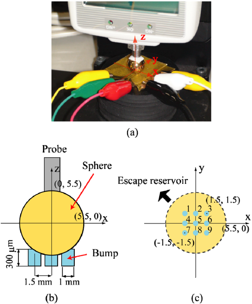
Figure 9.
(a) A sphere 5.5 mm in radius was pressed onto the sensor. Coordinate views from(b)side and(c) top.
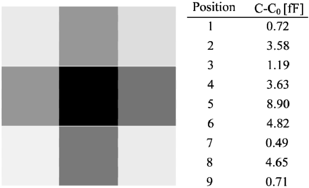
Figure 10.
Capacitance variation of the 9 cells when a distributed pressure was applied with a sphere 5.5 mm in radius.
4. Conclusions
We proposed and developed a capacitive sensor encapsulating highly dielectric liquid as the dielectric. The liquid enhances the sensitivity while maintaining flexibility of the sensor made of pliable polymer material. The escape reservoir was designed to allow the encapsulated liquid to escape from the sensing area, which enables the sensor to deform to the same extent as that achieved without liquid. We successfully fabricated the proposed sensor by exploiting soft lithography and the bonding-in-liquid technique. Experiments revealed that the sensor encapsulating DI water exhibited sensitivity five times greater than using air as the dielectric while maintaining the flexibility. Experimental calibration was necessary to deduce the relationship between the capacitance variation and the applied load since unknown parameters, including parasitic capacitance and permeation of the liquid into the porous PDMS, were difficult to be quantified. Three by three sensor cells successfully detected the distributed pressure.
Acknowledgments
This work was supported in part by Ministry of Education, Culture, Sports, Science and Technology (MEXT), Grant-in-Aid for Young Scientists (B) (21760202), in part by the Ministry of Internal Affairs and Communications (MIC), Strategic Information and Communications R&D Promotion Programnme (SCOPE) (092103005), and in part by Japan Science and Technology Agency (JST), PRESTO (Precursory Research for Embryonic Science and Technology), Information Environment and Humans.
References
- Eltaib, M.E.H.; Hewit, J.R. Tactile sensing technology for minimal access surgery—A review. Mechatronics 2003, 13, 1163–1177. [Google Scholar]
- Zhu, F.; Spronck, J.W. A capacitive tactile sensor for shear and normal force measurements. Sens. Actuat. A 1992, 31, 115–120. [Google Scholar]
- Hoshi, T.; Shinoda, H. Robot Skin based on Touch-Area-Sensitive Tactile Element. In Proceedings of the 2006 IEEE International Conference on Robotics and Automation, Orlando, FL, USA, 15–19 May 2006; pp. 3463–3468.
- Cheng, M.-Y.; Lin, C.-L.; Yang, Y.-J. Tactile and Shear Stress Sensing Array Using Capacitive Mechanisms with Floating Electrodes. In Proceedings of 2010 IEEE 23rd International Conference on Micro Electro Mechanical Systems (MEMS), Wanchai, Hong Kong, 24–28 January 2010; pp. 228–231.
- Lee, H.K.; Chung, J.; Chang, S.-I.; Yoon, E. Normal and shear force measurement using a flexible polymer tactile sensor with embedded multiple capacitors. J. Microelectromech. Syst. 2008, 17, 934–942. [Google Scholar] [CrossRef]
- Lee, H.K.; Chang, S.-I.; Yoon, E. A flexible polymer tactile sensor: Fabrication and modular expandability for large area deployment. J. Microelectromech. Syst. 2006, 15, 1681–1686. [Google Scholar] [CrossRef]
- Shimojo, M.; Namiki, A.; Ishikawa, M.; Makino, R.; Mabuchi, K. A tactile sensor sheet using pressure conductive rubber with electrical-wires stitched method. IEEE Sens. J. 2004, 4, 589–596. [Google Scholar]
- Castellanos-Ramos, J.; Navas-González, R.; Macicior, H.; Sikora, T.; Ochoteco, E.; Vidal-Verdú, F. Tactile sensors based on conductive polymers. Microsyst. Technol. 2010, 16, 765–776. [Google Scholar]
- Begej, S. Planar and finger-shaped optical tactile sensors for robotic applications. IEEE J. Robot. Autom. 1988, 4, 472–484. [Google Scholar]
- Watanabe, N.; Moriyama, N. Grip force control using vision-based tactile sensor for dexterous handling. Eur. Robot. Symp. 2008, 44, 113–122. [Google Scholar]
- Zhang, Y.; Miki, N. Sensitivity enhancement of a micro-scale biomimetic tactile sensor with epidermal ridges. J. Micromech. Microeng. 2010, 20. [Google Scholar] [CrossRef]
- Lee, M.H.; Nicholls, H.R. Review article tactile sensing for mechatronics—A state of the art survey. Mechatronics 1999, 9, 1–31. [Google Scholar]
- Dahiya, R.S.; Metta, G.; Valle, M.; Sandini, G. Tactile sensing—From humans to humanoids. Robotics 2010, 26, 1–20. [Google Scholar]
- De Souza, R.J.; Wise, K.D. A Very High Density Bulk Micromachined Capacitive Tactile Imager. In Proceedings of the International Conference on Solid State Sensors and Actuators (TRANSDUCERS ’97), Chicago, IL, USA, 16–19 June 1997; pp. 1473–1476.
- Peng, P.; Rajamani, R.; Erdman, A.G. Flexible tactile sensor for tissue elasticity measurements. J. Microelectromech. Syst. 2009, 18, 1226–1233. [Google Scholar]
- Kim, H.-K.; Lee, S.-G.; Han, J.-E.; Kim, T.-R.; Hwang, S.-U.; Ahn, S.D.; You, I.-K.; Cho, K.-I.; Song, T.-K.; Yun, K.-S. Transparent and Flexible Tactile Sensor for Multi Touch Screen Application with Force Sensing. In Proceedings of the International Actuators and Microsystems Conference on Solid-State Sensors, (TRANSDUCERS 2009), Denver, CO, USA, 21–25 June 2009; pp. 1146–1149.
- Ko, C.-T.; Wu, J.-P.; Wang, W.-C.; Huang, C.-H.; Tseng, S.-H.; Chen, Y.-L.; Lu, M.S.-C. A Highly Sensitive CMOS-MEMS Capacitive Tactile Sensor. In Proceedings of the 2006 IEEE 19th International Conference on Micro Electro Mechanical Systems (MEMS), Istanbul, Turkey, 22–26 January 2006; pp. 642–645.
- Wibbeler, J.; Pfeifer, G.; Hietschold, M. Parasitic charging of dielectric surfaces in capacitive microelectromechanical systems (MEMS). Sens. Actuat. A 1998, 71, 74–80. [Google Scholar]
- Fujimori, T.; Hanaoka, Y.; Fukuda, H. Above-IC Integration of Capacitive Pressure Sensor Fabricated with CMOS Interconnect Processes. In Proceedings of the 2007 IEEE 19th International Conference on Micro Electro Mechanical Systems (MEMS), Hyogo, Japan, 21-25 January 2007; pp. 43–46.
- Salo, T.; Kirstein, K.-U.; Sedivy, J.; Grunenfelder, J.; Vancura, T.;Zund, G; Baltes, H. Continuous blood pressure monitoring utilizing a CMOS tactile sensor. Eng. Med. Biol. Soc. 2004, 3, 23226–23229. [Google Scholar]
- Hezarjaribi, Y.; Hamidon, M.N.; Keshmiri, S.H.; Bahadorimehr, A.R. Capacitive Pressure Sensors based on MEMS, Operating in Harsh Environments. In Proceedings of the 2008 IEEE International Conference on Semiconductor Electronics, Johor Bahru, Malaysia, 25-27 November 2008; pp. 184–187.
- Wang, S.; Feng, Y. Micro Capacitive Vacuum Sensor Based on MEMS. In Proceedings of the 5th IEEE International Conference on Nano/Micro Engineered and Molecular Systems (NEMS), Xiamen, China, 20–23 January 2010; pp. 1160–1164.
- Cheng, M.-Y.; Tsao, C.-M.; Lai, Y.-T.; Yang, Y.-J. A Novel Highly-Twistable Tactile Sensing Array Using Extendable Spiral Electrodes. In Proceedings of the 2009 IEEE 21th International Conference on Micro Electro Mechanical Systems (MEMS), Sorrento, Italy, 25–29 January 2009; pp. 92–95.
- Noda, K.; Hoshino, K.; Matsumoto, K.; Shimoyama, I. A shear stress sensor for tactile sensing with the piezoresistive cantilever standing in elastic material. Sens. Actuat. A 2006, 127, 295–301. [Google Scholar]
- Shimojo, M.; Namiki, A.; Ishikawa, M.; Makino, R.; Mabuchi, K. A tactile sensor sheet using pressure conductive rubber with electrical-wires stitched method. IEEE Sens. J. 2004, 4, 589–596. [Google Scholar]
- Kerpa, O.; Weiss, K.; Worn, H. Development of a Flexible Tactile Sensor System for a Humanoid Robot. In Proceedings of the 2003 IEEE/RSJ International Conference on Intelligent Robots and Systems, Nice, France, 22–26 September 2003; pp. 1–6.
- Engel, J.; Chen, J.; Liu, C. Development of polyimide flexible tactile sensor skin. J. Micromech. Microeng. 2003, 13, 359–366. [Google Scholar]
- Huan, X.-D.; Huan, J.-Q.; Qin, M.; Huan, Q.-A. A Fully Integrated Capacitive Pressure Sensor with High Sensitivity. In Proceedings of the IEEE Sensors 2007 Conference, Atlanta, GA, USA, 28–31 October 2007; pp. 1052–1055.
- Shkel, Y.M.; Ferrier, N.J. Electrostriction enhancement of solid-state capacitance sensing. Mechatronics 2003, 8, 318–325. [Google Scholar]
- Thakur, O.P.; Singh, A.K. Modeling of Capacitive Sensor Filled with Elastic Dielectrics and Its Advantages. In Proceedings of the 3rd International Conference on Sensing Technology, Tainan, Taiwan, 30 November–3 December 2008; pp. 467–471.
- Khiem, N.B.; Matsumoto, K.; Shimoyama, I. Polymer thin film deposited on liquid for varifocal encapsulated liquid lenses. Appl. Phys. Lett. 2008, 93. [Google Scholar] [CrossRef]
- Kim, H.; Najafi, K. An Electrically-Driven, Large-Deflection, High-Force, Micro Piston Hydraulic Actuator Array for Large-Scale Microfluidic Systems. In Proceedings of the 2009 IEEE 21th International Conference on Micro Electro Mechanical Systems (MEMS), Sorrento, Italy, 25–29 January 2009; pp. 483–486.
- Arouette, X.; Matsumoto, Y.; Ninomiya, T.; Okayama, Y.; Miki, N. Dynamic characteristics of a hydraulic amplification mechanism for large displacement actuators systems. Sensors 2010, 10, 2946–2956. [Google Scholar]
- Ninomiya, T.; Okayama, Y.; Matsumoto, Y.; Arouette, X.; Osawa, K.; Miki, N. MEMS-based hydraulic displacement amplification mechanism with completely encapsulated liquid. Sens. Actuat. A 2011, 166, 277–282. [Google Scholar]
- Okayama, Y.; Nakahara, K.; Arouette, X.; Ninomiya, T.; Matsumoto, Y.; Orimo, Y.; Hotta, A.; Omiya, M.; Miki, N. Characterization of a bonding-in-liquid technique for liquid encapsulation into MEMS devices. J. Micromech. Microeng. 2010, 20. [Google Scholar] [CrossRef]
- Antelius, M.; Fischer, A.C.; Niklaus, F.; Stemme, G.; Roxhed, N. Hermetic Integration of Liquids in MEMS by Room Temperature, High-Speed Plugging of Liquid-Filled Cavities at Wafer Level. In Proceedings of the 2011 IEEE 24th International Conference on Micro Electro Mechanical Systems (MEMS), Cancun, Mexico, 23–27 January 2011; pp. 356–359.
- Hotta, Y.; Zhang, Y.; Miki, N. Flexible Distributed Capacitive Sensor with Encapsulated Ferroelectric Liquid. In Proceedings of the 2011 IEEE 24th International Conference on Micro Electro Mechanical Systems (MEMS), Cancun, Mexico, 23–27 January 2011; pp. 573–576.
- Fuard, D.; Tzvetkova-Chevolleau, T.; Decossas, S.; Tracqui, P.; Schiavone, P. Optimization of poly-di-methyl-siloxane (PDMS) substrates for studying cellular adhesion and motility. Microelectron. Eng. 2008, 85, 1289–1293. [Google Scholar]
- Miki, N.; Teo, C.J.; Ho, L.C.; Zhang, X. Enhancement of rotordynamic performance of high-speed micro-rotors for power MEMS applications by precision deep reactive ion etching. Sens. Actuat. A 2003, 104, 263–267. [Google Scholar]
- Miki, N. Wafer bonding techniques for MEMS. Sens. Lett. 2005, 3, 263–273. [Google Scholar]
- Sawano, S.; Naka, K.; Werber, A.; Zappe, H.; Konishi, S. Sealing Method of PDMS as Elastic Material for MEMS. In Proceedings of the 2008 IEEE 21st International Conference on Micro Electro Mechanical Systems (MEMS), Tucson, AZ, USA, 13–17 January 2008; pp. 419–422.
© 2012 by the authors; licensee MDPI, Basel, Switzerland. This article is an open-access article distributed under the terms and conditions of the Creative Commons Attribution license (http://creativecommons.org/licenses/by/3.0/).