Article

Enhanced UVC Responsivity of Heteroepitaxial α-Ga2O3 Photodetector with Ultra-Thin HfO2 Interlayer

by
SiSung Yoon
1,
SeungYoon Oh
1,
GyuHyung Lee
1,
YongKi Kim
2,
SunJae Kim
3,
Ji-Hyeon Park
3,
MyungHun Shin
2,
Dae-Woo Jeon
3 and
GeonWook Yoo
1,*
1
Department of Intelligent Semiconductor, Soongsil University, Seoul 06938, Republic of Korea
2
Department of Electronics and Information Engineering, Korea Aerospace University, Goyang 10540, Republic of Korea
3
Korea Institute of Ceramic Engineering & Technology, Jinju 52851, Republic of Korea
*
Author to whom correspondence should be addressed.
Micromachines 2025, 16(7), 836; https://doi.org/10.3390/mi16070836
Submission received: 10 June 2025 / Revised: 18 July 2025 / Accepted: 19 July 2025 / Published: 21 July 2025
(This article belongs to the Special Issue Photodetectors and Their Applications)

Abstract

In this study, the influence of HfO2 interlayer thickness on the performance of heteroepitaxial α-Ga2O3 layer-based metal–insulator–semiconductor–insulator–metal (MISIM) ultraviolet photodetectors is examined. A thin HfO2 interlayer enhances the interface quality and reduces the density of interface traps, thereby improving the performance of UVC photodetectors. The fabricated device with a 1 nm HfO2 interlayer exhibited a significantly reduced dark current and higher photocurrent than a conventional metal–semiconductor–metal (MSM). Specifically, the 1 nm HfO2 MISIM device demonstrated a photocurrent of 2.3 μA and a dark current of 6.61 pA at 20 V, whereas the MSM device exhibited a photocurrent of 1.1 μA and a dark current of 73.3 pA. Furthermore, the photodetector performance was comprehensively evaluated in terms of responsivity, response speed, and high-temperature operation. These results suggest that the proposed ultra-thin HfO2 interlayer is an effective strategy for enhancing the performance of α-Ga2O3-based UVC photodetectors by simultaneously suppressing dark currents and increasing photocurrents and ultimately demonstrate its potential for stable operation under extreme environmental conditions.

1. Introduction

Ultraviolet (UV) detection is crucial for a wide range of applications, including fire detection, sterilization, environmental monitoring, aerospace, and defense systems. Within the UV spectrum, high-energy UVC radiation (wavelength < 280 nm) is particularly significant in extreme environments [1,2,3,4,5]. However, its carcinogenic nature and capacity to cause severe DNA damage pose significant risks to biological systems, including human skin and eyes [6,7]. Although the stratospheric ozone layer effectively absorbs most UVC radiation, the selective detection of weak UVC signals under visible or solar illumination remains a considerable technical challenge. Therefore, the development of highly sensitive and selective UVC detectors capable of operating in solar environments is essential for advancing these critical applications.
Conventional wide-bandgap semiconductors, such as aluminum gallium nitride (AlGaN) and diamond, have long been considered for UVC detection. Yet, AlGaN faces challenges in achieving high-quality thin films because of the complexities of its ternary alloy system, whereas diamond, despite its exceptional intrinsic properties, is hindered by its high fabrication cost and limited scalability for large-area integration [8,9,10,11,12].
These limitations have spurred interest in gallium oxide (Ga2O3), an ultra-wide-bandgap material (4.6–5.3 eV) emerging as a next-generation candidate for UVC photodetectors. Ga2O3 exists in five different crystal phases (α, β, γ, δ, and ε), among which the α-phase exhibits the widest bandgap (~5.2 eV) and a nearly direct band-to-band transition. In addition, α-Ga2O3 can be grown at relatively low temperatures (~500 °C), which is advantageous for industrial-scale manufacturing. Combined with its visible-blind nature that effectively suppresses noise from visible and near-UV light, α-Ga2O3 also offers low-noise and high-sensitivity performance, making it a highly promising material for reliable and highly selective UVC photodetectors, particularly in extreme environments, such as flame detection, where precision and stability are essential [13,14,15,16,17]. Furthermore, α-Ga2O3 offers excellent compatibility with large-area sapphire substrates and can be grown using various techniques, including hydride vapor phase epitaxy (HVPE), mist chemical vapor deposition (mist-CVD), and molecular beam epitaxy (MBE). Among these, HVPE is particularly favorable for scalable production due to its extremely high growth rate, while MBE, though capable of producing highly crystalline films, is constrained by a slow deposition rate that limits its suitability for mass production [18,19,20,21]. These attributes make α-Ga2O3 a promising material for high-reliability, selective UVC photodetectors, particularly in demanding applications, such as flame detection, where precision and stability are paramount [22,23,24].
In this study, α-Ga2O3-based metal–insulator–semiconductor–insulator–metal (MISIM) UVC photodetectors were fabricated and systematically characterized. We fabricated devices with different HfO2 thicknesses to explore their impact, systematically evaluating performance through current–voltage (I–V) measurements under dark and UVC-illuminated conditions. These tests revealed significant dark current suppression and photocurrent enhancement. A spectral responsivity analysis at 235 nm confirmed the high wavelength selectivity and rejection ratio of the fabricated device. In addition, time-dependent photocurrent measurements were used to assess the response speed, and high-temperature measurements up to 300 °C were conducted to evaluate thermal stability. These results demonstrate that the incorporation of a thin HfO2 interlayer effectively enhances the photoresponse and reliability of α-Ga2O3-based UVC photodetectors, thereby supporting their practical applicability in extreme and high-temperature environments.

2. Experimental Section
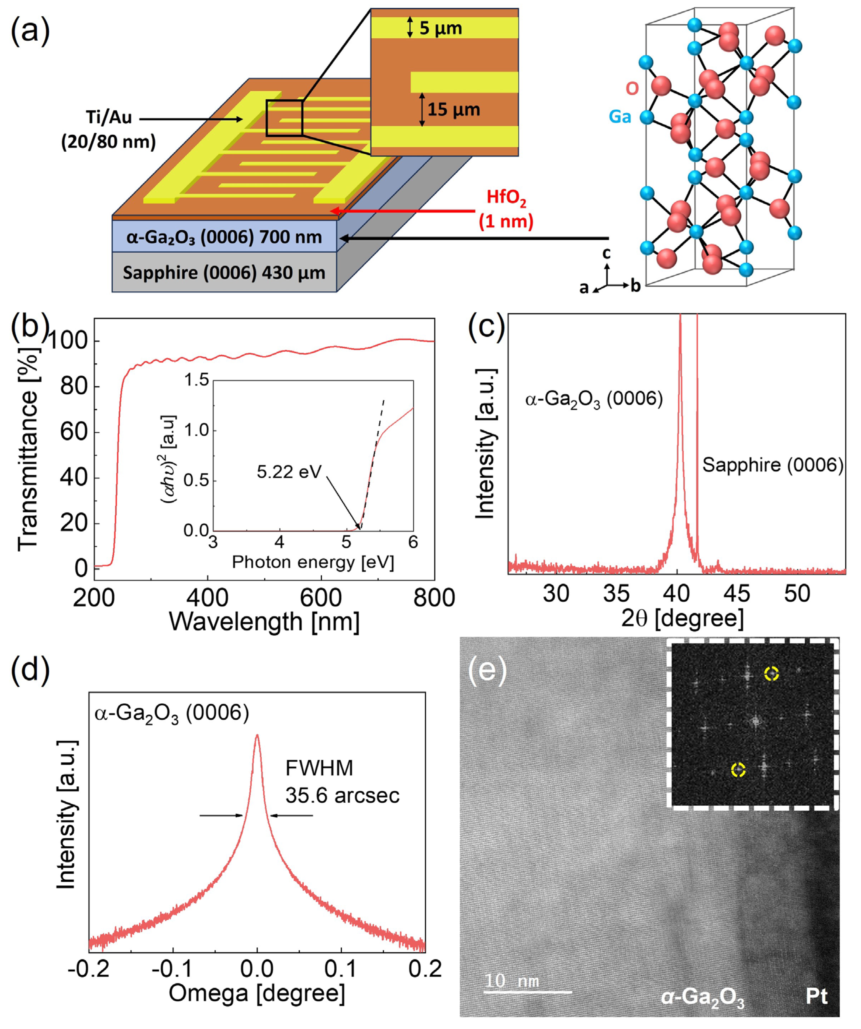
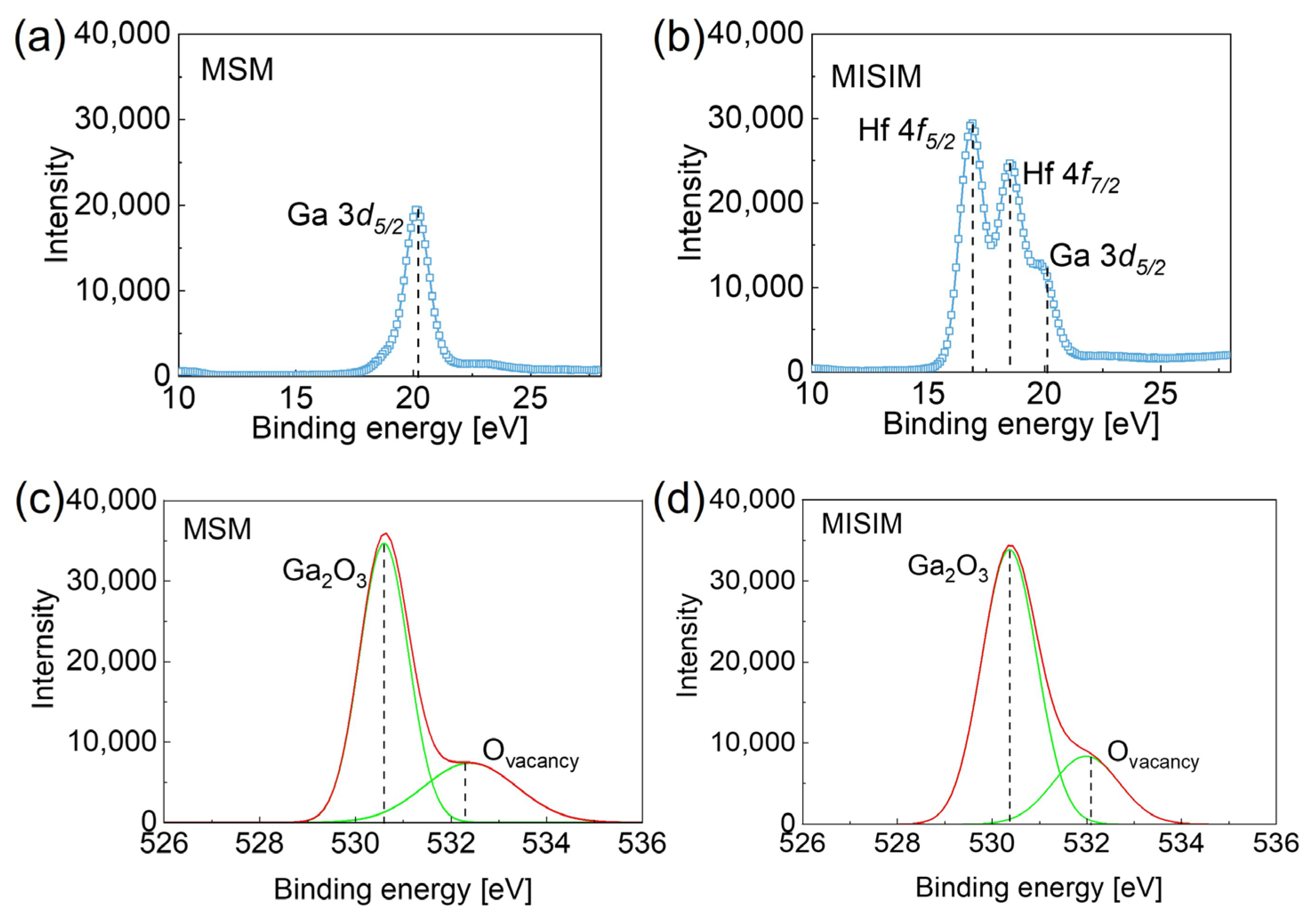
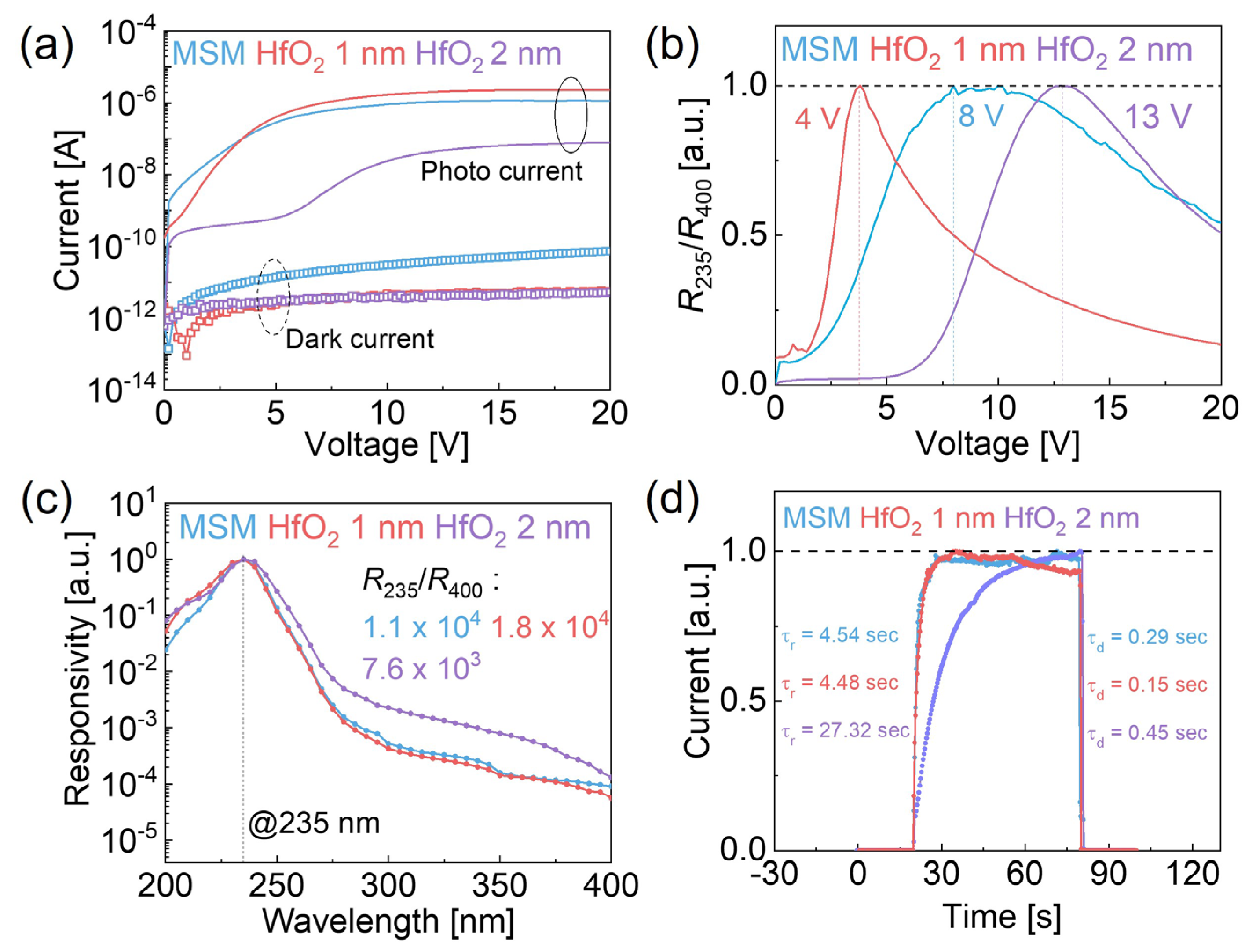
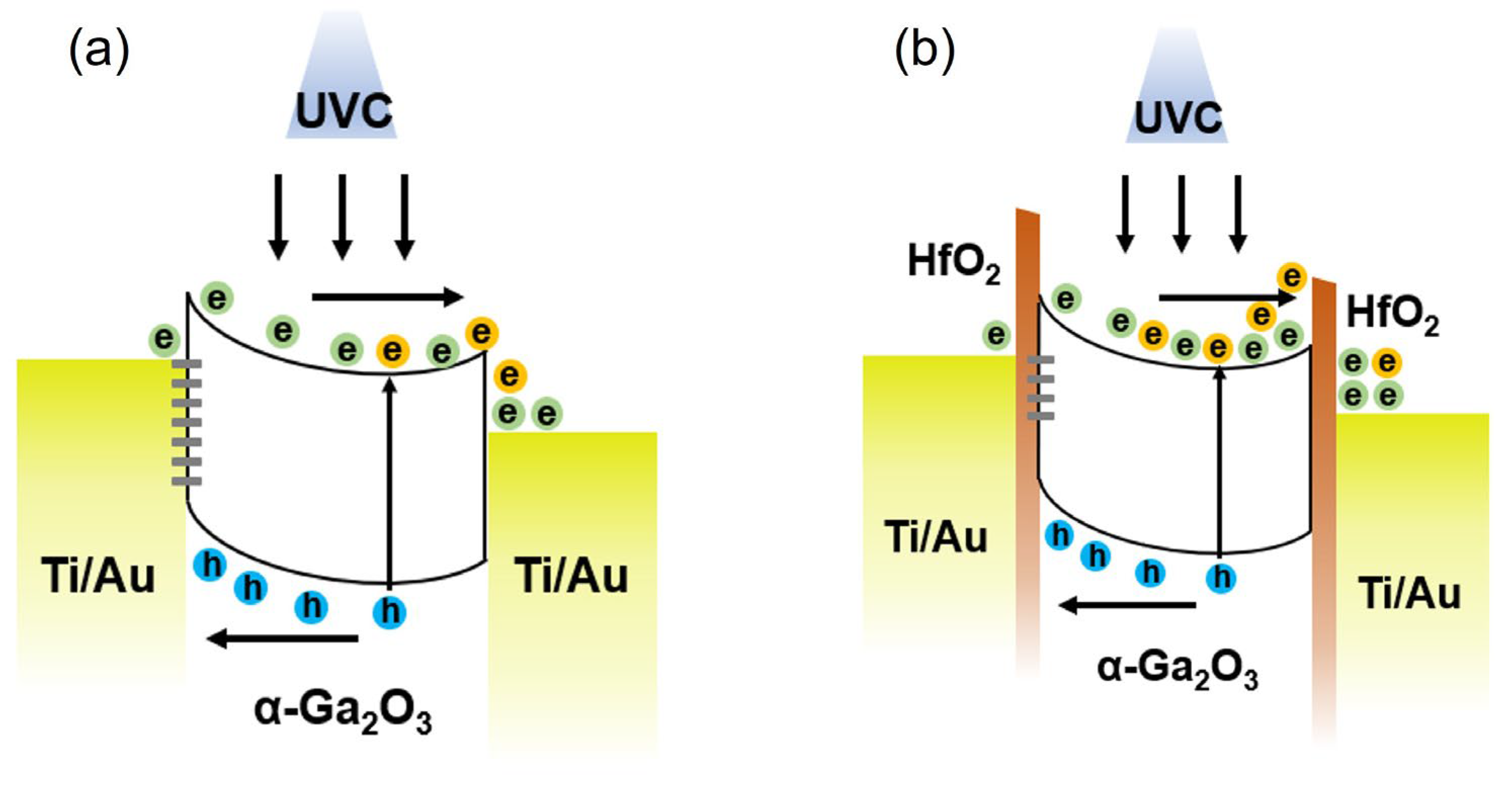
Heteroepitaxial α-Ga2O3 layers were grown on a 2-inch (0001) sapphire substrate using hydride vapor phase epitaxy (HVPE) at 470 °C, with GaCl and O2 as precursors. The undoped α-Ga2O3 films were grown to a thickness of 700 nm for 6 min. Following surface cleaning with acetone and isopropyl alcohol (IPA), HfO2 layers were deposited via atomic layer deposition (ALD) at 360 °C, using tetrakis (ethylmethylamino) hafnium (TEMAhf) as the precursor and ozone as the reactant. HfO2 thicknesses of 1 nm and 2 nm were achieved, with a growth rate of approximately 0.74 Å/cycle. Interdigitated Ti/Au (20 nm/80 nm) electrodes were then fabricated using electron-beam evaporation and a lift-off process, covering an active area of 0.5 mm2, with electrode widths of 5 μm and an interelectrode spacing of 12.5 μm. Two device configurations were prepared: a metal–insulator–semiconductor–insulator–metal (MISIM) structure with the HfO2 insulating layer and a metal–semiconductor–metal (MSM) structure without it.
For UVC illumination, a monochromator (CS 130B-1-MC, Newport Corporation, Irvine, CA, USA) paired with a xenon arc lamp (6269, Newport Corporation, USA) was used, and the wavelength-specific intensity was measured with an optical power and energy meter (2938-R, Newport Corporation, USA). Current–voltage (I–V) characteristics were assessed using a precision source/measurement unit (B2912B, Keysight, Santa Rosa, CA, USA). The crystal quality was analyzed by high-resolution X-ray diffraction (HR-XRD) on a SmartLAB system (Rigaku), and the surface chemistry was characterized via X-ray photoelectron spectroscopy (XPS) using a VersaProbe III system (ULVAC-PHI). A transmission electron microscope (TEM) was used for the crystal structure (EM-ARM200F, JEOL, Ltd., Tokyo, Japan) at 200 keV. The selected area electron diffraction (SAED) pattern was analyzed using the Gatan Digital Micrograph® software (version 3.6.0, AMETEK, Inc., Berwyn, PA, USA).

3. Results

Figure 1a illustrates a schematic of the fabricated device and a 3D schematic diagram of the α-Ga2O3 lattice structure. Figure 1b presents the optical transmittance spectrum and Tauc plot of the heteroepitaxial α-Ga2O3 layer, used to determine its optical bandgap. The results show that the α-Ga2O3 film fully absorbs light with wavelengths below 250 nm, and its optical bandgap was calculated to be approximately 5.22 eV, derived from the Tauc plot using Equation (1).
(αhν)2 = A(Eg)
This value is consistent with the previously reported bandgaps of α-Ga2O3 [18,20,22]. In addition, Figure 1c presents the XRD measurements, revealing two distinct diffraction peaks corresponding to the Al2O3 (0006) and α-Ga2O3 (0006) planes. These findings confirm that the α-Ga2O3 film grew epitaxially along the (0006) direction on the sapphire (Al2O3) substrate. In Figure 1d, the rocking curve of α-Ga2O3 exhibits a full width at half maximum (FWHM) of 35.6 arcseconds, which is consistent with previously reported values for α-Ga2O3 [22,25].
The cross-view TEM image in Figure 1e shows that α-Ga2O3 was preferentially grown in the (0006) direction along the c-axis of the sapphire substrate, consistent with the XRD results. The ideal d-spacing of α-Ga2O3 (0006) is 2.238 Å, whereas the measured d-spacing from the SAED pattern is 2.215 Å, showing evidence of compressive strain. This has been attributed to the residual stresses caused by the lattice mismatch between the sapphire substrate and heteroepitaxial α-Ga2O3 layer, which is generally observed in a heteroepitaxial growth of α-Ga2O3 on a sapphire substrate [26].
Figure 2 investigates the deposition of HfO2 via X-ray photoelectron spectroscopy (XPS) and assesses the impact of ozone supplied during atomic layer deposition (ALD) on oxygen vacancies. Figure 2a presents the Ga 3d spectrum for the MSM structure, showing a peak at a binding energy of 20.1 eV. In contrast, Figure 2b reveals additional Hf 4f peaks at 16.9 eV and 18.5 eV in the MISIM structure, confirming successful HfO2 deposition [27,28]. Figure 2c,d display the O 1s spectra, deconvoluted into two peaks at 530.6 eV (Ga-O bonds) and 532.1 eV (oxygen vacancies). The oxygen vacancy ratio, calculated from the peak areas, was 28.8% for the MSM structure and 23.1% for the MISIM structure, indicating a 5.7% reduction attributed to the oxygen vacancy treatment effect from the ozone during ALD. Oxygen vacancies are known to impair photodetector performance by increasing the dark current [29]. While oxygen annealing typically requires temperatures above 600 °C for a significant effect, the ALD process at 360 °C yielded only modest vacancy reduction [30,31].
Figure 3a presents the I–V characteristics of the α-Ga2O3 MSM and MISIM devices under dark and UVC illumination (235 nm) conditions. At 20 V, the dark currents were 73.3 pA for the MSM device, 6.61 pA for the MISIM device with 1 nm HfO2, and 5.27 pA for the 2 nm HfO2 device, indicating that HfO2 layers effectively reduce the dark current. The decrease in the dark current is attributed to suppressed electron injections due to reduced tunneling through the additional insulating HfO2 layer. Under UVC illumination at 20 V, the photocurrents were 1.14 μA (MSM), 2.3 μA (1 nm HfO2 MISIM), and 79.4 nA (2 nm HfO2 MISIM), with the 1 nm HfO2 MISIM device surpassing the MSM device. The observed enhanced photocurrent is presumably attributed to reduced trap states at the HfO2/α–Ga2O3 interface, not due to a change in Schottky barrier height. The 2 nm HfO2 MISIM device showed an unstable photocurrent below 8 V, attributed to trap states at the HfO2/Ga2O3 interface, which immobilize electrons in the Ga2O3 layer at low voltages. However, at voltages above 8 V, the traps become sufficiently filled, allowing electrons to escape under UVC illumination, resulting in an increased current [32,33]. Figure 3b compares the responsivity rejection ratio as a function of the applied voltage at wavelengths of 235 and 400 nm, highlighting the peak voltages. Figure 3c compares these wavelengths under the peak voltage, calculated using Equation (2):
R = ( I p I d ) /   P × S device
where Ip is the channel current under illumination, Id is the dark current, P is the incident light intensity, and Sdevice is the effective irradiated area. The rejection ratios (R235/R400) were 1.1 × 10⁴ (MSM), 1.8 × 10⁴ (1 nm HfO2 MISIM), and 7.6 × 10³ (2 nm HfO2 MISIM), with the 1 nm HfO2 MISIM device showing high responsivity at 235 nm and low responsivity at 400 nm, confirming enhanced UVC selectivity. Figure 3d shows the response current during UVC switching on/off at 235 nm under a bias of 20 V. The rise time (τr) and decay time (τd), defined as the time required for the current to change from 10% to 90% and from 90% to 10% of its final value, respectively, were measured for the MSM, as well as the 1 and 2 nm HfO2 MISIM devices as 4.51 s, 4.48 s, and 27.32 s for τr and 0.29 s, 0.15 s, and 0.45 s for τd, respectively. The 1 nm HfO2 MISIM device’s faster τr and τd resulted from the reduced trapping of photogenerated holes at the surface states. Conversely, the 2 nm HfO2 MISIM device’s thicker layer lowered the tunneling probability, slowing carrier transport and extending response times [34].
Figure 4a,b show the band diagrams of the MSM and MISIM structures, respectively. Typically, an insulating HfO2 layer suppresses tunneling, reducing the current, as evidenced by the lower dark currents in the MISIM devices shown in Figure 3a. However, when a 1 nm HfO2 layer is used under UVC illumination (energy exceeding the α-Ga2O3 bandgap), the MISIM device exhibits an increased photocurrent. As shown in Figure 4b, the HfO2/Ga2O3 interface in the MISIM structure has fewer traps than the Ga2O3/Ti/Au interface in the MSM structure, enhancing the photocurrent by mitigating trap-related losses. This improvement is expected to outweigh the current reduction owing to tunneling suppression [35,36]. However, increasing the HfO2 thickness to 2 nm reduces the photocurrent, as the lower tunneling probability dominates over the benefits of reduced traps. For a dark current, where no UVC energy is present, even a 1 nm HfO2 layer effectively suppresses tunneling, resulting in a significantly lower dark current in the MISIM structure compared to the MSM structure.
Figure 5a presents the I–V measurements at 300 °C. Below 8 V, the 1 nm HfO2 MISIM device exhibited a higher current than the MSM device, which is attributed to reduced interface traps and moderated tunneling suppression. Figure 5b compares the responsivity at 20 V as a function of temperature, showing an increase with temperature. This behavior can be attributed to thermal excitation, which affects both Ip and Id. However, while the increased Id is primarily attributed to thermally generated carriers, the increased Ip is ascribed not only to the thermally generated carriers but also to enhanced photoexcitation at elevated temperatures, which further facilitates the de-trapping of carriers from trap states. Consequently, more carriers become available for conduction under illumination, leading to an increased photocurrent and enhanced responsivity at an elevated temperature [37]. Figure 5c illustrates PDCR with variable temperatures for UV photodetectors based on Ga2O3 and various other materials [3,4,10,15,19,22,28,31,33,38,39,40]. Most previously reported works have included characterizations at room temperature, and characterizations at elevated temperatures are not investigated enough. Our work demonstrates insertion of the ultra-thin HfO2 interlayer-enabled high PDCR even under high-temperature conditions. Figure 5d shows the transient response at 300 °C. The τr and τd for the MSM and 1 and 2 nm MISIM devices were 0.47 s, 1.21 s, and 1.39 s and 1.16 s, 1.05 s, and 1.67 s, respectively. At 300 °C, the increased thermal energy enabled electrons in the MSM device to escape interface traps and enter the conduction band more readily, resulting in a shorter τr compared with the 1 nm HfO2 MISIM device. However, the decay times were longer than those at room temperature because of the increased persistent photoconductivity (PPC) effect. PPC refers to the phenomenon in which photoconductivity persists even after the light source has been removed. This effect is commonly observed in oxide semiconductors with oxygen vacancies and a high density of defects [3,37,41].
Table 1 summarizes the key performance metrics of Ga2O3 thin-film-based photodetectors, showing that the performance varies significantly depending on the Ga2O3 crystal phase and growth method [2,3,10,11,42,43,44]. The MISIM α-Ga2O3 device developed in this study demonstrated an enhanced photocurrent due to the reduced trap states at the HfO2/α-Ga2O3 interface and a suppressed dark current by the insulating HfO2 layer. These attributes resulted in both increased PDCR and rejection ratios that confirmed enhanced UVC selectivity. Furthermore, the use of the HVPE growth process presents strong potential for scalable production. Although further research is needed to improve film quality and device performance, this study offers a promising approach for the application of a heteroepitaxial α-Ga2O3 layer in UVC photodetectors.

4. Conclusions

In conclusion, this study investigated the impact of HfO2-layer presence and thickness on the optical and electrical performance of heteroepitaxial α-Ga2O3 layer-based UVC photodetectors. The structural and compositional characterizations of α-Ga2O3 were thoroughly analyzed using HR-XRD, XPS, TEM, and SAED. I–V measurements revealed that MISIM devices with 1 nm and 2 nm HfO2 layers achieved significantly lower dark currents than the MSM device, owing to the tunneling suppression induced by the HfO2 layer. Under 235 nm UVC illumination, the 1 nm HfO2 MISIM device delivered the highest photocurrent (2.3 μA at 20 V), driven by reduced surface traps, while the 2 nm HfO2 MISIM device showed a lower photocurrent due to increased tunneling resistance. In addition, the 1 nm HfO2 MISIM device exhibited the highest responsivity (1.8 × 10⁴ A/W), outperforming the MSM (1.1 × 10⁴ A/W) and 2 nm HfO2 MISIM (7.6 × 10³ A/W) devices, indicating enhanced UVC selectivity and a reduced UVC on/off response time. At 300 °C, the 1 nm HfO2 device exhibited a slight dark current increase from thermal-assisted tunneling but maintained superior responsivity compared to the MSM device. Overall, the 1 nm HfO2 layer optimized the photoresponse by minimizing traps and ensured robust performance at high temperatures, establishing α-Ga2O3-based MISIM photodetectors as highly effective for UVC detection in demanding environments.

Author Contributions

Conceptualization, S.Y., S.O., and G.Y.; methodology, S.Y., S.O., G.L., J.-H.P., D.-W.J., and G.Y.; formal analysis, S.Y., S.O., and G.L.; investigation, S.Y., S.O., G.L., Y.K., S.K., M.S., and G.Y.; resources, J.-H.P., D.-W.J., and G.Y.; data curation, S.Y. and S.O.; writing—original draft preparation, S.Y., and G.Y.; writing—review and editing, S.Y., and G.Y.; supervision, G.Y.; project administration, G.Y.; funding acquisition, G.Y. All authors have read and agreed to the published version of the manuscript.

Funding

This research was supported by a KEIT grant (RS-2022-00154729) funded by the Korean Government (MOTIE).

Data Availability Statement

The data presented in this study are available on request from the corresponding author.

Conflicts of Interest

The authors declare no conflicts of interest.

References

  1. Sang, L.; Liao, M.; Sumiya, M. A Comprehensive Review of Semiconductor Ultraviolet Photodetectors: From Thin Film to One-Dimensional Nanostructures. Sensors 2013, 13, 10482–10518. [Google Scholar] [CrossRef]
  2. Blumenschein, N.; Paskova, T.; Muth, J.F. Effect of Growth Pressure on PLD-Deposited Gallium Oxide Thin Films for Deep-UV Photodetectors. Phys. Status Solidi (A) Appl. Mater. Sci. 2019, 216, 1900098. [Google Scholar] [CrossRef]
  3. Tak, B.R.; Garg, M.; Dewan, S.; Torres-Castanedo, C.G.; Li, K.H.; Gupta, V.; Li, X.; Singh, R. High-Temperature Photocurrent Mechanism of β-Ga2O3 Based Metal-Semiconductor-Metal Solar-Blind Photodetectors. J. Appl. Phys. 2019, 125, 144501. [Google Scholar] [CrossRef]
  4. Wei, T.C.; Tsai, D.S.; Ravadgar, P.; Ke, J.J.; Tsai, M.L.; Lien, D.H.; Huang, C.Y.; Horng, R.H.; He, J.H. See-through Ga2O3 Solar-Blind Photodetectors for Use in Harsh Environments. IEEE J. Sel. Top. Quantum Electron. 2014, 20, 112–117. [Google Scholar] [CrossRef]
  5. Kaur, D.; Kumar, M. A Strategic Review on Gallium Oxide Based Deep-Ultraviolet Photodetectors: Recent Progress and Future Prospects. Adv. Opt. Mater. 2021, 9, 2002160. [Google Scholar] [CrossRef]
  6. Yam, J.C.S.; Kwok, A.K.H. Ultraviolet Light and Ocular Diseases. Int. Ophthalmol. 2014, 34, 383–400. [Google Scholar] [CrossRef]
  7. Narayanan, D.L.; Saladi, R.N.; Fox, J.L. Ultraviolet Radiation and Skin Cancer. Int. J. Dermatol. 2010, 49, 978–986. [Google Scholar] [CrossRef]
  8. Yang, C.; Liang, H.; Zhang, Z.; Xia, X.; Tao, P.; Chen, Y.; Zhang, H.; Shen, R.; Luo, Y.; Du, G. Self-Powered SBD Solar-Blind Photodetector Fabricated on the Single Crystal of β-Ga2O3. RSC Adv 2018, 8, 6341–6345. [Google Scholar] [CrossRef]
  9. Alema, F.; Hertog, B.; Mukhopadhyay, P.; Zhang, Y.; Mauze, A.; Osinsky, A.; Schoenfeld, W.V.; Speck, J.S.; Vogt, T. Solar Blind Schottky Photodiode Based on an MOCVD-Grown Homoepitaxial β-Ga2O3 Thin Film. APL Mater. 2019, 7, 022527. [Google Scholar] [CrossRef]
  10. Singh Pratiyush, A.; Krishnamoorthy, S.; Vishnu Solanke, S.; Xia, Z.; Muralidharan, R.; Rajan, S.; Nath, D.N. High Responsivity in Molecular Beam Epitaxy Grown β-Ga2O3 Metal Semiconductor Metal Solar Blind Deep-UV Photodetector. Appl. Phys. Lett. 2017, 110, 221107. [Google Scholar] [CrossRef]
  11. Li, Z.; An, Z.; Xu, Y.; Cheng, Y.; Cheng, Y.; Chen, D.; Feng, Q.; Xu, S.; Zhang, J.; Zhang, C.; et al. Improving the Production of High-Performance Solar-Blind β-Ga2O3 Photodetectors by Controlling the Growth Pressure. J. Mater. Sci. 2019, 54, 10335–10345. [Google Scholar] [CrossRef]
  12. Chu, S.Y.; Shen, M.X.; Yeh, T.H.; Chen, C.H.; Lee, C.T.; Lee, H.Y. Investigation of Ga2O3-Based Deep Ultraviolet Photodetectors Using Plasma-Enhanced Atomic Layer Deposition System. Sensors 2020, 20, 6159. [Google Scholar] [CrossRef]
  13. Pearton, S.J.; Yang, J.; Cary, P.H.; Ren, F.; Kim, J.; Tadjer, M.J.; Mastro, M.A. A Review of Ga2O3 Materials, Processing, and Devices. Appl. Phys. Rev. 2018, 5, 011301. [Google Scholar] [CrossRef]
  14. Liu, Z.; Tang, W. A Review of Ga2O3 Deep-Ultraviolet Metal-Semiconductor Schottky Photodiodes. J. Phys. D Appl. Phys. 2023, 56, 093002. [Google Scholar] [CrossRef]
  15. Zhang, W.; Wang, W.; Zhang, J.; Zhang, T.; Chen, L.; Wang, L.; Zhang, Y.; Cao, Y.; Ji, L.; Ye, J. Directional Carrier Transport in Micrometer-Thick Gallium Oxide Films for High-Performance Deep-Ultraviolet Photodetection. ACS Appl. Mater. Interfaces 2023, 15, 10868–10876. [Google Scholar] [CrossRef] [PubMed]
  16. Sheoran, H.; Fang, S.; Liang, F.; Huang, Z.; Kaushik, S.; Manikanthababu, N.; Zhao, X.; Sun, H.; Singh, R.; Long, S. High Performance of Zero-Power-Consumption MOCVD-Grown β-Ga2O3-Based Solar-Blind Photodetectors with Ultralow Dark Current and High-Temperature Functionalities. ACS Appl. Mater. Interfaces 2022, 14, 52096–52107. [Google Scholar] [CrossRef] [PubMed]
  17. Muazzam, U.U.; Chavan, P.; Raghavan, S.; Muralidharan, R.; Nath, D.N. Optical Properties of Mist CVD Grown α-Ga2O3. IEEE Photonics Technol. Lett. 2020, 32, 422–425. [Google Scholar] [CrossRef]
  18. Son, H.; Choi, Y.-J.; Hwang, J.; Jeon, D.-W. Influence of Post-Annealing on Properties of α-Ga2O3 Epilayer Grown by Halide Vapor Phase Epitaxy. ECS J. Solid State Sci. Technol. 2019, 8, Q3024–Q3027. [Google Scholar] [CrossRef]
  19. Bae, J.; Park, J.H.; Jeon, D.W.; Kim, J. Self-Powered Solar-Blind α-Ga2O3 Thin-Film UV-C Photodiode Grown by Halide Vapor-Phase Epitaxy. APL Mater. 2021, 9, 101108. [Google Scholar] [CrossRef]
  20. Leach, J.H.; Udwary, K.; Rumsey, J.; Dodson, G.; Splawn, H.; Evans, K.R. Halide Vapor Phase Epitaxial Growth of β-Ga2O3 and α-Ga2O3 Films. APL Mater. 2019, 7, 022504. [Google Scholar] [CrossRef]
  21. Lee, M.; Yang, M.; Lee, H.Y.; Lee, H.U.; Lee, H.; Son, H.; Kim, U.J. The Growth of HVPE α-Ga2O3 Crystals and Its Solar-Blind UV Photodetector Applications. Mater. Sci. Semicond. Process. 2021, 123, 105565. [Google Scholar] [CrossRef]
  22. Kim, S.; Yoon, Y.; Seo, D.; Park, J.H.; Jeon, D.W.; Hwang, W.S.; Shin, M. Alpha-Phase Gallium Oxide-Based UVC Photodetector with High Sensitivity and Visible Blindness. APL Mater. 2023, 11, 061107. [Google Scholar] [CrossRef]
  23. Oshima, T.; Okuno, T.; Arai, N.; Suzuki, N.; Hino, H.; Fujita, S. Flame Detection by a β-Ga2O3-Based Sensor. Jpn. J. Appl. Phys. 2009, 48, 011605. [Google Scholar] [CrossRef]
  24. Kaneko, K.; Fujita, S.; Shinohe, T.; Tanaka, K. Progress in α-Ga2O3 for Practical Device Applications. Jpn. J. Appl. Phys. 2023, 62, SF0803. [Google Scholar] [CrossRef]
  25. Kim, S.; Kim, H.W.; Kim, H.Y.; Jeon, D.W.; Cho, S.B.; Park, J.H. A Pre-Reaction Suppressing Strategy for α-Ga2O3 Halide Vapor Pressure Epitaxy Using Asymmetric Precursor Gas Flow. CrystEngComm 2022, 24, 3049–3056. [Google Scholar] [CrossRef]
  26. Son, H.; Choi, Y.; Hong, S.-K.; Park, J.-H.; Jeon, D.-W. Reduction of dislocations in α-Ga2O3 epilayers grown by halide vapor-phase epitaxy on a conical frustum-patterned sapphire substrate. IUCrJ 2021, 8, 462–467. [Google Scholar] [CrossRef]
  27. Feng, Z.; Feng, Q.; Zhang, J.; Zhang, C.; Zhou, H.; Li, X.; Huang, L.; Xu, L.; Hu, Y.; Zhao, S.; et al. Band Alignments of SiO2 and HfO2 Dielectrics with (AlxGa1-x)2O3 Film (0≤x≤0.53) Grown on Ga2O3 Buffer Layer on Sapphire. J. Alloys Compd. 2018, 745, 292–298. [Google Scholar] [CrossRef]
  28. Barreca, D.; Milanov, A.; Fischer, R.A.; Devi, A.; Tondello, E. Hafnium Oxide Thin Film Grown by ALD: An XPS Study. Surf. Sci. Spectra 2007, 14, 34–40. [Google Scholar] [CrossRef]
  29. Wang, J.; Ji, X.; Yan, Z.; Qi, S.; Liu, X.; Zhong, A.; Li, P. The Role of oxygen vacancies in Ga2O3-Based Solar-Blind Photodetectors. J. Alloys Compd. 2024, 970, 172448. [Google Scholar] [CrossRef]
  30. Wang, H.; Tang, C.; Yang, W.; Zhao, J.; Liu, L.; Mu, J.; Zhang, Y.; Zeng, C. Recrystallization Behavior, Oxygen Vacancy and Photoluminescence Performance of Sputter-Deposited Ga2O3 Films via High-Vacuum in Situ Annealing. Ceram. Int. 2022, 48, 3481–3488. [Google Scholar] [CrossRef]
  31. Yuan, L.; Li, S.; Song, G.; Sun, X.W.; Zhang, X. Solution-Processed Amorphous Gallium Oxide Gate Dielectric for Low-Voltage Operation Oxide Thin Film Transistors. J. Mater. Sci. Mater. Electron. 2021, 32, 8347–8353. [Google Scholar] [CrossRef]
  32. Seol, J.H.; Kang, S.B.; Lee, C.J.; Won, C.H.; Park, H.; Lee, J.H.; Hahm, S.H. Graphene/Al2O3/AlGaN/GaN Schottky MISIM Diode for Sensing Double UV Bands. IEEE Sens. J. 2016, 16, 6903–6907. [Google Scholar] [CrossRef]
  33. Chang, C.Y.; Huang, Y.W.; Lin, Y.J.; Liao, J.Y.; Lin, J.S.; Li, Y.M.; Chen, C.Y.; Sheu, J.T.; Pan, F.M. Photoconductive Properties of Polycrystalline Selenium Based Lateral MISIM Photodetectors of High Quantum Efficiency Using Different Dielectrics as the Charge Blocking Layer. J. Mater. Sci. Mater. Electron. 2019, 30, 12956–12965. [Google Scholar] [CrossRef]
  34. Zhang, C.; Tian, C.; Wei, S.; Cai, Z.; Long, H.; Zhang, J.; Hong, R.; Yang, W. High-Performance β-GaO MISIM Solar-Blind Photodetectors With an Interfacial AlN Layer. IEEE Photonics Technol. Lett. 2024, 36, 593–596. [Google Scholar] [CrossRef]
  35. Bhattacharyya, A.; Ranga, P.; Saleh, M.; Roy, S.; Scarpulla, M.A.; Lynn, K.G.; Krishnamoorthy, S. Schottky Barrier Height Engineering in β-Ga2O3 Using SiO2 Interlayer Dielectric. IEEE J. Electron Devices Soc. 2020, 8, 286–294. [Google Scholar] [CrossRef]
  36. Song, S.; Kim, S.H.; Kim, S.G.; Han, K.H.; Kim, H.J.; Yu, H.Y. Effective Schottky Barrier Height and Interface Trap Density Reduction Engineering Using 2-Dimensional Reduced Graphene Oxide Interlayer for Metal-Interlayer-Semiconductor Contact Structure. J. Alloys Compd. 2023, 937, 168327. [Google Scholar] [CrossRef]
  37. Di Bartolomeo, A.; Kumar, A.; Durante, O.; Sessa, A.; Faella, E.; Viscardi, L.; Intonti, K.; Giubileo, F.; Martucciello, N.; Romano, P.; et al. Temperature-dependent photoconductivity in two-dimensional MoS2 transistors. Mater. Today Nano 2023, 24, 100382. [Google Scholar] [CrossRef]
  38. Qiu, M.; Jia, Z.; Yang, M.; Nishimura, K.; Lin, C.-T.; Jiang, N.; Yuan, Q. High Detectivity Solar Blind Photodetector Based on Mechanical Exfoliated Hexagonal Boron Nitride Films. Nanotechnology 2023, 34, 285204. [Google Scholar] [CrossRef]
  39. Sang, L.W.; Liao, M.Y.; Koide, Y.; Sumiya, M. High-temperature ultraviolet detection based on InGaN Schottky photodiodes. Appl. Phys. Lett. 2011, 99, 031115:1–031115:3. [Google Scholar] [CrossRef]
  40. Khan, T.; Kandar, S.; Ali, S.; Singh, P.; Horng, R.-H.; Singh, R. Selective UV Sensing for Energy-Efficient UV-A Artificial Synapses Using a ZnO/ZnGa2O4 Heterojunction Diode. Small 2025, 21, 2500098. [Google Scholar] [CrossRef]
  41. Yang, H.; Cheng, T.-H.; Xin, Q.; Liu, Y.; Feng, H.Y.; Luo, F.; Mu, W.; Jia, Z.; Tao, X. Efficient Suppression of Persistent Photoconductivity in β-Ga2O3-Based Photodetectors with Square Nanopore Arrays. ACS Appl. Mater. Interfaces 2023, 15, 32522–32532. [Google Scholar] [CrossRef]
  42. Sui, Y.; Liang, H.; Huo, W.; Zhan, X.; Zhu, T.; Mei, Z. Flexible UV Detectors Based on In-Situ Hydrogen Doped Amorphous Ga2O3 with High Photo-to-Dark Current Ratio. Mater. Futures 2024, 3, 015701. [Google Scholar] [CrossRef]
  43. Wang, Z.; Huang, H.; Hou, X.; Han, K.; Zhong, W.; Feng, X.; Zhan, H.; Liu, W.; Zhao, X.; Gao, N.; et al. Crystal-Phase Engineering of ε-Ga2O3 for High-Performance Deep UV Photodetectors via MOCVD. Sci. China Mater. 2025, 68, 1174–1183. [Google Scholar] [CrossRef]
  44. Fei, Z.; Chen, Z.; Chen, W.; Chen, S.; Wu, Z.; Lu, X.; Wang, G.; Liang, J.; Pei, Y. ε-Ga2O3 thin films grown by metal-organic chemical vapor deposition and its application as solar-blind photodetectors. J. Alloys Compd. 2022, 925, 166632. [Google Scholar] [CrossRef]
Figure 1. (a) Schematic of the MISIM photodetector, featuring an HfO2 insulating layer on α-Ga2O3 and a 3D schematic diagram of the α-Ga2O3 lattice structure. (b) Optical transmittance spectrum with an inset showing the optical bandgap of the heteroepitaxial α-Ga2O3 layer, estimated using a Tauc plot. (c) High-resolution X-ray diffraction (HR-XRD) 2θ scan of the heteroepitaxial α-Ga2O3 layer. (d) HR-XRD rocking curve for the (0006) diffraction peak. (e) Cross-view transmission electron microscope (TEM) image of α-Ga2O3 thin film with an inset selected area electron diffraction pattern.
Micromachines 16 00836 g001
Figure 2. (a) XPS spectrum of Ga 3d5/2 for the MSM structure; (b) XPS spectra of Hf 4f5/2, Hf 4f7/2, and Ga 3d5/2 for the MISIM structure. The O 1s XPS spectrum (c) for the MSM structure and (d) for the MISIM structure, showing Ga2O3 and oxygen vacancies.
Micromachines 16 00836 g002
Figure 3. (a) Dark current and photocurrent under 235 nm UVC illumination for MSM and MISIM devices with 1 nm and 2 nm HfO2 layers. (b) Responsivity rejection ratio (R235/R400) as a function of voltage. (c) Responsivity as a function of wavelength at the peak voltage. (d) Response speed during UVC on/off switching at 235 nm for MSM, 1 nm HfO2 MISIM, and 2 nm HfO2 MISIM devices.
Micromachines 16 00836 g003
Figure 4. Energy band diagrams of heteroepitaxial α-Ga2O3 layer-based UVC photodetectors: (a) MSM structure and (b) MISIM structure.
Micromachines 16 00836 g004
Figure 5. (a) Photocurrent and dark current at 300 °C for MSM and MISIM devices with 1 nm and 2 nm HfO2 layers. (b) Responsivity at 20 V as a function of temperature; (c) benchmark plot of PDCR for variable high temperatures [3,4,10,15,19,22,28,31,33,38,39,40]; (d) response speed during UVC on/off switching at 235 nm and 300 °C for the MSM, 1 nm HfO2, and 2 nm HfO2 devices.
Micromachines 16 00836 g005
Table 1. Performance comparison of photodetectors fabricated on Ga2O3 thin films.
PhaseGrownDetectionPDCRResponsivityDark CurrentRef
AlphaHVPE235 nm8.7 × 103
(@20 V)
1.38 A/W
(@8 V)
73 pA
(@20 V)
This work
(w/o)
AlphaHVPE235 nm7.3 × 104
(@20 V)
0.68 A/W
(@4 V)
5.5 pA
(@20 V)
This work
(1 nm)
AlphaHVPE235 nm5.2 × 102
(@20 V)
0.17 A/W
(@13 V)
5.2 pA
(@20 V)
This work
(2 nm)
BetaPLD254 nm14
(@10 V)
30.45 A/W
(@10 V)
4.2 nA[2]
BetaPLD255 nm7.1 × 103
(@10 V)
0.74 A/W
(@10 V)
0.32 nA[3]
BetaMBE236 nm103
(@20 V)
1.5 A/W
(@4 V)
4 nA
(@20 V)
[10]
BetaRF sputtering254 nm105303 A/W10 pA
(@20 V)
[11]
AmorphousSputtering254 nm2.6 × 107
(@5 V)
3.2 × 10⁴ A/W
(@ 5V)
51 pA
(@5 V)
[42]
EpsilonMOCVD254 nm2.4 × 107639 A/W
(@10 V)
4.6 pA[43]
EpsilonMOCVD252 nm1.0 × 103
(@15 V)
0.38 A/W
(@15 V)
20 nA
(@15 V)
[44]
Disclaimer/Publisher’s Note: The statements, opinions and data contained in all publications are solely those of the individual author(s) and contributor(s) and not of MDPI and/or the editor(s). MDPI and/or the editor(s) disclaim responsibility for any injury to people or property resulting from any ideas, methods, instructions or products referred to in the content.

