Article

Improvement of AlGaN/GaN High-Electron-Mobility Transistor Radio Frequency Performance Using Ohmic Etching Patterns for Ka-Band Applications

1
International College of Semiconductor Technology, National Yang Ming Chiao Tung University (NYCU), Hsinchu City 30010, Taiwan
2
Department of Electronics and Computer Technology, University of Granada, 18014 Granada, Spain
3
Institute of Microengineering and Nanoelectronics, University Kebangsaan Malaysia, Bangi 43600, Malaysia
*
Author to whom correspondence should be addressed.
Micromachines 2024, 15(1), 81; https://doi.org/10.3390/mi15010081
Submission received: 30 November 2023 / Revised: 25 December 2023 / Accepted: 28 December 2023 / Published: 30 December 2023
(This article belongs to the Special Issue III-V Optoelectronics and Semiconductor Process Technology)

Abstract

:
In this paper, AlGaN/GaN high-electron-mobility transistors (HEMTs) with ohmic etching patterns (OEPs) “fabricated to improve device radio frequency (RF) performance for Ka-band applications” are reported. The fabricated AlGaN/GaN HEMTs with OEP structures were used to reduce the source and drain resistances (Rs and Rd) for RF performance improvements. Within the proposed study using 1 μm hole, 3 μm hole, 1 μm line, and 3 μm line OEP HEMTs with 2 × 25 μm gate widths, the small signal performance, large signal performance, and minimum noise figure (NFmin) with optimized values were measured for 1 μm line OEP HEMTs. The cut-off frequency (fT) and maximum oscillation frequency (fmax) value of the 1 μm line OEP device exhibited optimized values of 36.4 GHz and 158.29 GHz, respectively. The load–pull results show that the 1 μm line OEP HEMTs exhibited an optimized maximum output power density (Pout, max) of 1.94 W/mm at 28 GHz. The 1 μm line OEP HEMTs also exhibited an optimized NFmin of 1.75 dB at 28 GHz. The increase in the contact area between the ohmic metal and the AlGaN barrier layer was used to reduce the contact resistance of the OEP HEMTs, and the results show that the 1 μm line OEP HEMT could be fabricated, producing the best improvement in RF performance for Ka-band applications.

1. Introduction

With the growth of the Internet of Things (IoTs), artificial intelligence (AI), and the increasing demand for high-speed consumer electronics such as smart phones, smart homes, and unmanned aerial vehicles (UAV), lower-frequency system bandwidths for data transmission have become congested [1,2,3,4]. As a result, Ka-band systems have emerged in fifth-generation (5G) and beyond 5G (B5G) systems to increase spectrum allocations and data rates, and to reduce antenna sizes [5]. Power amplifiers (PAs) and low noise amplifiers (LNAs) in wireless communication circuits and their transistors are especially crucial when it comes to enhancing efficiency, gaining flatness, and lowering noise over a wide-frequency band [6]. Silicon-based transistors, such as complementary metal–oxide semiconductor field-effect transistors (CMOS FETs), can be used in radio frequency (RF) transceiver circuits given their low costs and high yield, but they suffer from low power gain, a short channel effect, and saturation effects due to scaling [7,8]. III–V-based transistors, such as AlGaAs/GaAs and AlGaN/GaN high-electron-mobility transistors (HEMTs), are also used in high-frequency PAs and LNAs, but GaAs-based HEMTs suffer from low voltage operation, low power per unit, and low power efficiency due to the small energy bandgap and low breakdown voltage [9,10,11]. On the other hand, GaN-based HEMTs have demonstrated stronger frequency response, higher power-added efficiency (PAE), and better power performance, so are suitable for 5G and B5G systems, ranging from sub-6 GHz to Ka band, due to the high breakdown voltage, high saturation current, and low-frequency noise characteristics [12,13,14,15,16,17].
Nevertheless, parasitic resistance builds up at ultra-high frequencies for GaN HEMTs due to their high operation voltages, which reduces the overall device performance, such as current density, RF power, and PAE. Solutions have been proposed to reduce the parasitic influences of GaN-based HEMTs through barrier layer recessing, ohmic regrowth, and n-type doping to lower the source and drain resistances (Rs and Rd) for direct current (DC) characteristic improvements [18,19]. In advance, researchers have reported simulated and experimental results regarding contact resistivity improvements using several ohmic recessing patterns to increase the current paths and device saturation current density [20,21,22,23,24,25,26,27].
This study further compared the DC, RF small signal, RF large signal, and RF noise performance of different ohmic etching patterns (OEPs) for Ka-band applications and to design an optimized OEP structure with lower source and drain resistances, higher saturation current density, better RF power performance, and a lower high-frequency noise. The optimized OEP device with a 1 μm line pattern demonstrated the lowest contact resistance, highest small signal and large signal performance, and the smallest minimum noise figure (NFmin) at the Ka band among the four OEP structures designed in this study.

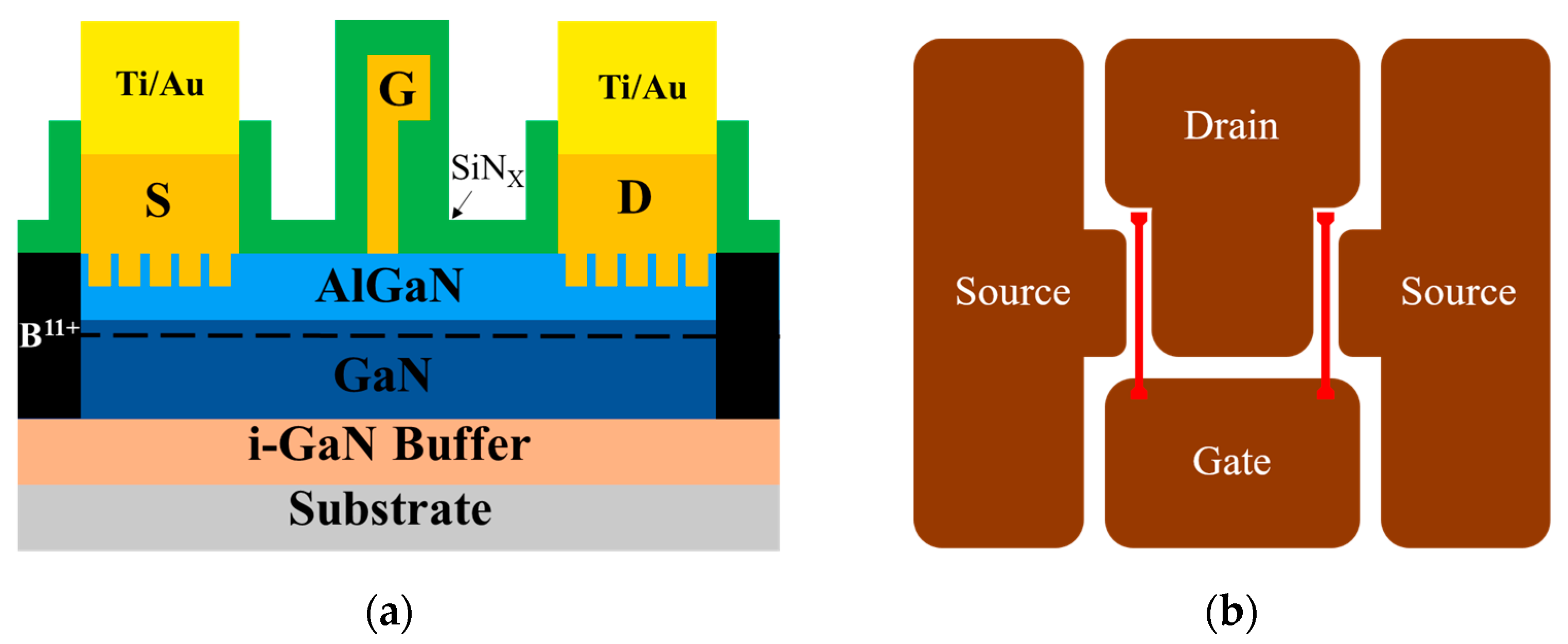
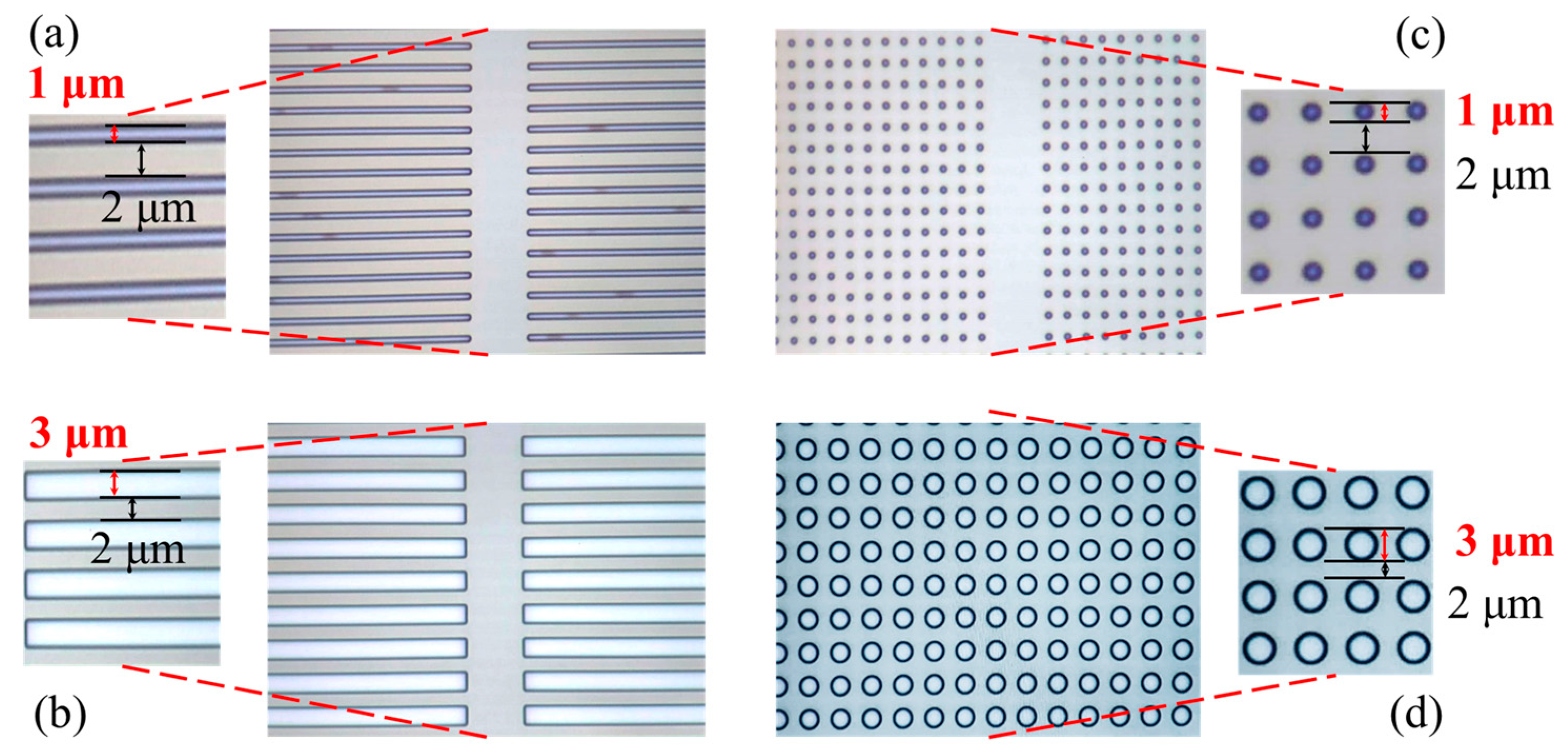
2. Materials and Methods

The AlGaN/GaN HEMTs were fabricated on a 4 inch GaN on SiC substrate. The epitaxial wafer was grown with a metal–organic chemical vapor deposition (MOCVD) system and consisted of an i-GaN buffer layer, a 0.9 μm unintentionally doped GaN channel layer, a 25 nm Al0.25Ga0.75N barrier layer, and a 2 nm GaN cap layer, as shown in Figure 1a. The device structure consisted of two gate fingers (red), one gate pad, two source pads, and one drain pad, as shown in Figure 1b. The epitaxial wafer was measured via Hall measurement at room temperature and showed an electron mobility of 1500 cm2/V·s, a sheet resistance of 280 Ω/sq, and a sheet carrier density of 1 × 10¹³/cm2.
Alignment marks were fabricated first on the epitaxial wafer during the OEP process. Four different OEPs of 1 μm lines, 3 μm lines, 1 μm holes, and 3 μm holes, respectively, were then defined and transferred to the wafer by the stepper photolithography system (stepper) [12]. There are two shapes among the four OEPs, the line patterns and the hole patterns. The defined line patterns are parallel to the current flow and have widths of 1 μm or 3 μm, with lengths equal to the source and drain active area, and separations of 2 μm between the pattern edges. The defined hole patterns have diameters of 1 μm or 3 μm, for the 1 μm holes and 3 μm holes, respectively, and the hole patterns are distributed uniformly over the source and drain active area with a 2 μm separation between the pattern edges. The optical micrographs of the developed OEP structures on the epitaxial wafer with 1 μm lines, 3 μm lines, 1 μm holes, and 3 μm holes are shown in Figure 2a,b,c,d, respectively. The schematic position of the OEP structures are shown in Figure 1a with the hole pattern rather than the line pattern for clarity.
To form OEPs at the source and drain the ohmic contact area, the inductively coupled plasma-reactive ion etching (ICP-RIE) system is then used to dry etch the GaN cap layer and the AlGaN barrier layer with Cl2/BCl3 plasma. The OEPs were etched to around 10 nm above the 2-dimensional-electron-gas (2DEG) channel, which etch-stopped at the AlGaN barrier layer. The recessed depths were chosen only above 2DEG, due to the higher contact resistances measured for the devices with recessed depth below 2DEG, as shown in previous research [28]. After wafer cleaning with a diluted hydrochloric acid (HCl) solution to remove the native oxide layer [29], an ohmic metal stack of Ti/Al/Ni/Au was deposited with the e-beam evaporation system (E-gun) and annealed by the rapid thermal annealing system (RTA) at 850 °C for 30 s in N2 ambient. The RTA process was followed by the B11+ ion implantation to define the active region of the devices. After the gate length (Lg) definition of 0.15 μm by the stepper using the 2-step photolithography process [12], the wafer was also uniformly dipped in a diluted HCl solution to remove native oxide layers before gate metal deposition [29]. Ni/Au was then deposited as the gate metal stack for Schottky contact formation and a 100 nm SiNX passivation layer was deposited using the plasma enhanced chemical vapor deposition (PECVD) for moisture protection [30]. After via-opening of the SiNX layer on the contact metal pads with the ICP system, thick metallization of a 2 μm Ti/Au metal stack was deposited using an E-gun after a wafer cleaning process using diluted HCl solution.

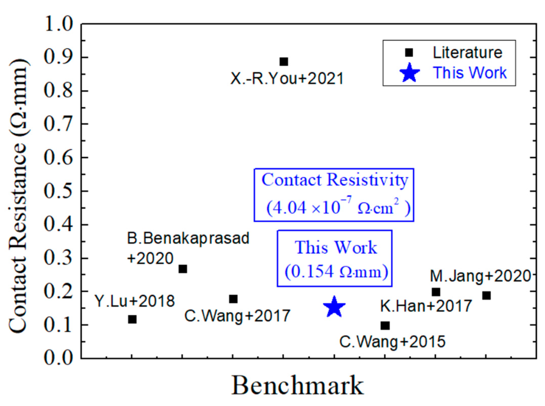
3. Results and Discussion

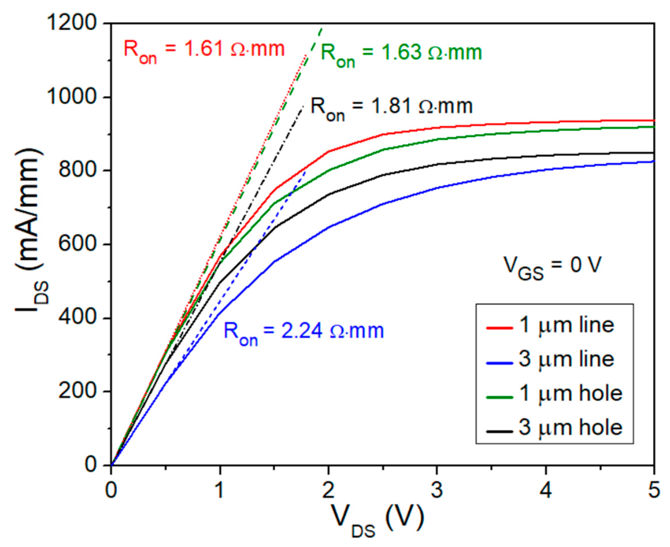
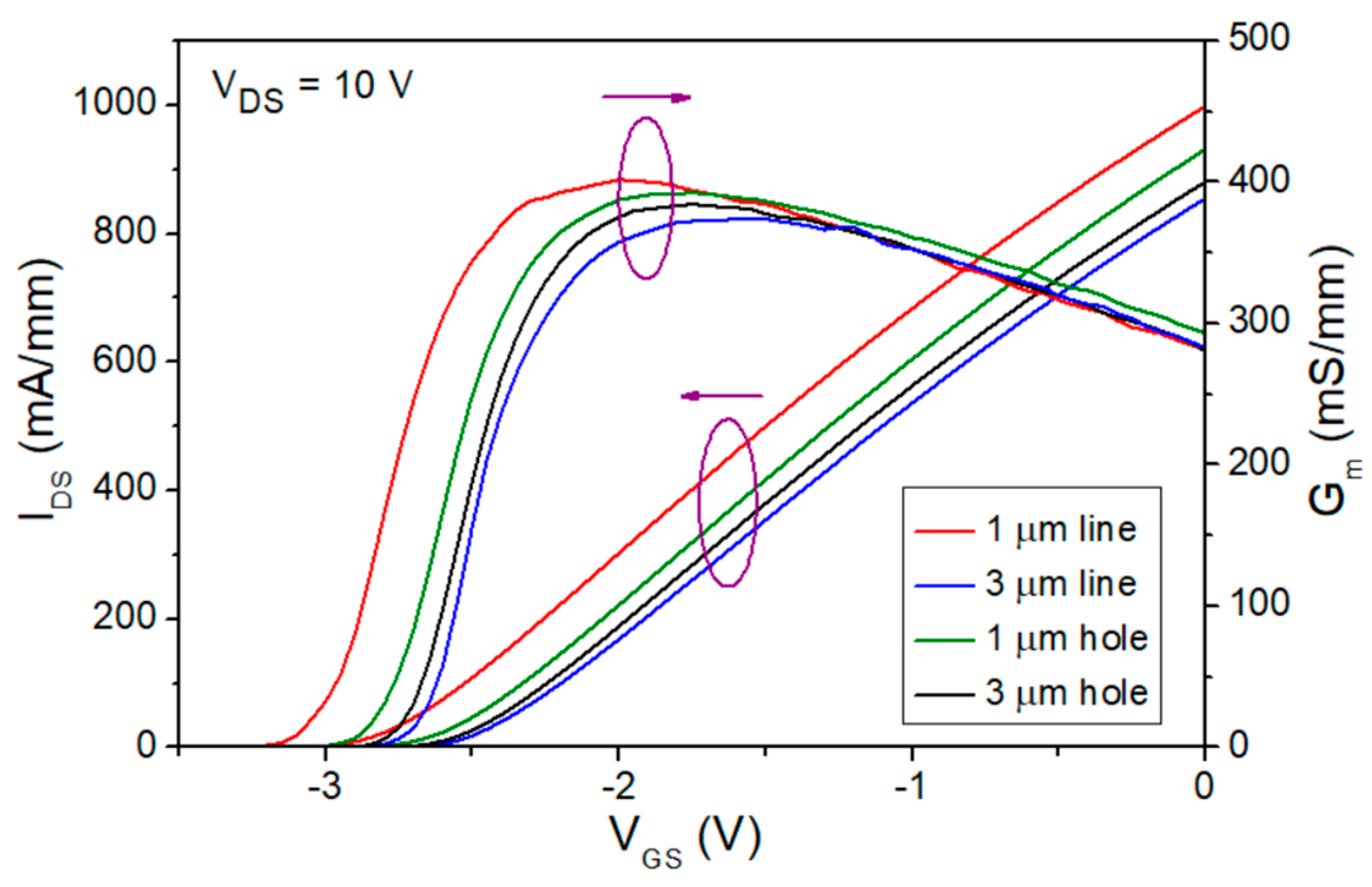
3.1. DC Characteristics

Transmission line modeling (TLM) was used in this study to determine the specific contact resistivity (ρc) and the contact resistance (Rc) of the epitaxial wafer with the four designed OEP structures and the results are shown in Table 1 [25,26].
The ρc has been improved from 2.73 × 10⁻⁶ Ω·cm2 to 4.04 × 10⁻⁷ Ω·cm2 and the Rc has been improved from 0.429 Ω·mm to 0.154 Ω·mm applying the 1 μm line OEP structure, which is the lowest value among the fabricated TLM structures with the four designed OEPs.
AlGaN/GaN HEMTs with the four designed OEPs were also fabricated on the same epitaxial wafer. The IDS−VGS and Gm−VGS curves for the four fabricated OEP AlGaN/GaN HEMTs are shown in Figure 3. The gate width and source-to-drain spacing (LSD) for the OEP GaN HEMTs are 2 × 25 μm and 2 μm, respectively. The gate-to-drain spacing (LGD) of 1.25 μm, and a gate-to-source spacing (LGS) of 0.6 μm were designed for the devices. The peak extrinsic transconductance (Gm, peak) of 403 mS/mm and the drain-to-source saturation current (IDSS) of 999 mA/mm were measured from the OEP GaN HEMT with the 1 μm line patterns at VDS = 10 V, which both demonstrated the highest value among the four OEP HEMTs, as shown in Table 2. The IDSS is defined as the drain-to-source current (IDS) when the gate-to-source voltage (VGS) equals zero and the Gm, peak is defined as the peak extrinsic transconductance value of the device with a VGS swept from −4 V to 0 V.
The IDS−VDS curves of the four OEP HEMTs with VGS equals to 0 V and VDS sweeping from 0 V to 5 V and their on-resistance (Ron) values were also measured and calculated, respectively, as shown in Figure 4 and Table 2. The HEMT devices with the 1 μm line OEP structure has the Ron of 1.61 Ω·mm, which shows the lowest Ron among the four designed OEP HEMTs.
The measured DC characteristics of the four OEP HEMTs shown in Figure 3, Figure 4, Table 1, and Table 2 exhibit improvements in the device performance. The improvement of ρc from 2.73 × 10⁻⁶ Ω·cm2 to 4.04 × 10⁻⁷ Ω·cm2 and the improvement of Rc from 0.429 Ω·mm to 0.154 Ω·mm using the 1 μm line OEP structure is attributed to the increase of contact area at the interface between the ohmic metal stack and the semiconductor layer, forming more TiNX layers and nitride vacancies, the inclusion of fringing effects, and the removal of irregular surface oxide layers [20,23,31]. Moreover, the increase in electron tunneling effect at the interface under the ohmic metal stack also stands a crucial role in the improvement of the ρc and Rc values and could be explained by the increase in N vacancies, increasing donor doping concentration and electric field, and thus increasing tunneling current [23]. A benchmark has been made to compare the lowest Rc in this work with well-known publications that also fabricated OEP GaN-based HEMTs, demonstrating the low Rc of the designed OEP HEMT in this study, as shown in Figure 5.
The trend of the Gm, peak and IDSS are also analyzed for the four OEP HEMTs, showing that 1 μm line OEP HEMTs exhibit the highest values among the four designed structures, followed by the OEP HEMTs with the 1 μm holes, the 3 μm holes, and the 3 μm lines, in descending sequence. This is attributed to the larger contact area at the interface of the 1 μm line OEP HEMTs and that the 1 μm line OEP HEMTs still obtain enough AlGaN barrier layer to form enough 2DEG. Ron values of the four designed OEP HEMTs were also analyzed and demonstrated a similar trend to that of the IDSS value. The trend of the Ron improvement for OEP HEMTs compared to non-OEP HEMTs was also found in previous research [32].

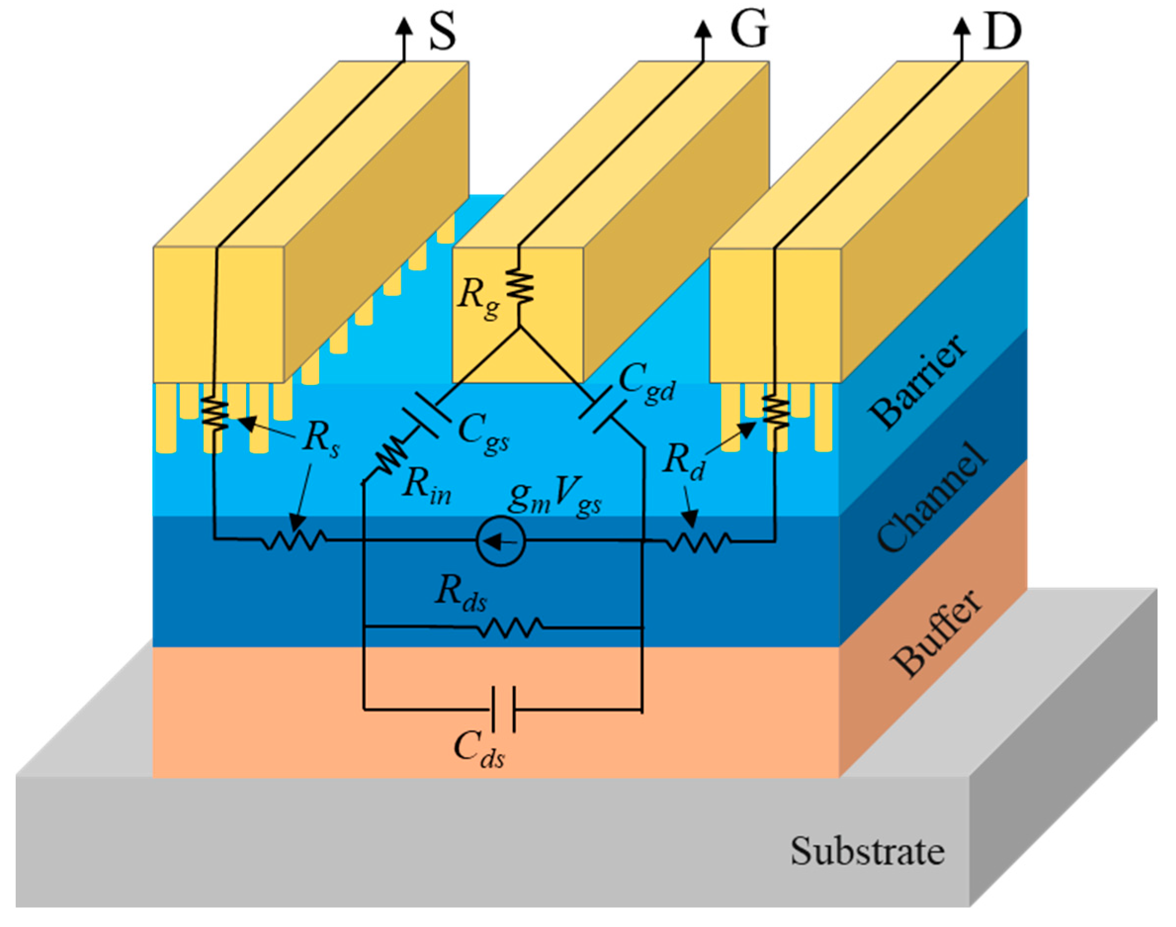
3.2. RF Characteristics

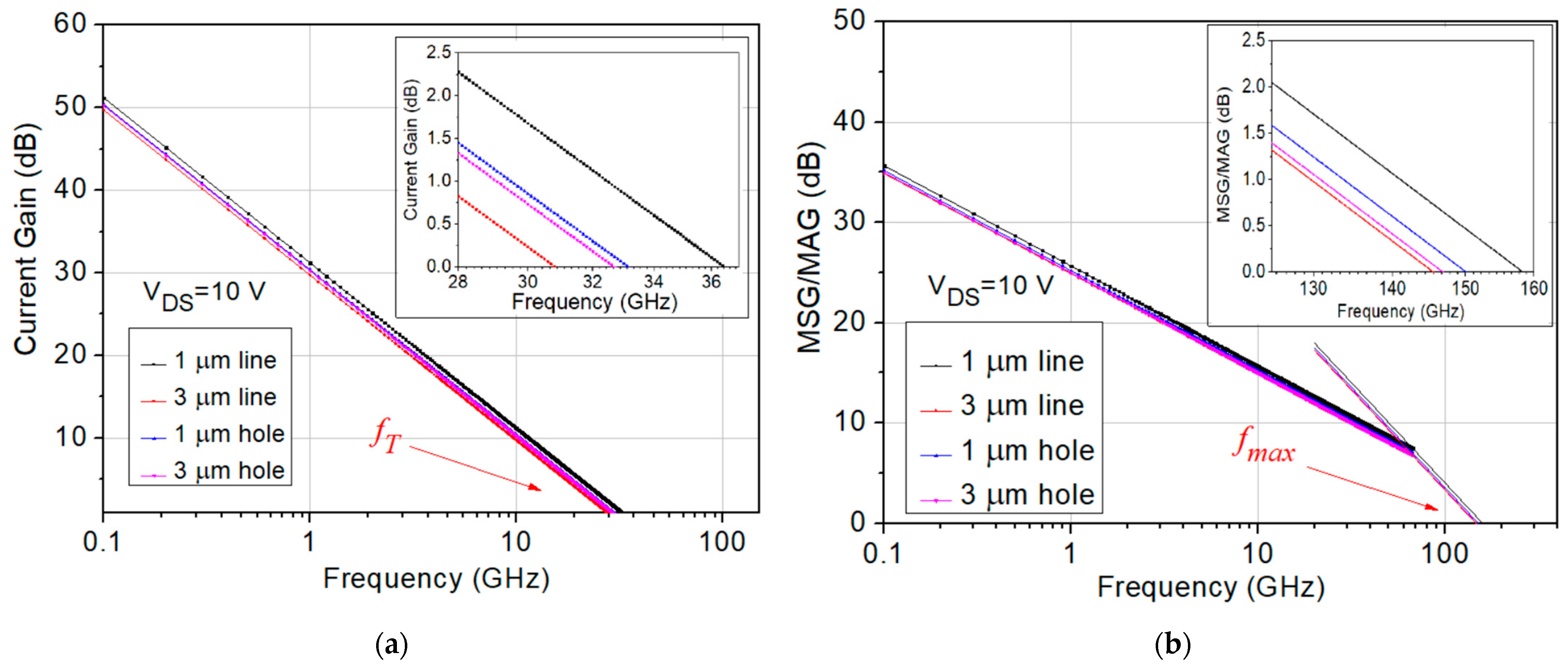
3.2.1. Small Signal Performance

All the designed AlGaN/GaN OEP devices were measured with a E8361C PNA network analyzer and a 4142B DC supplier to obtain the S parameter results for small signal performance analysis. The small-signal equivalent circuit model for the OEP AlGaN/GaN HEMTs was used, as shown in Figure 6. The small signal impedance matching system was calibrated with a short-open-load-thru (SOLT) calibration with an accuracy of less than ±0.01 dB for both the S21 and S12 values and less than −45 dB for both the S11 and S22 values within the measured frequency range [33]. The measured S parameters were first de-embedded and the current gain (H21), maximum stable power gain (MSG), and maximum available gain (MAG) were calculated using the Microwave Office 2000 software. After extrapolating the H21 (dB) to frequency (log scale) curves and MSG/MAG to frequency (log scale) curves with the slope of −20 dB/decade, the cut-off frequency (fT) and maximum oscillation frequency (fmax) values of the OEP devices were obtained, as shown in Figure 7a,b.
The de-embedded fT values of the designed 1 μm line, 3 μm line, 1 μm hole, and 3 μm hole OEP HEMTs are 36.40 GHz, 30.90 GHz, 33.10 GHz, and 32.60 GHz, respectively, as shown in Table 3. The de-embedded fmax values of the designed 1 μm line, 3 μm line, 1 μm hole, and 3 μm hole OEP HEMTs are 158.29 GHz, 145.50 GHz, 150.05 GHz, and 146.80 GHz, respectively, as shown in Table 3. Among the four designed OEP HEMTs with the gate width of 2 × 25 μm, the fT and fmax value of the 1 μm line OEP device exhibit the largest value of 36.4 GHz and 158.29 GHz, respectively.
The parasitic source resistance (Rs), parasitic drain resistance (Rd), parasitic gate-to-source capacitance (Cgs), and parasitic gate-to-drain capacitance (Cgd) of the four designed OEP HEMTs were also extracted from the S parameter results, as shown in Table 3. The 1 μm line OEP device exhibit the lowest Rs, Rd, Cgs, and Cgd of 4.35 Ω, 2.73 Ω, 91.03 fF, and 9.76 fF, respectively, among the four designed OEP HEMTs. The small signal results show that the 1 μm line OEP HEMTs exhibit the best small signal performance among the four designed structures, followed by the OEP HEMTs with the 1 μm holes, the 3 μm holes, and the 3 μm lines, in descending sequence.
The measured small signal characteristics of the four OEP HEMTs are shown in Figure 7 and Table 3. The results show that the 1 μm line OEP HEMT exhibited the highest fT and fmax among other OEP HEMTs, which could be attrbuted to the reduction in parasitic resistances and parasitic capacitances. The equations showing the correlation between fT, fmax, and the extracted parameters of Rs, Rd, Cgs, and Cgd are shown below in Equations (1) and (2) [34].
f T = g m 2 π C g s + C g d 1 + R s + R d g o + g m C g d R s + R d
f m a x = f T 2 g o R g + R i + R s + 2 π f T R g C g d
Equations (1) and (2) show that the fT and fmax value are inversely proportional to the parasitic components of Rs, Rd, Cgs, and Cgd.
The Rs, Rd, Cgs, and Cgd values of the four designed OEP HEMTs were analyzed and a similar ascending trend was found. The lowest parasitic values among the four designed structures were extracted from the 1 μm line OEP HEMTs, followed by the OEP HEMTs with the 1 μm holes, the 3 μm holes, and the 3 μm lines, in ascending sequence. This correlates to the trend of the fT and fmax value measured from the four designed OEP HEMTs. The extracted Cgs and Cgd values of both the 3 μm hole and 3 μm line OEP HEMT are larger than the extracted Cgs and Cgd values of both the 1 μm hole and 1 μm line OEP HEMT, which shows that the increment in the size of the patterns from 1 μm to 3 μm increases the Cgs and Cgd values. The extracted Cgs and Cgd values of the hole OEP HEMTs also show larger values than the line OEP HEMTs, which is due to the increased separated ohmic metal arrays formed by the hole patterns. The increase in the contact area between the ohmic metal and the AlGaN barrier layer were used to reduce the contact resistance of the OEP HEMTs, and the results show that the 1 μm line OEP HEMT could be fabricated with the best improvement in small signal performance at the Ka band.

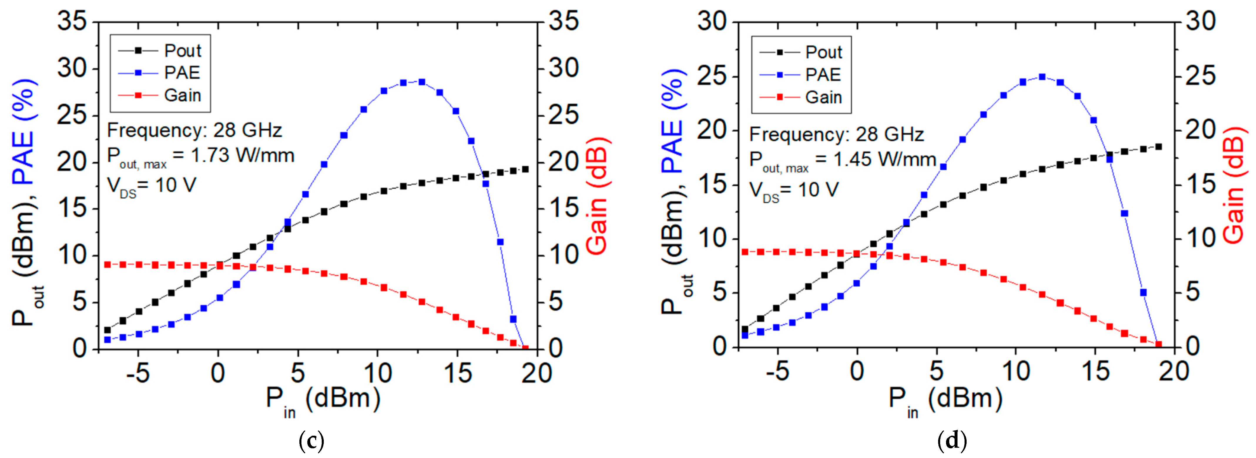
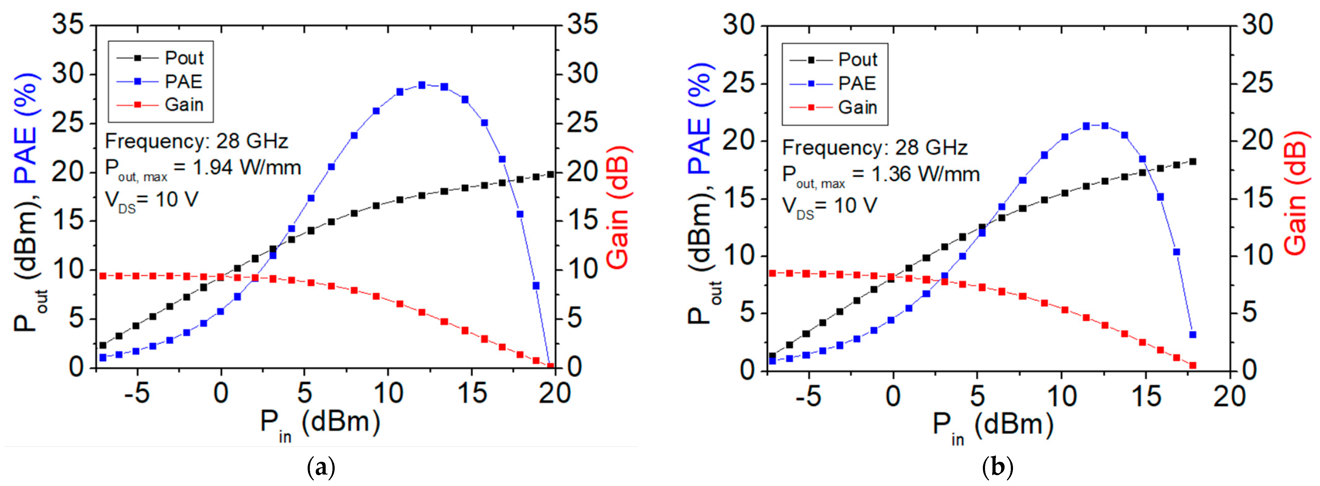
3.2.2. Large Signal Performance
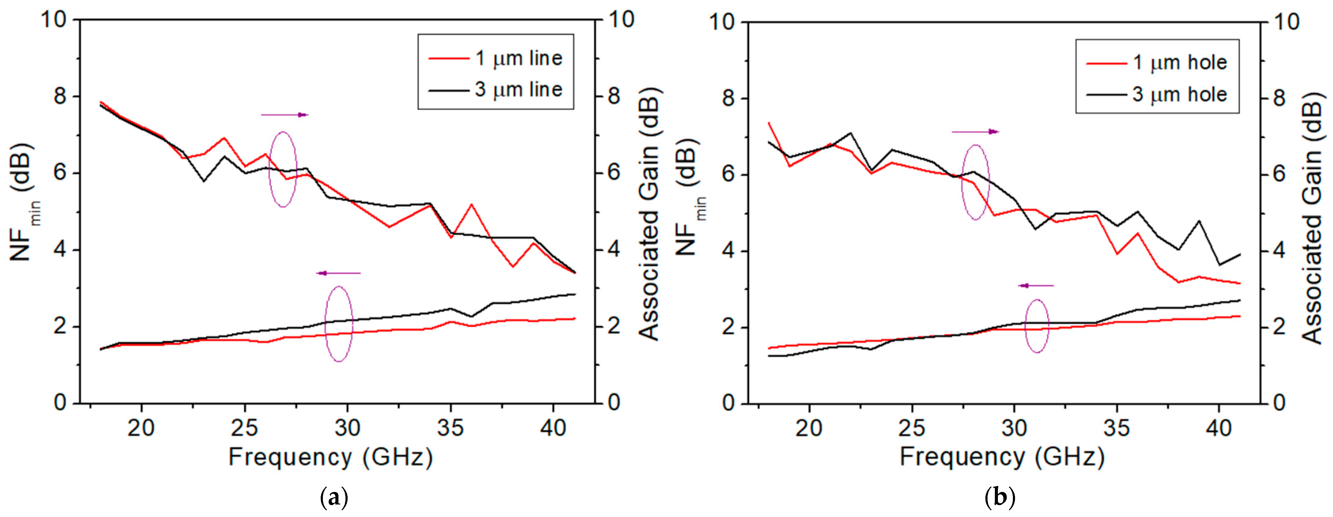
Load–pull measurements at 28 GHz operation frequency for RF power and PAE analysis were also conducted for the four designed OEP devices with a gate width of 2 × 25 μm. The power sweep curves of the load–pull measurement with input power set from −7.5 dBm to 20 dBm for the four designed OEP device structures with 1 μm lines, 3 μm lines, 1 μm holes, and 3 μm holes are shown in Figure 8a,b,c,d, respectively.
The peak PAE, the power gain, and the maximum output power density (Pout, max) in units of dBm and W/mm of the four OEP HEMTs are shown in Table 4. The peak PAE of the 1 μm line, 3 μm line, 1 μm hole, and 3 μm hole HEMTs are 29.01%, 21.44%, 28.70%, and 25.03%, respectively. The power gain of the 1 μm line, 3 μm line, 1 μm hole, and 3 μm hole HEMTs are 9.52 dB, 8.60 dB, 9.12 dB, and 8.87 dB, respectively. The Pout, max (dBm) of the 1 μm line, 3 μm line, 1 μm hole, and 3 μm hole HEMTs are 19.86 dBm, 18.31 dBm, 19.36 dBm, and 18.60 dBm, respectively. The Pout, max (W/mm) of the 1 μm line, 3 μm line, 1 μm hole, and 3 μm hole HEMTs are 1.94 W/mm, 1.36 W/mm, 1.73 W/mm, and 1.45 W/mm, respectively. The load–pull results show that the 1 μm line OEP HEMTs exhibit the best large signal performance among the four designed structures, followed by the OEP HEMTs with the 1 μm holes, the 3 μm holes, and the 3 μm lines, in descending sequence.
The measured large signal characteristics of the four OEP HEMTs are shown in Figure 8 and Table 4. The 1 μm line OEP HEMTs exhibit the largest gain, PAE, and Pout, max among the four designed OEP HEMTs, followed by the OEP HEMTs with the 1 μm holes, the 3 μm holes, and the 3 μm lines, in descending sequence. The descending trend obtained from the large signal performance shown in Table 4 matches that of the DC characteristics and the small signal performances shown in Table 2 and Table 3, respectively. This could be due to the good thermal dissipation from the SiC substrate and low surface trapping of the OEP HEMTs with well deposited passivation layer [35]. The increase in the contact area between the ohmic metal and the AlGaN barrier layer was used to reduce the contact resistance and increase the saturation current of the OEP HEMTs, and the results show that the 1 μm line OEP HEMT could be fabricated with the best improvement in large signal performance at the Ka band.

3.2.3. Noise Figure

The noise figure measurement at the Ka band was carried out for all four OEP devices with a gate width of 2 × 25 μm. The frequency sweep for the noise figure measurement was set from 18 GHz to 41 GHz. The gain to NFmin graphs of the line-etched and hole-etched devices are shown in Figure 9a,b, respectively. At 28 GHz, NFmin of 1.75 dB with an associated gain of 5.98 dB and NFmin of 2.00 dB with an associated gain of 6.14 dB were measured for the 1 μm line and 3 μm line OEP devices, respectively, as shown in Figure 9a and Table 2. At 28 GHz, NFmin of 1.85 dB with an associated gain of 5.80 dB and NFmin of 1.87 dB with an associated gain of 6.09 dB were measured for the 1 μm hole and 3 μm hole OEP devices, respectively, as shown in Figure 9b and Table 2. The results show that the OEP devices etched with 1 μm lines exhibit the lowest NFmin among the fabricated devices with comparable associated gain.
The measured noise figure characteristics of the four OEP HEMTs are shown in Figure 9 and Table 2. The 1 μm line OEP HEMTs exhibit the smallest NFmin among the four designed OEP HEMTs at 28 GHz, followed by the OEP HEMTs with the 1 μm holes, the 3 μm holes, and the 3 μm lines, in ascending sequence. The lowered NFmin is due to the reduction of access resistance achieved from the thinned barrier layer at the ohmic patterns and the increased contact area at the ohmic metal and semiconductor interface, which reduce Rs and Rd [19]. However, larger areas of the etched-away barrier layers in the 3 μm line OEP devices cause larger depletion of the 2DEG and reduction in IDS, which further increase Rs and Rd [20]. The increased Rs and Rd in the 3 μm line OEP devices may also be the reason for the higher NFmin, as shown in Equation (3). On the other hand, the parasitic Cgs of the HEMT devices also plays an important role in determining the device NFmin during high frequency noise figure measurement, as shown in Equation (3) [36]. The parasitic Cgs values of the four designed OEP HEMTs are extracted, as shown in Table 3, and show a similar ascending trend to that of the ascending trend found in the measured NFmin values of the four designed OEP HEMTs, as shown in Table 2.
N F m i n = 1 + 2 π f K f C g s R g + R s g m
The increase in the contact area between the ohmic metal and the AlGaN barrier layer was used to reduce the Rs and Rd of the OEP HEMTs, and the results show that the 1 μm line OEP HEMT could be fabricated with the best improvement in noise figure performance at the Ka band.
Further analysis comparing the device performance of GaN HEMTs with and without the 1 μm OEP structure could be pursued as future work. This analysis might involve exploring various ohmic etching depths to optimize contact resistivity.

4. Conclusions

The design and fabrication of AlGaN/GaN HEMTs with four different OEPs to optimize the Ka-band performances were discussed in this study. The 1 μm line, 3 μm line, 1 μm hole, and 3 μm hole OEP AlGaN/GaN HEMTs were analyzed with regard to DC and RF characteristics. Low ρc of 4.04 × 10⁻⁷ Ω·cm2 was also measured for the 1 μm line OEP HEMTs. Optimized Gm of 403 mS/mm and the IDSS of 999 mA/mm were measured for the 1 μm line OEP HEMT. The small signal and large signal results of the OEP HEMTs were measured and the optimized performance achieved with the 1 μm line OEP HEMT. Moreover, the lowest NFmin of 1.75 dB among four OEP HEMTs was achieved with the fabricated 1 μm line OEP HEMTs, showing improvement in the RF noise figure characteristics. Overall, the increase in the contact area between the ohmic metal and the AlGaN barrier layer were used to reduce the contact resistance of the OEP HEMTs, and the results show that the 1 μm line OEP HEMT could be fabricated with the best improvement in RF performance for future 5G and B5G system applications at the Ka-band.

Author Contributions

Conceptualization, M.-W.L., C.-W.C. and Y.-C.L.; methodology, M.-W.L., C.-W.C. and Y.-C.L.; validation, Y.-C.L. and E.-Y.C.; formal analysis, M.-W.L., C.-W.C. and Y.-C.L.; investigation, M.-W.L., C.-W.C. and Y.-C.L.; resources, Y.-C.L. and E.-Y.C.; data curation, M.-W.L., C.-W.C. and Y.-C.L.; writing—original draft preparation, M.-W.L. and Y.-C.L.; writing—review and editing, F.G., Y.-C.L. and E.-Y.C.; visualization, M.-W.L., C.-W.C., Y.-C.L. and F.G.; supervision, F.G. and E.-Y.C.; project administration, Y.-C.L. and E.-Y.C.; funding acquisition, F.G., Y.-C.L. and E.-Y.C. All authors have read and agreed to the published version of the manuscript.

Funding

This research was financially supported in part by the National Science and Technology Council, Taiwan (project number: NSTC 111-2218-E-A49-018, NSTC 111-2634-F-A49-008, NSTC 111-2221-E-A49-173-MY3, and NSTC 112-2622-8-A49-013–SB), by the Co-creation Platform of the Industry-Academia Innovation School, NYCU, under the framework of the National Key Fields Industry-University Cooperation and Skilled Personnel Training Act, from the Ministry of Education (MOE), the National Development Fund (NDF), and industry partners in Taiwan.

Data Availability Statement

Data are contained within the article.

Acknowledgments

We acknowledge the Taiwan Semiconductor Research Institute (TSRI), Taiwan, for providing RF measurement support, the Centre for Research in Information and Communication Technologies of the University of Granada (CITIC-UGR), Spain, for funding support and the Compound Semiconductor Device Laboratory, NYCU, Taiwan, for wafer fabrication and DC measurement support.

Conflicts of Interest

The authors declare no conflicts of interest. The funders had no role in the design of the study; in the collection, analyses, or interpretation of data; in the writing of the manuscript; or in the decision to publish the results.

References

  1. Zanella, A.; Bui, N.; Castellani, A.; Vangelista, L.; Zorzi, M. Internet of Things for Smart Cities. IEEE Internet Things J. 2014, 1, 22–32. [Google Scholar] [CrossRef]
  2. McEnroe, P.; Wang, S.; Liyanage, M. A Survey on the Convergence of Edge Computing and AI for UAVs: Opportunities and Challenges. IEEE Internet Things J. 2022, 9, 15435–15459. [Google Scholar] [CrossRef]
  3. Al-Ali, A.R.; Zualkernan, I.A.; Rashid, M.; Gupta, R.; Alikarar, M. A smart home energy management system using IoT and big data analytics approach. IEEE Trans. Consum. Electron. 2017, 63, 426–434. [Google Scholar] [CrossRef]
  4. Lorincz, J.; Klarin, Z.; Ožegović, J. A Comprehensive Overview of TCP Congestion Control in 5G Networks: Research Challenges and Future Perspectives. Sensors 2021, 21, 4510. [Google Scholar] [CrossRef] [PubMed]
  5. Liu, W.; Michelson, D.G. Effect of Turbulence Layer Height and Satellite Altitude on Tropospheric Scintillation on Ka-Band Earth–LEO Satellite Links. IEEE Trans. Veh. Technol. 2010, 59, 3181–3192. [Google Scholar] [CrossRef]
  6. Nakatani, K.; Komatsuzaki, Y.; Shinjo, S.; Kamioka, J.; Komaru, R.; Nakamizo, H.; Miyawaki, K.; Yamanaka, K. A highly integrated RF frontend module including Doherty PA, LNA and switch for high SHF wide-band massive MIMO in 5G. In Proceedings of the 2017 IEEE Topical Conference on RF/Microwave Power Amplifiers for Radio and Wireless Applications (PAWR), Phoenix, AZ, USA, 15–18 January 2017; pp. 37–39. [Google Scholar] [CrossRef]
  7. Ellinger, F.; Claus, M.; Schröter, M.; Carta, C. Review of advanced and Beyond CMOS FET technologies for radio frequency circuit design. In Proceedings of the 2011 SBMO/IEEE MTT-S International Microwave and Optoelectronics Conference (IMOC 2011), Natal, Brazil, 29 October–1 November 2011; pp. 347–351. [Google Scholar] [CrossRef]
  8. Mehr, P.; Moallemi, S.; Zhang, X.; Lepkowski, W.; Kitchen, J.; Thornton, T.J. CMOS-Compatible MESFETs for High Power RF Integrated Circuits. IEEE Trans. Semicond. Manuf. 2019, 32, 14–22. [Google Scholar] [CrossRef]
  9. Lin, Y.-C.; Chang, E.Y.; Yamaguchi, H.; Wu, W.-C.; Chang, C.-Y. A δ-Doped InGaP/InGaAs pHEMT with Different Doping Profiles for Device-Linearity Improvement. IEEE Trans. Electron Devices 2007, 54, 1617–1625. [Google Scholar] [CrossRef]
  10. del Alamo, J.A. The High Electron Mobility Transistor. In 75th Anniversary of the Transistor; IEEE: Piscataway, NJ, USA, 2023; pp. 253–262. [Google Scholar] [CrossRef]
  11. Mishra, U.K.; Parikh, P.; Wu, Y.-F. AlGaN/GaN HEMTs-an overview of device operation and applications. Proc. IEEE 2022, 90, 1022–1031. [Google Scholar] [CrossRef]
  12. Lee, M.-W.; Lin, Y.-C.; Chang, P.-S.; Tsao, Y.-F.; Hsu, H.-T.; Dee, C.-F.; Chang, E.Y. Over 10 W/mm High Power Density AlGaN/GaN HEMTs with Small Gate Length by the Stepper Lithography for Ka-Band Applications. IEEE J. Electron Devices Soc. 2023, 11, 311–318. [Google Scholar] [CrossRef]
  13. Palacios, T.; Chakraborty, A.; Rajan, S.; Poblenz, C.; Keller, S.; DenBaars, S.; Speck, J.; Mishra, U. High-power AlGaN/GaN HEMTs for Ka-band applications. IEEE Electron Device Lett. 2005, 26, 781–783. [Google Scholar] [CrossRef]
  14. Nakatani, K.; Yamaguchi, Y.; Komatsuzaki, Y.; Sakata, S.; Shinjo, S.; Yamanaka, K. A Ka-Band High Efficiency Doherty Power Amplifier MMIC using GaN-HEMT for 5G Application. In Proceedings of the 2018 IEEE MTT-S International Microwave Workshop Series on 5G Hardware and System Technologies (IMWS-5G), Dublin, Ireland, 30–31 August 2018; pp. 1–3. [Google Scholar] [CrossRef]
  15. Xu, H.; Sanabria, C.; Chini, A.; Keller, S.; Mishra, U.K.; York, R.A. A C-band high-dynamic range GaN HEMT low-noise amplifier. IEEE Microw. Wirel. Compon. Lett. 2004, 14, 262–264. [Google Scholar] [CrossRef]
  16. Palacios, T.; Chakraborty, A.; Heikman, S.; Keller, S.; DenBaars, S.P.; Mishra, U.K. AlGaN/GaN high electron mobility transistors with InGaN back-barriers. IEEE Electron Device Lett. 2006, 27, 13–15. [Google Scholar] [CrossRef]
  17. Gibiino, G.P.; Angelotti, A.M.; Santarelli, A.; Florian, C. Microwave Characterization of Trapping Effects in 100-nm GaN-on-Si HEMT Technology. IEEE Microw. Wirel. Compon. Lett. 2019, 29, 604–606. [Google Scholar] [CrossRef]
  18. Guo, J.; Li, G.; Faria, F.; Cao, Y.; Wang, R.; Verma, J.; Gao, X.; Guo, S.; Beam, E.; Ketterson, A.; et al. MBE-Regrown Ohmics in InAlN HEMTs With a Regrowth Interface Resistance of 0.05 Ω·mm. IEEE Electron Device Lett. 2012, 33, 525–527. [Google Scholar] [CrossRef]
  19. Takei, Y.; Kamiya, M.; Tsutsui, K.; Saito, W.; Kakushima, K.; Wakabayashi, H.; Kataoka, Y.; Iwai, H. Ohmic Contact Properties Depending on AlGaN Layer Thickness for AlGaN/GaN High Electron Mobility Transistor Structures. ECS Trans. 2014, 61, 265–270. [Google Scholar] [CrossRef]
  20. Lu, Y.; Ma, X.; Yang, L.; Hou, B.; Mi, M.; Zhang, M.; Zheng, J.; Zhang, H.; Hao, Y. High RF Performance AlGaN/GaN HEMT Fabricated by Recess-Arrayed Ohmic Contact Technology. IEEE Electron Device Lett. 2018, 39, 811–814. [Google Scholar] [CrossRef]
  21. Benakaprasad, B.; Eblabla, A.M.; Li, X.; Crawford, K.G.; Elgaid, K. Optimization of Ohmic Contact for AlGaN/GaN HEMT on Low-Resistivity Silicon. IEEE Trans. Electron Devices 2020, 67, 863–868. [Google Scholar] [CrossRef]
  22. Wang, C.; Zhao, M.D.; He, Y.L.; Zheng, X.F.; Wei, X.X.; Mao, W.; Zhang, J.; Hao, Y. Optimization of ohmic contact for AlGaN/GaN HEMT by introducing patterned etching in ohmic area. Solid State Electron. 2017, 129, 114–119. [Google Scholar] [CrossRef]
  23. You, X.-R.; Chen, C.-W.; Tzou, J.; Hsin, Y.-M. Study of Au-based and Au-free Ohmic contacts in AlGaN/GaN HEMTs by recessed patterns. ECS J. Solid State Sci. Technol. 2021, 10, 075006. [Google Scholar] [CrossRef]
  24. Takei, Y.; Kamiya, M.; Tsutsui, K.; Saito, W.; Kakushima, K.; Wakabayashi, H.; Kataoka, Y.; Iwai, H. Reduction of contact resistance on AlGaN/GaN HEMT structures introducing uneven AlGaN layers. Phys. Status Solidi A 2015, 212, 1104–1109. [Google Scholar] [CrossRef]
  25. Wang, C.; He, Y.; Zheng, X.; Zhao, M.; Mi, M.; Li, X.; Mao, W.; Ma, X.; Hao, Y. Low ohmic-contact resistance in AlGaN/GaN high electron mobility transistors with holes etching in ohmic region. Electron. Lett. 2015, 51, 2145–2147. [Google Scholar] [CrossRef]
  26. Han, K. Employing hole-array recess of barrier layer of AlGaN/GaN heterostructures to reduce annealing temperature of ohmic contact. Semicond. Sci. Technol. 2017, 32, 105010. [Google Scholar] [CrossRef]
  27. Jang, M.; Park, J.; Hwang, J.H.; Mun, H.J.; Cha, S.; Hong, S.-M.; Jang, J.-H. Effects of periodic patterns in recessed ohmic contacts on InAlGaN/GaN heterostructures. Solid-State Electron. 2020, 174, 107917. [Google Scholar] [CrossRef]
  28. Hajlasz, M.; Donkers, J.J.T.M.; Sque, S.J.; Heil, S.B.S.; Gravesteijn, D.J.; Rietveld, F.J.R.; Schmitz, J. Characterization of recessed Ohmic contacts to AlGaN/GaN. In Proceedings of the 2015 International Conference on Microelectronic Test Structures, Tempe, AZ, USA, 23–26 March 2015; pp. 158–162. [Google Scholar] [CrossRef]
  29. Buttari, D.; Heikman, S.; Keller, S.; Mishra, U.K. Digital etching for highly reproducible low damage gate recessing on AlGaN/GaN HEMTs. In Proceedings of the IEEE Lester Eastman Conference on High Performance Devices, Newark, DE, USA, 8 August 2002; pp. 461–469. [Google Scholar] [CrossRef]
  30. Romanczyk, B.; Zheng, X.; Guidry, M.; Li, H.; Hatui, N.; Wurm, C.; Krishna, A.; Ahmadi, E.; Keller, S.; Mishra, U.K. W-Band Power Performance of SiN-Passivated N-Polar GaN Deep Recess HEMTs. IEEE Electron Device Lett. 2020, 41, 349–352. [Google Scholar] [CrossRef]
  31. Kim, D.-H.; del Alamo, J.A. 30-nm InAs Pseudomorphic HEMTs on an InP Substrate with a Current-Gain Cutoff Frequency of 628 GHz. IEEE Electron Device Lett. 2008, 29, 830–833. [Google Scholar] [CrossRef]
  32. Buttari, D.; Chini, A.; Meneghesso, G.; Zanoni, E.; Moran, B.; Heikman, S.; Zhang, N.; Shen, L.; Coffie, R.; DenBaars, S.; et al. Systematic characterization of Cl2 reactive ion etching for improved ohmics in AlGaN/GaN HEMTs. IEEE Electron Device Lett. 2002, 23, 76–78. [Google Scholar] [CrossRef]
  33. Kumazaki, Y.; Ozaki, S.; Okamoto, N.; Hara, N.; Ohki, T. Low-Resistance and Low-Thermal-Budget Ohmic Contact by Introducing Periodic Microstructures for AlGaN/AlN/GaN HEMTs. IEEE Trans. Electron Devices 2022, 69, 3073–3078. [Google Scholar] [CrossRef]
  34. Lee, P.-H.; Lin, Y.-C.; Hsu, H.-T.; Tsao, Y.-F.; Dee, C.-F.; Su, P.; Chang, E.Y. A Tall Gate Stem GaN HEMT With Improved Power Density and Efficiency at Ka-Band. IEEE J. Electron Devices Soc. 2023, 11, 36–42. [Google Scholar] [CrossRef]
  35. Binari, S.; Ikossi, K.; Roussos, J.A.; Kruppa, W.; Park, D.; Dietrich, H.B.; Koleske, D.D.; Wickenden, A.E.; Henry, R.L. Trapping effects and microwave power performance in AlGaN/GaN HEMTs. IEEE Trans. Electron Devices 2001, 48, 465–471. [Google Scholar] [CrossRef]
  36. Jarndal, A.; Arivazhagan, L.; Almajali, E.; Majzoub, S.; Bonny, T.; Mahmoud, S. Impact of AlGaN Barrier Thickness and Substrate Material on the Noise Characteristics of GaN HEMT. IEEE J. Electron Devices Soc. 2022, 10, 696–705. [Google Scholar] [CrossRef]
Figure 1. Schematic graph of the OEP AlGaN/GaN HEMT with the (a) cross-section view and the (b) top view.
Micromachines 15 00081 g001
Figure 2. Optical microscope pictures of the developed OEPs with (a) 1 μm lines, (b) 3 μm lines, (c) 1 μm holes, and (d) 3 μm holes.
Micromachines 15 00081 g002
Figure 3. IDS−VGS and Gm−VGS curves for the 2 × 25 μm AlGaN/GaN HEMTs with different OEPs. (Left arrow: IDS; Right arrow: Gm).
Micromachines 15 00081 g003
Figure 4. Ron and IDS–VDS curves for the four 2 × 25 μm AlGaN/GaN OEP HEMTs.
Micromachines 15 00081 g004
Figure 5. Benchmark of the lowest contact resistance in this study with published literature [20,21,22,23,25,26,27].
Micromachines 15 00081 g005
Figure 6. Small-signal equivalent circuit model for the AlGaN/GaN HEMTs with the hole OEPs.
Micromachines 15 00081 g006
Figure 7. (a) Current gain to frequency plot and (b) MSG/MAG to frequency plot for the 2 × 25 μm OEP AlGaN/GaN HEMTs.
Micromachines 15 00081 g007
Figure 8. Load–pull curves at 28 GHz operation frequency for the 2 × 25 μm OEP AlGaN/GaN HEMTs with (a) 1 μm lines, (b) 3 μm lines, (c) 1 μm holes, and (d) 3 μm holes.
Micromachines 15 00081 g008aMicromachines 15 00081 g008b
Figure 9. NFmin- Frequency curves for the 2 × 25 μm OEP AlGaN/GaN HEMTs with (a) etched-line patterns and (b) etched-hole patterns. (Left arrow: NFmin; right arrow: gain).
Micromachines 15 00081 g009
Table 1. Contact resistivity and contact resistance results of different OEP structures obtained with the TLM method.
Ohmic Etching Patternsρc (Ω·cm2)Rc (Ω·mm)
1 μm line4.04 × 10−70.154
3 μm line7.80 × 10−70.212
1 μm hole6.01 × 10−70.191
3 μm hole7.68 × 10−70.199
w/o OEPs 2.73 × 10−60.429
Table 2. Ron, Gm, peak, IDSS, minimum noise figure at 28 GHz, and associated gain at 28 GHz of the 2 × 25 μm AlGaN/GaN HEMT devices with different OEP structures.
Ohmic Etching PatternsRon
(Ω·mm)
Gm, peak
(mS/mm)
IDSS
(mA/mm)
NFmin at 28 GHz (dB)Gain at 28 GHz
(dB)
1 μm line1.614039991.755.98
3 μm line2.243748552.006.14
1 μm hole1.633939321.855.80
3 μm hole1.813858801.876.09
Table 3. fT, fmax, and extracted small signal parameters of the 2 × 25 μm AlGaN/GaN HEMT devices with different OEP structures.
Ohmic Etching PatternsfT
(GHz)
fmax
(GHz)
Rs
(Ω)
Rd
(Ω)
Cgs
(fF)
Cgd
(fF)
1 μm line36.40158.294.352.7391.039.76
3 μm line30.90145.505.043.4394.8410.82
1 μm hole33.10150.054.532.8191.3010.15
3 μm hole32.60146.804.752.9393.4210.56
Table 4. RF large signal load-pull measurement results of the 2 × 25 μm AlGaN/GaN HEMT devices with different OEP structures.
Ohmic Etching
Patterns
PAE Peak
(%)
Gain
(dB)
Pout, max
(dBm)
Pout, max
(W/mm)
1 μm line29.019.5219.861.94
3 μm line21.448.6018.311.36
1 μm hole28.709.1219.361.73
3 μm hole25.038.8718.601.45
Disclaimer/Publisher’s Note: The statements, opinions and data contained in all publications are solely those of the individual author(s) and contributor(s) and not of MDPI and/or the editor(s). MDPI and/or the editor(s) disclaim responsibility for any injury to people or property resulting from any ideas, methods, instructions or products referred to in the content.

