You are currently viewing a new version of our website. To view the old version click .
Sustainability
  • Article
  • Open Access

6 February 2025

Indium Phosphide Semiconductor Technology for Next-Generation Communication Systems: Sustainability and Material Considerations

,
,
,
,
,
,
and
1
CEA-Leti, Université Grenoble Alpes, F-38000 Grenoble, France
2
InPACT, Pombliere, F-73600 Saint Marcel, France
*
Author to whom correspondence should be addressed.
This article belongs to the Special Issue Advanced Materials and Technologies for Environmental Sustainability

Abstract

Indium phosphide (InP) semiconductor technology is being explored for radiofrequency (RF) applications, targeting frequencies exceeding 100 GHz, to support the next generation of 6G communication systems. When taking into account sustainability in designing this future generation, growing concerns are emerging regarding the environmental impact of communication networks and the reliance on raw materials for the production of Information and Communication Technologies (ICTs). The extraction, processing, and manufacturing of such materials and semiconductor technologies result in environmental impacts, but these impacts remain insufficiently documented. Firstly, this study evaluates the environmental impacts of manufacturing indium phosphide (InP) wafers based on industrial data and those of InP-based heterojunction bipolar transistors (HBTs) based on early-stage research data. Secondly, this study attempts to highlight the challenges posed by the increasing demand for high-tech solutions, involving raw materials, by evaluating the potential demand for indium for RF 6G applications, with a deployment scenario.

1. Introduction

The Information and Communications Technology (ICT) sector represented between 2.1 and 3.9% of global greenhouse gas (GHG) emissions in 2020 [1]. Life cycle assessment (LCA) shows that ICT’s world carbon footprint mainly comes from the use phase of user devices (44%) and the manufacturing of user devices (28%) [2]. A high share of the environmental impacts during user device manufacturing (smartphones and tablets) comes from the production of silicon semiconductor-based integrated circuits (ICs) [3,4,5]. IC manufacturing includes substrate production and wafer processing.
The development of III–V compound-based technologies, such as indium phosphide (InP) heterojunction bipolar transistors (HBTs), is currently investigated in order to ensure the amplification and reception functions of sub-THz electromagnetic waves with increased energy efficiency for the next generation of communication systems (6G) [6]. For instance, for Power Amplifier (PA) operation, InP HBTs enable breakdown voltage 4 times higher than InP high-electron-mobility transistors (HEMTs) and silicon–germanium (SiGe) HBTs with frequency expected above 100 GHz. They are fabricated currently at high cost on small InP wafers. Research is ongoing towards new ways to build InP transistors on silicon (Si) wafers in order to allow their production at a large scale. The most advanced are Smart CutTM technology, which is based on wafer bonding, layer transfer techniques, and tiling [7], and Nano-Ridge Engineering (NRE), which is based on the epitaxy of III–V layers on silicon [8]. The CEA-Leti roadmap on this topic consists in facilitating the 3D integration of InP-BHTs with CMOS using SmartCutTM technology [9,10].
However, while the environmental impacts of silicon substrates have already been investigated [11,12], few studies have been carried out on InP substrates [13], making it difficult to have a reliable environmental assessment of the fabrication of InP technologies [8]. Indium is currently used for ICT applications such as flat panel displays, solders, semiconductors, and LEDs (25 t/year in 2020 in France). The increase in electronic devices may lead to an increase in this indium consumption, up to 5 times in 2050 for the high-demand scenario with high IoT deployment [14]. Therefore, beyond the environmental impact of fabrication, the demand for indium linked to the development of new technologies must also be scrutinized.
The main contributions of this study are as follows:
(1)
Production of knowledge and data on the environmental impacts of commercially available InP wafers in order to provide more accurate results;
(2)
Evaluation of the environmental impacts at an early stage of R&D of the InP heterojunction bipolar transistor fabrication process on Si in order to help make better technological choices;
(3)
Estimation of indium material requirements with the deployment of this technology for 6G application.

2. Environmental Impacts of Manufacturing Indium Phosphide (InP) Wafers and InP-Based Heterojunction Bipolar (HBT) Transistors

2.1. Methods

The study follows the International Organization for Standardization’s (ISO) 14040:44 standard [15] and the Product Environmental Footprint (PEF) methodology developed by the European Commission [16]. Environmental impacts are evaluated with the Environmental Footprint method (EF3.1) using the ecoinvent 3.9.1 database and Simapro software (version 9.6). The production takes place in France, with a nuclear base electricity mix (electricity low voltage in France: 0.09 kg CO2/kWh; 71% of nuclear in ecoinvent 3.9.1), as InP wafer producer InPACT and semiconductor manufacturers have production sites in France.

2.2. InP Wafers

System Description

The goals of this Life Cycle Assessment are to quantify the environmental impacts of the cradle-to-gate production of InP wafers and identify the main contributors along the fabrication chain. The functional unit is “production of 1 m2 of InP single-crystal wafer with 512 µm thickness”.
The InP wafer fabrication starts with the extraction of raw materials: indium and phosphide (Figure 1). Electricity consumption for indium purification up to 6N based on Smith was added in the inventory [17]. The first step is the preparation of the InP polycrystal [18], which is usually obtained with the gradient freeze growth method, derived from the horizontal Bridgman technique: a crucible containing indium occupies an extremity of a quartz bulb, and the other extremity is filled with phosphorus. The quartz bulb is placed in an oven, itself placed in an autoclave. The indium zone is heated above 1062 °C (which is the fusion temperature of indium) and the phosphorus zone is maintained at around 560 °C (where phosphorus is volatile). Phosphorus reacts with indium to form liquid InP. The InP polycrystal is obtained by cooling.
Figure 1. InP wafer fabrication.
Then, the monocrystal material is obtained by the melting and controlled recrystallization of the polycrystal [18] (Figure 1). There are two techniques: vapor pressure-controlled Czochralski (pCZ) and vertical Bridgman. pCZ is a pulling growth method. The InP monocrystal is pulled up from the InP melt in the crucible within a tight inner chamber. The chamber has an independently heated reservoir of condensed phase phosphorus to maintain a controlled phosphorus pressure. Optimized graphite heaters are placed around the chamber. Bridgman is a boat growth method. The InP monocrystal is grown by solidifying the InP melt from a seed crystal placed in a bottom-seeded crucible. A set of graphite resistance heaters are regulated separately to guarantee the solidification by sliding the thermal profile along the crucible. In both cases, the growth assembly and the heater system are enclosed in a water-cooled, high-pressure, stainless steel vessel. Boron oxide (B2O3) acts as an encapsulant, suppressing phosphorus evaporation. The power is controllably ramped down until the entire charge is solidified with the surrounding insulation designed to produce a smooth thermal profile. The InP single crystal can be doped at this stage by introducing impurities such as iron, tin, or zinc in the bath. For this life cycle assessment of InP, we have considered the vapor pressure-controlled Czochralski fabrication (pCZ); for further investigations, we could work on the Bridgman fabrication. Both technologies are used and are complementary in the market depending on diameter, dopant, and applications.
The InP single crystal ingot is oriented to identify crystallographic orientation, then trimmed to the required diameter (cylindrical grinding). The orientation flats are machined to identify the crystal direction. The InP ingot is sliced into wafers with a diamond saw. The wafers’ surface and bevel are polished. Wafers are then cleaned, and the surface is prepared with chemicals such as phosphoric acid, sulfuric acid, hydrochloric acid, and hydrogen peroxide [19] to have the surface ready for epitaxy with a minimum of impurities, particles, and the right flatness. Finally, wafers are packaged in a way that maintains the surface cleanliness [20].
Seed and tail parts of ingots are not used to make wafers because of the Czochralski pulling shape and because they might contain more impurities than the rest of the ingot. These ingot extremities are considered as by-products, not planned as a product but having an economic value. Indeed, they are sold to be reused for other industrial uses that require InP of lower purity. Slicing and grinding waste are considered waste, as they are not recycled nor reused in another production (Figure 1).
The ISO 14044 guidelines [21] and PEF method [16] recommend system expansion and indicate that economic allocation should only be used as a last resort, when other methods are not suitable. Here, the ingot extremities and the wafers come from the same ingot, so the environmental impacts cannot be calculated separately with system expansion. Allocation of the environmental impacts between the InP wafers and the ingot extremities was defined according to economic allocation (80% for the wafers, 20% for the ingot extremities), considering that the wafers are the main product. A sensibility analysis is realized in Section 2.3.2. to evaluate the influence of this allocation parameter on the environmental impacts.

2.3. Life Cycle Inventory of InP Wafer

The data were collected in 2021 at the InPACT Moûtiers industrial site in France, based on a reference period of production. The factory produces InP wafers of different sizes: 2′′, 3′′, and 4′′. It was not possible to separate inputs and outputs depending on wafer sizes. However, the process of fabrication is similar between all wafer sizes. The impact assessment was carried out for the total mass of raw materials used in the industrial process for a reference period. The average wafer area is 3869 mm2/wafer and the average wafer thickness is 512 µm. All inputs and outputs to manufacture 1 m2 of InP wafer are collected and described in Table 1.
Table 1. Life cycle inventory for functional unit: 1 m2 of 512 µm thick InP single crystalline wafer.

2.3.1. Results of Life Cycle Impact Assessment of InP Wafer

Normalization and weighting methods recommended by the EU bring out the following relevant indicators to investigate: resource use, minerals and metals (kg Sb eq), resource use, fossils (MJ), human toxicity, non-cancer (CTUh), climate change (kg CO2eq), ecotoxicity, freshwater (CTUe) (which contributes to 84% of single score) [16]. Those indicators are selected for the contribution analysis.
Figure 2 shows the main contributors to the environmental impacts: indium 6N (6N meaning 99.9999% purity) production, electricity consumption, chemical production, and wastewater treatment.
Figure 2. Contribution analysis per environmental indicator, with French electricity mix.
Indium 6N production requires, indeed, lots of energy to refine the metals to a high purity level. Indium 6N production contributes 93% to mineral and metal resource use and is one of the main contributors to freshwater eutrophication, freshwater ecotoxicity, and human toxicity indicators. Phosphorus shows less impact than indium at production (less energy needed to refine phosphorus).
Although the French electricity mix has a low carbon intensity, electricity consumption still contributes 32% to the climate change impact. Ionizing radiation impact comes mainly from French electricity consumption, which is nuclear-based in France. Fossils resource use also comes mainly from the French electricity mix because uranium is classified as a fossil resource in the PEF method, as it is considered an energy carrier (calculated in MJ) and a non-renewable resource. Considering a Chinese energy mix, the main contributors to the environmental impacts would also be indium 6N production, electricity consumption, chemical production, and wastewater treatment. The electricity consumption would account for a larger part (84%) of the climate change impact, which in turn would be multiplied by a factor of 4.2 compared to the production of InP wafers with a French electricity mix.
Chemical production contributes 14% to the climate change impact. The impacts of chemical production are not accurately evaluated due to industrial data confidentiality on the type of chemicals. Sensitivity analysis is realized in Section 2.3.2. to evaluate the influence of the chemical type.
Wastewater treatment contributes to most of the human toxicity impact (due to emissions of nickel to water, cadmium to soil, and arsenic to water). It also contributes to some of the freshwater eutrophication impact (due to emissions of phosphate and phosphorus to water) and freshwater ecotoxicity impact (due to emissions of aluminum to soil and copper and nickel to water). The inventory is representative of a silicon wafer factory and is used as a proxy in this study (eutrophication is probably underestimated due to inexact emissions of phosphate to water).

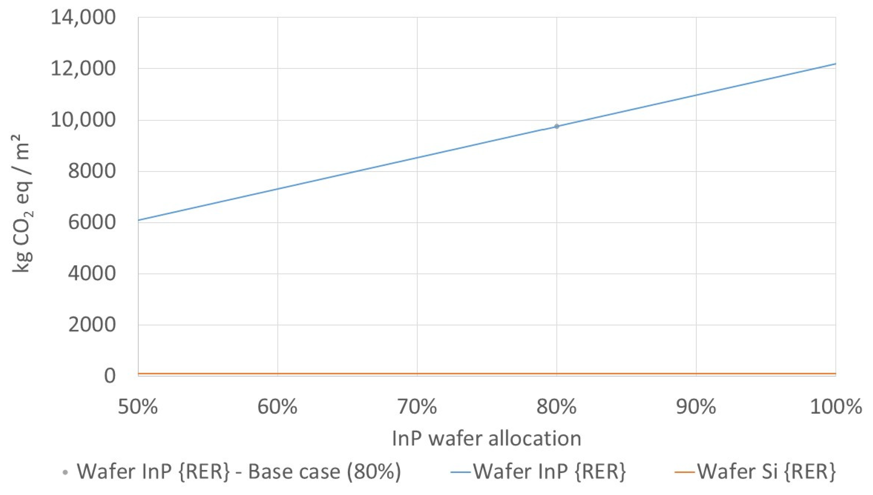
2.3.2. Sensitivity Analysis of LCA InP Wafer

A sensitivity analysis has been conducted to estimate the influence of allocation value on the climate change impact. In the base case, 80% of the environmental impacts are allocated to the wafers and 20% to the ingots’ extremities. The allocation is set between 50% and 100% to the InP wafer. Figure 3 shows that the climate change impact varies strongly with the allocation value. However, even with a lower allocation, the InP wafer still remains much more impactful than the silicon wafer (silicon estimated from [12] with European electrical mix, InP wafer calculated with European electrical mix). The thickness of the Si wafer used as a reference is 170 µm [12].
Figure 3. InP wafer carbon footprint depending on byproduct allocation.
A second limit in the model is the chemical production evaluation. Chemical names and quantities per chemical were not detailed by the industry for confidentiality reasons. According to [19], typical chemicals for InP wafer fabrication can be polishing agents, alkaline solution, hydrofluoric acid, sulfuric acid, hydrogen peroxide, and phosphoric acid. For the sensitivity analysis, two scenarios were elaborated. The best-case scenario replaces 358 kg of organic and inorganic chemicals with a probable chemical used in this industry that has the lowest impact per kg of chemical produced for each impact category (for example, sulfuric acid has the lowest impact for climate change). The worst-case scenario replaces organic and inorganic chemicals with the chemical that has the highest impact for each impact category per kg of chemical. The results in Figure 4 show that scenarios do not have significant influence on toxicity and ecotoxicity indicators. On climate change, variations of scenarios are more significant but stay below 20%.
Figure 4. Sensitivity analysis of chemical production (best case: chemical with lowest environmental impact, base case: 50% chemical organic, 50% chemical inorganic; worst case: chemical with higher environmental impact).
Thirdly, wastewater treatment has been modeled with the silicon factory wastewater treatment data from ecoinvent. As such, the modelling does not reflect the exact indium and phosphorus emissions contributing to eutrophication and freshwater ecotoxicity.
Finally, the data were not distinguished between wafer sizes. The data represent the average impact of the reference period of production with an average wafer area of 3869 mm2 and an average thickness of 512 µm. Energetic and material consumption should be more efficient with a larger and longer ingot. Generally speaking, there is a yield increase with larger diameter thanks to more optimum seed/tail material usage.

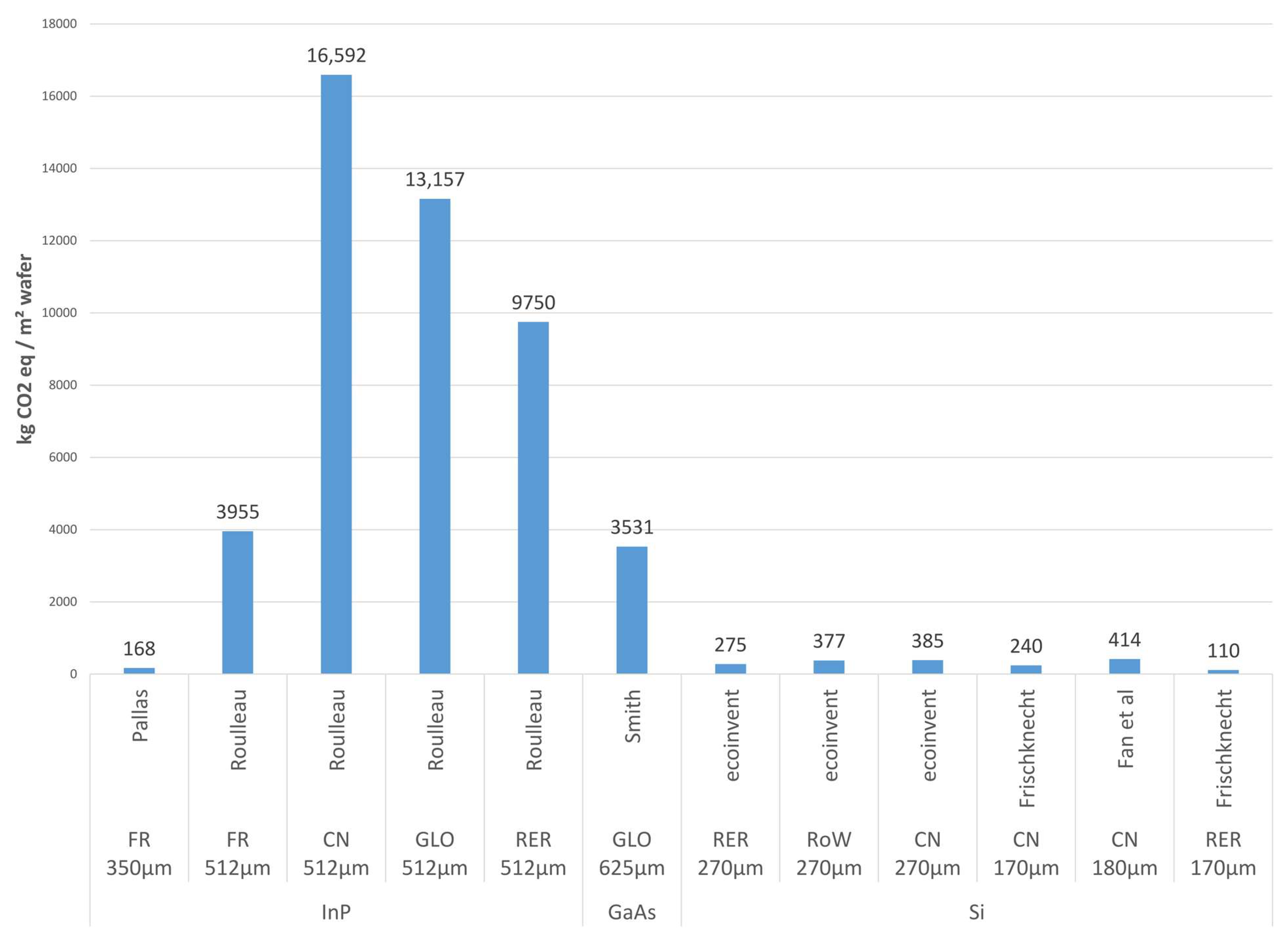
2.3.3. Comparison with III–V and Silicon Wafers

The previous LCA studies assessing the impacts of III–V wafers focused on photovoltaic applications. Smith evaluated the impacts of GaAs substrate and used it as a proxy for InP substrate impact, based on the similarity of III–V wafer manufacturing [17]. Meijer et al. evaluated the impact of GaAs wafer production [22]. Pallas estimated the environmental impacts of InP wafers by including only indium and phosphide extraction and adding electricity consumption for ingot melting [13]. Climate change results of wafer fabrication impact per m2 from different studies are compared in Figure 5 (Roulleau: current study, Pallas [13], Smith [17], ecoinvent, Frischknecht [12] adapted with electrical mix, Fan et al. [11]).
Figure 5. Comparison of greenhouse gas emissions for the production of III–V and silicon wafers with French (FR), Chinese (CN), global (GLO), European (RER), Rest of World (RoW) electricity mixes [11,12,13,17].
It can be seen that the electricity mix has a huge influence on GHG emissions. In this study, the climate change impact of InP wafer production is multiplied by 4.2 if the production takes place in China instead of France.
Pallas [13] calculated the impact with only the raw materials indium and phosphide and the electricity consumption (93.9 kWh/m2 of wafer). According to industrial data collected for this study, the electricity consumption is 190 times higher, which results in a 24 times higher carbon footprint in this study.
Ecoinvent data rely on quite old literature data and consider a process yield of 55%, which seems underestimated. Moreover, some studies pointed to limits in the ecoinvent wafer inventory [3,4]. The most recent studies are Frischknecht [12] and Fan et al. [11] (2020 and 2021) for silicon wafers.
Despite variabilities of climate change impact between study sources (which can be explained by the place of production, differences in wafer diameter and thickness, data quality, etc.), III–V wafers have higher climate change impacts than silicon wafers. The impact reduction will increase with the maturity of the InP industry. InP is migrating towards 6″ for both transceiver and imager applications; InP is more and more used in CMOS fabs, and it creates multiple opportunities to have more efficient material usage (recycling, access to standardized and automated wafering equipment…). One should also consider that a reduction in impact (by wafer), which can be achieved with higher-volume production, may lead to an absolute increase in impacts, with more wafers being produced.

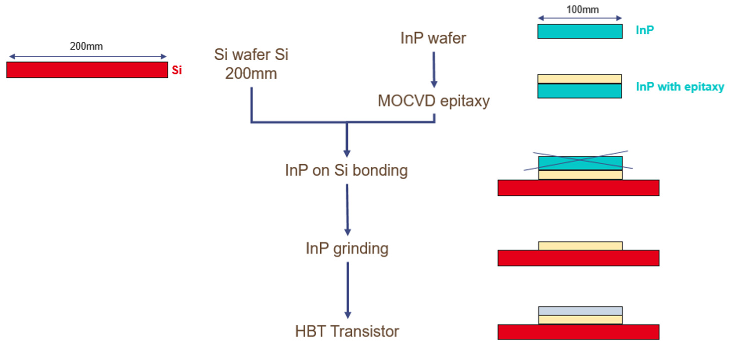
2.4. HBT InP Fabrication

2.4.1. System Description and Scope

The goals of this Life Cycle Assessment are to quantify the environmental impacts of InP-HBT transistor electronic component manufacturing and identify the main contributors along the fabrication chain. The functional unit is “production of InP-HBT transistor technology on a 200 mm diameter Si wafer”. For instance, InP HBT technology can provide radio frequency performance such as high-frequency radio signals of 10–12 dBm, with power added efficiency (PAE) of 38% for the transistor alone at 170 GHz [23].
This technology is still at an early stage of development; therefore, in order to demonstrate the electrical performance of the transistor, a transistor flow is realized on a 200 mm diameter Si wafer, as described in Figure 6. To achieve this demonstration, a 100 mm diameter InP substrate is bonded on a 200 mm diameter Si substrate. Most of the InP substrate is removed to keep only a thin layer of 1 µm on the Si substrate. This way of proceeding would not be industrialized because a lot of InP substrate is lost and the wafer area is underutilized (100 mm vs. 200 mm). Research is ongoing towards new ways to build InP transistors on Si wafers in order to allow their production at a large scale. These new ways are still in the early development stage and not included in this study [7,8]. The InP on silicon bonding and InP grinding are not included in the study because it would not be the final industrial process, as mentioned above.
Figure 6. InP HBT fabrication flow. Life cycle assessment for InP-BHT only includes the III–V MOCVD epitaxy step and the HBT transistor step.
In this part of the study, the LCA system boundary only includes the III–V MOCVD epitaxy step and InP-HBT transistor fabrication steps (Figure 6). The MOCVD of III–V layers is performed in a 300 mm epitaxy tool that is compatible with a variety of substrates, including 100 mm diameter InP substrates, and 200 mm and 300 mm Si substrates. InP-HBT transistor fabrication is performed on a 200 mm Si substrate. It includes here front-end-of-line (FEOL) for the active part of the device (emitter, contact) and does not include back-end-of-line (BEOL) for the metallic connections. BEOL can vary depending on the targeted integration and has already been studied separately by the authors [10].
The use, distribution, and end-of-life phases are not included because the complete electronic system is not yet developed.
The reference flow is “production of InP-HBT transistor technology on a 200 mm diameter Si wafer: epitaxy and FEOL”. The FEOL manufacturing flow of the HBT transistor based on III–V semiconductors and compatible with Si-CMOS consists of a succession of main technological building blocks, as described in Figure 7. After processing of the Emitter/Base Junction, the base contact is formed using a damascene-based approach. These steps are then repeated at the collector level, after the base contact isolation mesa has been produced and access has been enabled to the semiconductor layer of the collector/base junction. The three metal terminals that make up the transistor’s contacts are then connected to the future metal links at the back-end level using standard CMOS technology contact processes (component isolation brick, deposition of metal lines). In the configuration of an RF amplification circuit, another level of metal lines should be considered.
Figure 7. InP HBT FEOL process flow succinct description.

2.4.2. Life Cycle Inventory of InP Transistor Fabrication

Process steps are realized in a cleanroom that requires specific temperature, humidity and pressure conditions. A certain number of process steps are needed: chemical mechanical polishing (8), metal or dielectric deposition (20), dry etching (25), metalorganic chemical vapor deposition (MOCVD) epitaxy (1), photolithography, wet cleaning and wet etching (24) and wet or dry stripping (54). In our facility, at CEA-Leti, one step corresponds to one wafer processed on one piece of equipment, except for photolithography, where two pieces of equipment are used (one for insolation, the other for the rest of the steps). Several technological steps considered in this study (early R&D stage process flow) are not necessary in an industrial configuration where the production of electronic circuits is optimized. Consequently, it will be possible to reduce the number of photolithography masks considered here, given that some levels used for the recognition or creation of alignment marks of the E-Beam lithography levels are only needed in the context of our research and technological development. Each of these levels also includes plasma etching and in situ and wet stripping steps in order to prepare the wafers for the following process steps. Also, a high number of stripping steps are applied due to specific cleaning steps for III–V surfaces, and further optimization could decrease the number of cleaning steps. A more industrial process flow would require a reduced number of process steps.
Inventory data are collected for each process step with a bottom-up or a top-down collection method (Figure 8).
Figure 8. Data collection methodology.
At the cleanroom level, consumption of energy (electricity, natural gas) and cooling water for air handling (temperature, humidity, purity) are calculated from annual CEA-Leti cleanroom consumption data allocated with process time and surface of the equipment [24]. At the process level, deionized water, process gas, metals, and liquid chemicals are collected by interviewing the equipment engineer (collecting process time and flow of each input). Electricity, nitrogen, compressed air, and vacuum consumptions for the equipment are based on the top-down method, allocated with the number of pieces of equipment connected and process time. For the epitaxy, water, chemical, and electricity consumptions are collected at the process level by interviews with experts [25,26]. Input datasets for the four types of water used have been created by adapting ecoinvent datasets for softened or ultrapure water production with in-house data (water origin; French electricity mix, yield when known), as listed in Table 2.
In this study, the following outputs were inventoried: emissions of fluorinated gases into the air and emissions of liquid effluents into the water (Figure 8). Fluorinated gases and N2O with high global warming potential are often used in deposition and etching processes. The equipment using these gases is connected to abatement systems in order to remove these gases. Consumptions of abatement systems are estimated based on technical datasheets of abatement systems (consumption of methane, oxygen, nitrogen, and water for abatement systems). Final air emissions of fluorinated gases are calculated based on an emission model based on the Intergovernmental Panel on Climate Change (IPCC) guidelines: Tier 2b without combustion, which gives an average utilization factor of process gas in equipment and destruction removal efficiency coefficient [27]. Finally, wastewater treatment consumptions and emissions to water are collected annually and allocated by m3 of wastewater treated. CEA-Leti cleanroom disposes of three drains for wastewater treatment: acido-basic effluent drain, fluorhydric drain, and solvent tank. Regarding the solvents (such as isopropanol, EKC265™, acetone, and ethanol), 73% is collected and incinerated with energy valorization; it was measured that 17% is directly emitted to the air, and the 10% is also considered as emitted to the air. The fluorhydric effluent drain collects >1% fluorhydric acid solutions and liquid waste such as phosphoric acid, HCl, and HNO3. The fluorhydric effluent wastewater is treated with flocculent, lime and coagulant to precipitate sludge that will be treated and landfilled. The liquid is redirected to the acido-basic drain that is pH-neutralized with acid and soda. The three wastewater treatments have been modeled, with, in terms of inputs, the specific chemicals and other products required in a period of time and, in terms of outputs, the final emissions in the environment in this same period of time. Then, dividing those inputs and outputs by the volume treated allows the creation of an allocation by volume unit. For each process, the same volume of water and chemicals consumed by the process was considered as output to one or several of the three wastewater treatments.
Several hypotheses are made either to estimate the process flow in an industrial context or to simplify the study:
-
Metrology, characterization, and specific decontamination steps related to the R&D environment are removed from the analysis.
-
It is also supposed that the wafer occupancy rates in equipment are maximized.
-
Two scenarios have been elaborated: a first scenario without abatement systems and a second scenario with abatement systems on each piece of equipment that uses process gases that are greenhouse gases.
-
The transistor flow is assumed to have 100% of process yield; no losses are considered.
The following items are excluded from the study: equipment manufacturing (missing data and impacts supposed to be compensated by the high number of uses and long lifetime of the equipment); equipment gas consumption during idle phase (missing data on uptime/idle time and assumed to be negligible in an industry production line); consumables needed for the operators in cleanroom environment such as plastic gloves, masks, working cleanroom clothes, safety shoes; research impact during working time (considered out of scope); lithography mask fabrication (impacts supposed to be compensated by the high number of uses in a high volume of production); BEOL and packaging of the die (missing data).
Table 2 gathers the consumption of energy, water, chemicals and process gas for the flow for one 200 mm wafer processed. The consumption of metals was also included in the study but is not reported in the table. Photolithography steps last longer than other steps on average (around 10 min per wafer). Therefore, with allocation rules, photolithography steps consume more electricity for the process and cleanroom and water for the cleanroom. Deionized water during the process is mostly consumed during chemical mechanical polishing, wet cleaning, and stripping steps. Chemicals are mostly consumed during chemical mechanical polishing (slurry) and during wet cleaning steps (for wet etching).
Table 2. Life cycle inventory (Inputs) for the following functional unit (FU): production flow of InP-HBT transistor technology on a 200 mm diameter Si wafer: epitaxy and FEOL. * Many different chemicals are used in semiconductor processing, and the non-exhaustive list of inventories includes ammonia, anhydrous, liquid {RER}|market for ammonia, anhydrous, liquid|Cut-off, U; hydrochloric acid, without water, in 30% solution state {RER}|market for hydrochloric acid, without water, in 30% solution state|Cut-off, U; hydrogen fluoride {RER}|market for hydrogen fluoride|Cut-off, U; hydrogen peroxide, without water, in 50% solution state {RER}|market for hydrogen peroxide, without water, in 50% solution state|Cut-off, U; isopropanol {RER}|market for isopropanol|Cut-off, U; sulfuric acid {RER}|market for sulfuric acid|Cut-off, U. ** Many different gases are used in semiconductor processing, and the non-exhaustive list of inventories includes argon, liquid {RER}| argon production, liquid|Cut-off, U; chlorine, gaseous {RER}|market for chlorine, gaseous|Cut-off, U; helium {GLO}|market for helium|Cut-off, U; hydrogen, liquid {RER}|market for hydrogen, liquid|Cut-off, U; oxygen, liquid {RER}|market for oxygen, liquid|Cut-off, U; NF3 and SiH4 modelled according to [28]; nitrogen, liquid {RER}|market for nitrogen, liquid|Cut-off, U; nitrous oxide {GLO}|market for nitrous oxide|Cut-off, U; sulfur hexafluoride, liquid {RER}|market for sulfur hexafluoride, liquid|Cut-off, U; trifluoromethane {GLO}|market for trifluoromethane|Cut-off, U.
Step FamilyUnit (/FU)EpitaxyEtchingDepositionPhotolithographyStrippingWet Etching/CleaningChemical Mechanical PolishingTotal for the Flow Per WaferEcoinvent Inventory (v3.9.1) (In Italics When Inventory Has Been Modified)
Number of steps 12520165488132
Electricity consumption
of the equipment
during process
kWh695102611211134Electricity, low voltage {FR}|market for electricity, low voltage|Cut-off, U
Electricity consumption
for cleanroom
kWh279204319318139Electricity, low voltage {FR}|market for electricity, low voltage|Cut-off, U
Natural gas consumption
for cleanroom
kWh312420214Heat, district or industrial, natural gas {Europe except Switzerland}|heat production, natural gas|Cut-off, U
Total energy consumptionkWh9916327332530287
Deionized water consumption
during process
L-1-173-124199CEA Water, deionized {FR}|water production, ultrapure|Cut-off, U
Ultrapure water consumption
for equipment
L-588931149183CEA Water, ultrapure {FR}|water production, ultrapure|Cut-off, U
Softened water for cleanroomL11481881758CEA_Water, completely softened {FR}|water production|Cut-off, U
Cooling water for cleanroomL7722725681240543845083988CEA_Water, harvested from rainwater {FR}|rainwater harvesting|Cut-off, U
Total water consumptionL7832825841349655866884428
Liquid chemical consumption
for process
L0.02--1.61.86.99.520*
Process gas consumptionm30.40.102.370.020.010.180.003**

2.4.3. Results of Life Cycle Impact Assessment of InP Transistor

Environmental Indicator Selection
Normalization and weighting methods bring out a selection of environmental indicators to investigate based on an 80% contribution to the single score. The indicators are the following: climate change (kg CO2 eq); resource use, fossils (MJ); resource use, minerals and metals (kg Sb eq); ionizing radiation (kBq U-235 eq); photochemical ozone formation (kg NMVOC eq); particulate matter (disease inc); and ecotoxicity, freshwater (CTUe) (Figure 9). Those indicators are selected for the contribution analysis. Climate change; resource use, fossils; resource use, minerals and metals; and ecotoxicity, freshwater were also identified as relevant environmental indicators for the InP wafer (Figure 2). Ionizing radiation, photochemical ozone formation, and particulate matter are specific to the InP HBT fabrication.
Figure 9. Family steps contributing to the relevant environmental indicators, with abatement systems on 6 pieces of equipment, for the functional unit (FU): production flow of InP-HBT transistor technology on a 200 mm diameter Si wafer: epitaxy and FEOL.
Contribution Analysis per Family Steps
The selected environmental indicators’ contribution per family step is represented in Figure 9 with the number of steps in each family of processes. On the climate change indicator, contribution analysis shows that epitaxy has the highest contribution compared to the number of steps. Indeed, epitaxy consumes a lot of electricity for the process (69 kWh), and the step is long, thus consuming a lot of electricity (27 kWh) and gas (3 kWh) for cleanroom infrastructure use. Deposition and dry etching steps use process gases that are fluorinated or greenhouse gases such as SF6, NF3, CHF3, C4F8, CF4, or N2O. They have a global warming potential (GWP) thousands of times higher than CO2 (the highest two being SF6 with a GWP of 24,300 and NF3 with 17,400) and a lifetime in the atmosphere also thousands of times higher than CO2 (the highest one being CF4 with 50,000 years). The climate change method evaluates a lifetime horizon of 100 years. Abatement systems enable a reduction in direct greenhouse gas emissions by cracking the fluorinated gases used in the process.
Chemical mechanical polishing (CMP) steps show lots of impact on all indicators, mainly because of slurry production. As slurry composition is often confidential, a proxy for the LCA model has been defined based on the safety datasheet.
Photolithography steps last longer than other steps on average (around 10 min per wafer). Therefore, photolithography steps have a big contribution to resource use (fossils and minerals and metals) due to electricity consumption.
Stripping steps have a low impact compared to the high number of steps. Stripping steps do not last long (around 1 min per wafer), and equipment works in batches of 25 wafers, so stripping steps have low electricity consumption.

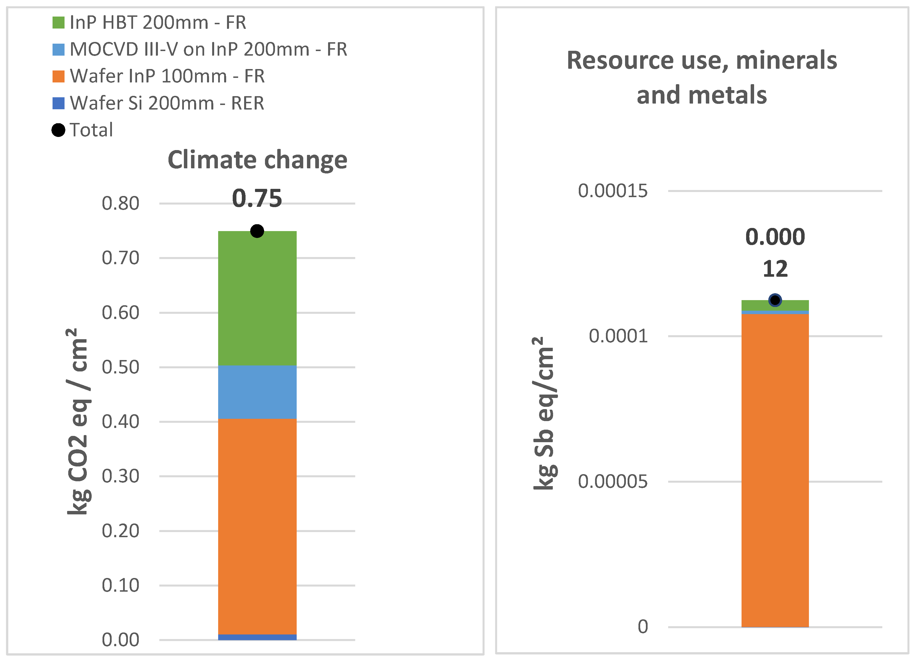
2.4.4. Results for the Flow (Including Epitaxy and HBT Transistor)

Results in Table 3 show that with abatement systems, climate change impact is reduced by 53% in comparison with a scenario without abatement systems. However, eutrophication; resource use, fossils; and water use are increased by 19%, 14%, and 132%, respectively, due to the increase in water consumption for the abatement system. The use of abatement systems has not had a significant influence on other indicators (resource use, fossils; resource use, minerals and metals; and ecotoxicity, freshwater).
Table 3. Results for the selected indicators for the functional unit (FU): production flow of InP-HBT transistor technology on a 200 mm diameter Si wafer: epitaxy and FEOL.
Contribution Analysis per Inventory
Inventory contributions are calculated for the flow with abatement systems (Table 4). Hotspots are reported when they contribute to above 5% of total impact for the entire flow. It should be noted that French electricity consumption is a hotspot for many impact categories, even though French electricity is low-carbon. The climate change impact of French electricity comes from coal, natural gas and petrol used in the French electrical mix (71% of nuclear considered in the inventory ecoinvent 3.9.1). Fossil resource use and freshwater ecotoxicity electricity impact comes from uranium. Mineral and metal resource use originates from uranium and copper used for the electricity distribution network. Freshwater eutrophication is derived from coal and lignite use in the electrical mix. Besides electricity consumption, water production is also a great contributor to several impact categories: water use (ultrapure water and deionized water require higher quantities of water).
Table 4. Main hotspots per environmental indicators for the following functional unit (FU): production flow of InP-HBT transistor technology on a 200 mm diameter Si wafer: epitaxy and FEOL, with abatement systems on 6 pieces of equipment.
From Wafer to Transistor
In this part, the results of the InP HBT transistor FEOL fabrication steps (with abatement system) are normalized by cm2 for a 200 mm diameter wafer and compared to 200 mm Si and 100 mm InP wafer fabrication, also normalized by cm2 (Figure 10). For a better visualization, the impact of the epitaxy step is here reported separately from the InP HBT transistor and normalized for a 200 mm diameter wafer. As mentioned before, it should be noted that the MOCVD of III–V layers is performed in a 300 mm epitaxy tool that is compatible with a variety of substrates, including 100 mm diameter InP substrates, and 200 mm and 300 mm Si substrates. Therefore, the epitaxy impacts by cm2 are higher when performed on 100 mm substrates and can be reduced by performing the epitaxy on a larger substrate size. The normalization is performed by division of the results for a wafer by wafer area, without taking into account any slicing loss (edge, trench) or yield loss.
Figure 10. Climate change impact, from wafer to transistor fabrication. InP HBT 200 mm stands for the following functional unit (FU): FEOL production flow of InP-HBT transistor technology on a 200 mm diameter Si wafer, with abatement systems. MOCVD III–V on InP 200 mm is the epitaxy step for the production of this InP-HBT transistor technology on a 200 mm diameter Si wafer. A 170 µm thick 200 mm diameter Si wafer is modeled according to reference [12] adapted with the European electrical mix (Frischknecht RER in Figure 5). A 512 µm thick 100 mm diameter InP wafer is modeled according to Section 2.2 of this study (Roulleau FR in Figure 5).
On the climate change indicator (Figure 10), the impact from the InP wafer fabrication accounts for approximately half of the total impact, followed by InP HBT transistor fabrication and III–V epitaxy, while the Si wafer has little impact. Si wafers used for semiconductor manufacturing are usually 3–5× thicker than the ones used for photovoltaic manufacturing [12], so the impact by cm2 should increase; even so, their impact on climate change would stay small in comparison with the other contributors. InP small wafer size leads to high impacts by cm2. The impacts of InP HBT transistor fabrication and MOCVD epitaxy on climate change are due to electricity consumption. Vanhouche et al. reported higher values with 2.46 kgCO2eq/cm2 of InP HBT technology with NRE, with significant contribution from the epitaxy step, but used a high CO2 electricity mix [8].
Most of the impact on the resource use, minerals and metals indicator comes from the InP wafer fabrication. These results show that, for a given number of devices, new ways to build larger InP wafers or InP devices on larger Si wafers have the potential to improve the impacts by cm2. An overall absolute reduction in impact will only be achieved with a limited increase or reduction in the production volume, in order to avoid rebound effects, with more wafers being produced.

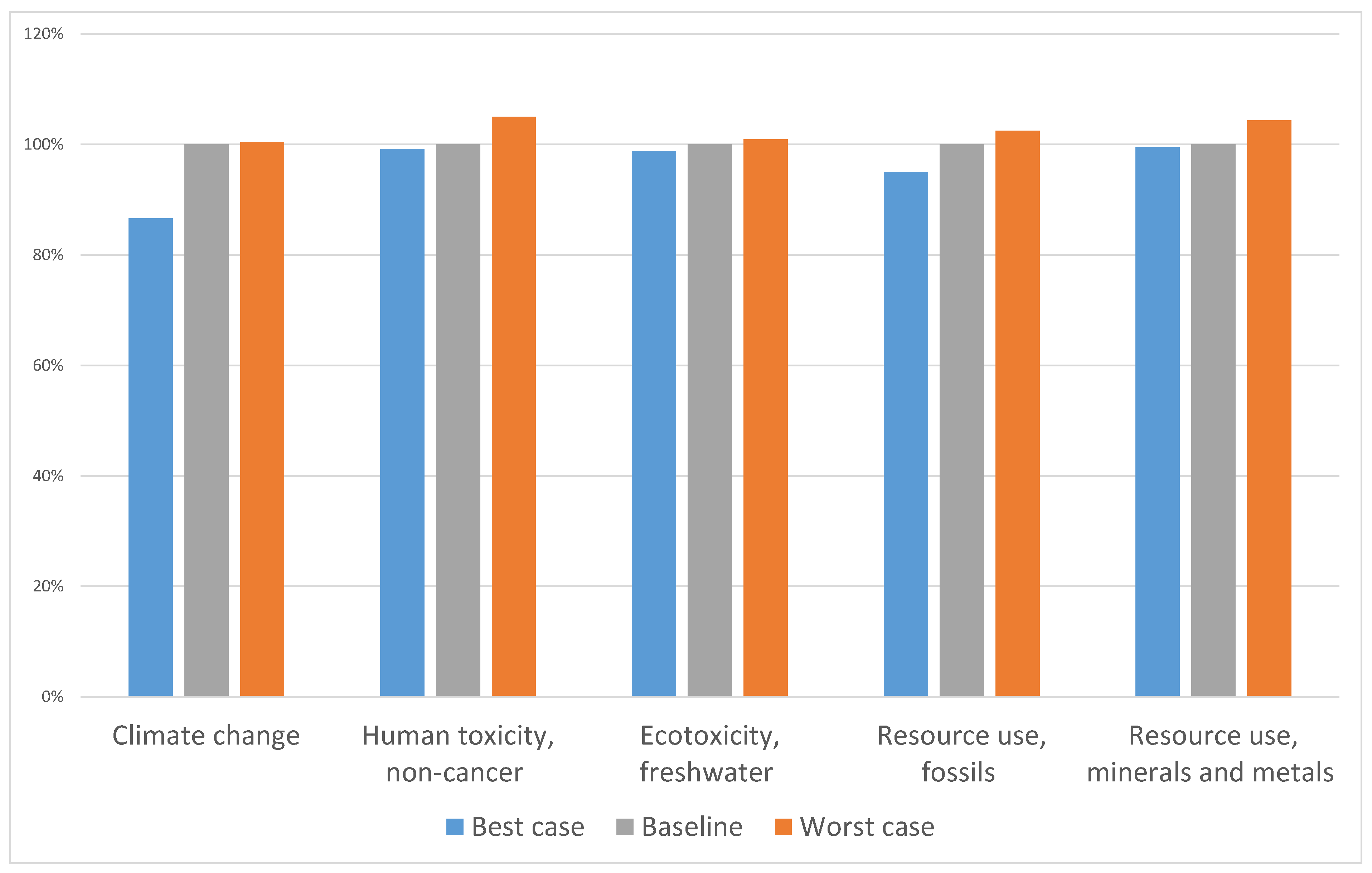
2.4.5. Sensitivity Analysis of LCA InP-HBT Transistor Fabrication

Limits of LCA Model
Certain assumptions were made in this LCA. The data were collected from an R&D center, which is tailored for small-scale production and not optimized for large-scale manufacturing. For example, the allocation of global cleanroom consumption uses the process duration, which means that all equipment consumes the same amount of electricity per second. Actually, each piece of equipment has a different electricity consumption per second of process, depending in the process temperature (sometimes above 1000 °C), vacuum requirement, etc. Moreover, some process steps are not yet completely stabilized and optimized in terms of process duration, temperature, pressure, quantity of process gas, liquid chemicals, etc. The process flow is also not finalized; some choices of equipment, thickness of layer, and deposition methods are not completely fixed. All conditioning and autocleaning of equipment has been modeled as imagined in an industrial environment. Interviewing industry experts would be valuable to further validate and strengthen this information.
Some chemicals have been modeled, such as slurry and etching chemicals, based on safety datasheets. Two organic chemicals for the epitaxy step have been excluded either because few pieces of information were found on their synthesis or because the impact was inconsistent. The impact of energy required for chemical synthesis and chemical purification at the required purity degree for semiconductor manufacturing could have a significant impact and should be better modeled.

3. Deployment Scenario

The Environmental Footprint method (EF3.1) indicator for resource use, minerals and metals evaluates the resource depletion with a ratio between resource extraction and ultimate resource based on the concentration in earth’s crust, compared to the antimony reference (Abiotic Depletion Potential ultimate reserves, in kg Sb eq). This indicator allows us to quantify the relative contribution of a product system to the depletion of mineral resources [29].
Ahead of resource depletion, critical metals are defined by potentially unstable supply and economic importance. Indium is a byproduct of zinc (95%) and copper and tin (5%) mines. Its production, therefore, strongly depends on primary production, which makes availability hard to evaluate. The production also depends on the element content in the mine deposit and on the economic interest of refining this byproduct [30]. Only 35% of zinc refineries are equipped to recover indium [31]. According to [32], few industries have their own production chain integrated from zinc extraction to indium extraction. In most of cases, mineral extraction and metal refinery take place in a different country. Supply risk methods allow for the evaluation of potential mineral resource availability issues for a product system related to short-term geopolitical and socio-economic aspects. Recommended supply risk methods include ESSENZ (Integrated Method to Assess Resource Efficiency) or GeoPolRisk (Geopolitical Risk Supply) [29]. In the ESSENZ, one of the geopolitical and socioeconomic constraints to take into account is demand growth.
In this study, we propose a deployment scenario to estimate the amount of indium required for InP HBT transistors in the global rollout of 6G applications, based on several assumptions. Our scenario is informed by recent work from the ETSI THz standardization group, which focuses on establishing the technical framework for the development and standardization of THz communications for future wireless networks. The growing interest in higher frequency bands is driven by the increasing demand for greater bandwidth and lower latency to support critical applications [33]. This trend is particularly evident in research on 6G technologies, which are expected to be ready for initial deployment after 2030. The vast bandwidth available in THz frequency bands allows for exceptionally high data rates and helps mitigate spectrum scarcity. Additionally, the unique propagation characteristics of THz signals enable advanced features such as precise sensing and imaging capabilities. These attributes of THz communication pave the way for innovative use cases and offer potential solutions to emerging challenges that future 6G systems must address. Some of these challenges involve functionalities not currently supported by cellular networks, such as precise sensing, mapping, and localization, while others involve entirely new use cases previously unsupported by existing communication technologies.
In our study, we explore three scenarios: the integration of THz capabilities into mobile phones, the incorporation of THz technology in access points, and the use of THz for high-speed Fixed Wireless Access (FWA) connections. For all these applications, beamforming is assumed, leading to the integration of multiple antennas and RF chains within the system [34]. Consequently, the number of InP devices scales with the antenna count, as detailed in Table 5.
Table 5. Calculation of indium quantities required for global deployment of 6G applications, with InP transistors produced on 100 mm InP substrates.
It is first assumed that the 6G deployment will extend over 10 years (which is the approximate time to change from one mobile generation to another mobile generation). As mobile phone replacement, typically 36 months, is not driven by communication technology but rather by phone add-ons (such as screens, operating systems, application support), we assume there will be a gradual device replacement over the first 10 years, which aligns with a linear increase in the number of devices. Thus, quantities of indium are calculated for a global deployment and then divided by 10 years of deployment. It is also assumed that all new phones will have InP components and that the indium is not recycled. It is important to emphasize that continuous mineral sourcing will be required beyond 10 years. While it can be assumed that, beyond a certain threshold of equipment deployment, recycling channels may emerge, the study does not account for developments occurring beyond this 10-year horizon. Finally, other applications under development, such as chip-to-chip connection and communication radar (Face ID), are not included in the calculation due to missing information about the future production.
With these hypotheses made, it is estimated that in ten years, 0.1% (396 tons) of the estimated In quantity in known mineral deposits (380 kt in 2017 [37]) would be consumed for 6G deployment with InP transistors produced on 100 mm InP substrates. The indium characterization factor for resource use, minerals and metals representing the extraction rate over reserves has increased from 6.9 × 10⁻³ to 2.3 × 10⁻¹ [38], which means that the impact of indium on the environment has increased, as assessed by the Abiotic Depletion Potential.
We estimated that 40 tons of indium would be needed annually, for ten years, to deploy 6G applications in the world with InP transistors produced on 100 mm InP substrates. This would represent 4.4% of global annual production of indium (2022 production: 897 tonnes per year [36]; average over the period 2016–2020: 845 tonnes per year [39]), which would be needed each year over the course of 10 years, a significant part of the 2022 production. The indium production may increase, as it has been continuously increasing since 1980 until 2015 [38]. Werner et al. suggested that in the event of a supply restriction, In capacity could be developed elsewhere, although there are numerous challenges in converting dormant resources into supply [37]. Indium is used in various applications such as flat screens (56%), welds (10%), thin film photovoltaics (CIGS, ITO, CdTe, and Si-amorphous) (8%), and batteries (5%) [31]. The deployment of these technologies will lead to an evolution of the indium market and potential competition for In supply. For instance, the high demand scenario for indium used in thin film CIGS photovoltaic technology (19 to 53 t/year in 2018 globally) can lead to an increase of up to 40 times in 2050 [40]. The increase in electronic devices can lead to an increase in this indium consumption (25 t/year in 2020 in France for all uses) by up to 5 times in 2050 for the high-demand scenario with high IoT deployment [14]. Expected long-term annual demand of indium ranges from 1000 to 9000 t, with a significant share for low-carbon technologies [41]. If all these technologies tend towards a high deployment scenario, indium supply will be at high risk.
The deployment of InP semiconductor technology will require, if deployed at large scale for 6G communication, based on current InP HBT technology on 4” InP substrates, a significant share of the annual indium production. This study highlights that material needs for the production of Information and Communication technologies (ICTs) might compete with the material needs for other applications such as flat panel displays or photovoltaic technology. An increase in indium extraction and production may also increase the associated environmental impacts.

4. Conclusions

In this study, we have assessed the environmental impacts of manufacturing commercially available InP wafers, which demonstrate higher impacts than Si wafers (Figure 5), mainly due to In 6N production and electricity consumption (Figure 2). We have evaluated the environmental impacts at an early stage of R&D of the InP heterojunction bipolar (HBT) transistor fabrication process on Si in order to help make better technological choices. Performing the III–V epitaxy on larger substrates, using abatement systems for fluorinated gases (Table 3), and reducing the number of process and photolithography steps (mask levels) should help to reduce the environmental impacts by wafer. Finally, the indium material requirements for a deployment of InP HBT technology for 6G application (on 4″ InP substrates) show that 4% of the current (2022) annual In production would be needed (Table 5). This highlights the potential benefits of developing alternative technologies (such as InP transistors on large Si wafers) regarding this issue. In conclusion, this study addresses the environmental impacts during manufacturing and material use and allows the identification of main hotspots and paths for decreasing these impacts by unit (by m2 or by wafer). However, relative improvement of the environmental impacts per unit might be associated with the opposite effect at the absolute level; with a high increase in production volume, the environmental impacts associated with manufacturing might increase globally (rebound effect).
Beyond the environmental impacts of manufacturing, it is important to bear in mind that the environmental impact of communication networks relies mostly on energy consumption during use [2]. Higher impacts of manufacturing might be associated with overall benefits, if allowing for significant improvement of the energy consumption during the use phase. However, the growth of mobile data usage and the expansion of mobile network sites may lead to an increase in energy consumption by telecommunication networks, as an average annual 5% increase was found by the ARCEP study on the environmental impacts of ICT in France [42]. These findings highlight that it is necessary to look at the full life cycle, including the use phase, with the deployment scenario in order to assess the environmental impacts of a new technology.

Author Contributions

Conceptualization, L.R., L.V., H.B. and L.D.C.; Methodology, L.R.; Formal analysis, L.R.; Investigation, L.R., D.M., L.C., J.-B.D. and A.D.; Writing—original draft, L.R., L.V., D.M., H.B. and J.-B.D.; Writing—review & editing, L.V.; Visualization, L.R. and L.V.; Supervision, L.V. and L.D.C.; Project administration, L.V. and H.B.; Funding acquisition, H.B. and L.D.C. All authors have read and agreed to the published version of the manuscript.

Funding

This work was supported by the French ANR, via Carnot funding.

Data Availability Statement

Most of the original contributions presented in this study are included in the article. Further inquiries can be directed to the corresponding author(s).

Acknowledgments

The authors wish to acknowledge Thierry Baron, Jérémy Moeyaert from CNRS-LTM for the data on the epitaxy process, CEA-Leti teams who contributed to the processes and LCI data collection, CEA-Leti eco-innovation team for the establishment of the LCA methodology adapted for CEA-Leti cleanrooms, Yannick Rivoira, Mélanie Alias, Mathilde Billaud and Elise Chaumat for reviewing the manuscript.

Conflicts of Interest

Author Didier Marsan was employed by the company inPACT. The remaining authors declare that the research was conducted in the absence of any commercial or financial relationships that could be construed as a potential conflict of interest.

References

  1. Freitag, C.; Berners-Lee, M.; Widdicks, K.; Knowles, B.; Blair, G.S.; Friday, A. The real climate and transformative impact of ICT: A critique of estimates, trends, and regulations. Patterns 2021, 2, 100340. [Google Scholar] [CrossRef]
  2. Freitag, C.; Berners-Lee, M.; Widdicks, K.; Knowles, B.; Blair, G.; Friday, A. The Climate Impact of ICT: A Review of Estimates, Trends and Regulations; Small World Consulting: Bailrigg, UK, 2020; p. 87. [Google Scholar]
  3. Pirson, T.; Delhaye, T.; Pip, A.; Le Brun, G.; Raskin, J.-P.; Bol, D. The Environmental Footprint of IC Production: Meta-Analysis and Historical Trends. In Proceedings of the ESSDERC 2022—IEEE 52nd European Solid-State Device Research Conference (ESSDERC), Milan, Italy, 19–22 September 2022; pp. 352–355. [Google Scholar] [CrossRef]
  4. Clément, L.-P.P.-V.P.; Jacquemotte, Q.E.S.; Hilty, L.M. Sources of variation in life cycle assessments of smartphones and tablet computers. Environ. Impact Assess. Rev. 2020, 84, 106416. [Google Scholar] [CrossRef]
  5. Arushanyan, Y.; Ekener-Petersen, E.; Finnveden, G. Lessons learned—Review of LCAs for ICT products and services. Comput. Ind. 2014, 65, 211–234. [Google Scholar] [CrossRef]
  6. Urteaga, M.; Griffith, Z.; Seo, M.; Hacker, J.; Rodwell, M.J.W. InP HBT Technologies for THz Integrated Circuits. Proc. IEEE 2017, 105, 1051–1067. [Google Scholar] [CrossRef]
  7. Ghyselen, B.; Navone, C.; Martinez, M.; Sanchez, L.; Lecouvey, C.; Montmayeul, B.; Servant, F.; Maitrejean, S.; Radu, I. Large-Diameter III–V on Si Substrates by the Smart CutProcess: The 200 mm InP Film on Si Substrate Example. Phys. Status Solidi A 2022, 219, 2100543. [Google Scholar] [CrossRef]
  8. Vanhouche, B.; Rolin, C.; Boccardi, G.; Boakes, L.; Winckel, L.V.; Ragnarsson, L.-Å.; Wambacq, P.; Parvais, B. Sustainability Analysis of Indium Phosphide technologies for RF applications. In Proceedings of the DATE2023, Antwerp, Belgium, 17–19 April 2023. [Google Scholar]
  9. Oliveira, A.; Valorge, O.; Dubarry, C.; Roelens, Y.; Zaknoune, M.; Lugo-Alvarez, J. RF Performances and De-Embedding Techniques of Passive Devices in 3D Homogeneous Integration at Sub-THz. In Proceedings of the 2023 53rd European Microwave Conference (EuMC), Berlin, Germany, 19–21 September 2023; IEEE: Berlin, Germany, 2023; pp. 616–619. [Google Scholar] [CrossRef]
  10. Roulleau, L.; Vauche, L.; Valorge, O.; Dubarry, C.; Di Cioccio, L. Comparative life cycle assessment of hybrid bonding and copper pillar die-to-wafer 3D integrations for sub-THz applications. In Proceedings of the European Microwave Week 2023, Berlin, Germany, 18–19 September 2023. [Google Scholar] [CrossRef]
  11. Fan, M.; Yu, Z.; Ma, W.; Li, L. Life Cycle Assessment of Crystalline Silicon Wafers for Photovoltaic Power Generation. Silicon 2021, 13, 3177–3189. [Google Scholar] [CrossRef]
  12. Frischknecht, R.; Itten, R.; Sinha, P.; de Wild-Scholten, M.; Zhang, J.; Heath, G.A.; Olson, C. Life Cycle Inventories and Life Cycle Assessments of Photovoltaic Systems; National Renewable Energy Laboratory (NREL): Golden, CO, USA, 2015. [Google Scholar] [CrossRef]
  13. Pallas, G.; Vijver, M.G.; Peijnenburg, W.J.G.M.; Guinée, J. Life cycle assessment of emerging technologies at the lab scale: The case of nanowire-based solar cells. J. Ind. Ecol. 2020, 24, 193–204. [Google Scholar] [CrossRef]
  14. Ollion, L.; Drapeau, P.; Boztepe, L.; Villers, S.D.; Bouyer, G.; Vergari, L.; Fangeat, E.; Kergaravat, O. Etude des Besoins en Métaux dans le Secteur Numérique—Recueil de Fiches; ADEME: Angers, France, 2024. [Google Scholar]
  15. ISO 14040:2006; Environmental Management—Life Cycle Assessment—Principles and Framework. International Organisation for Standardisation (ISO): Geneva, Switzerand, 2006.
  16. Pant, R.; Zampori, L. Suggestions for Updating the Product Environmental Footprint (PEF) Method; Publications Office of the European Union: Luxembourg, 2019. [Google Scholar]
  17. Smith, B.L. Development and Life Cycle Assessment of Advanced-Concept III–V Multijunction Photovoltaics. Ph.D. Thesis, Rochester Institute of Technology, Rochester, NY, USA, 2018. [Google Scholar]
  18. Oda, O. Compound Semiconductor Bulk Materials and Characterizations; World Scientific Publishing Co., Pte Ltd.: Singapore, 2007. [Google Scholar]
  19. Okita, K. Indium Phosphide Substrate Manufacturing Method, Epitaxial Wafer Manufacturing Method Indium Phosphide Substrate, and Eptaxal Wafer. U.S. Patent 8,487,409, 16 July 2013. [Google Scholar]
  20. InPACT—The Indium Phosphide substrates (InP) Specialist. Available online: https://www.inpactsemicon.com/p_process.php (accessed on 23 August 2023).
  21. ISO 14044; Environmental Management—Life Cycle Assessment—Requirements and Guidelines. International Organisation for Standardisation (ISO): Geneva, Switzerland, 2006.
  22. Meijer, A.; Huijbregts, M.A.J.; Schermer, J.J.; Reijnders, L. Life-cycle assessment of photovoltaic modules: Comparison of mc-Si, InGaP and InGaP/mc-Si solar modules. Prog. Photovolt Res. Appl. 2003, 11, 275–287. [Google Scholar] [CrossRef]
  23. Ciabattini, F.; Hamzeloui, S.; Arabhavi, A.M.; Ebrahimi, M.; Ostinelli, O.; Bolognesi, C.R. G-Band Large-Signal Characterization of InP/GaAsSb DHBTs with Record 38% Power Added Efficiency at 170 GHz. In Proceedings of the 2024 19th European Microwave Integrated Circuits Conference (EuMIC), Paris, France, 23–24 September 2024; IEEE: Piscataway, NJ, USA, 2024; pp. 335–338. [Google Scholar] [CrossRef]
  24. Lopes Barbosa, J.C.; Enyedi, V.; Di Cioccio, L.; Zwolinski, P.; Largeron, C. Développement d’une méthodologie de collecte de données pour l’Analyse du Cycle de Vie (ACV) dans l’environnement de la recherche. In Proceedings of the Axelera, Online, 25 October 2022. [Google Scholar]
  25. Ghyselen, B.; Darras, F.-X.; Mourey, O.; Navone, C.; Sanchez, L.; Nardo, C.D.; Crobu, C.; Toselli, L.; Rousset, B.; Dechamp, J.; et al. Large Diameter Epi-Ready InP on Si (InPOSi) Substrates. In Proceedings of the Digests of 2023 International Conference on Compound Semiconductor Manufacturing Technology, Orlando, FL, USA, 15–18 May 2023; Volume 86, pp. 223–231. [Google Scholar] [CrossRef]
  26. Besancon, C.; Vaissiere, N.; Dupré, C.; Fournel, F.; Sanchez, L.; Jany, C.; David, S.; Bassani, F.; Baron, T. Epitaxial Growth of High-Quality AlGaInAs-Based ActiveStructures on a Directly Bonded InP-SiO2 /Si Substrate. Phys. Status Solidi A 2020, 217, 1900523. [Google Scholar] [CrossRef]
  27. 2019 Refinement to the 2006 IPCC Guidelines for National Greenhouse Gas Inventories; Electronics Industry Emissions; s.l.:Intergovernmental Panel on Climate Change: Geneva, Switzerland, 2019; Volume 3, Chapter 6.
  28. Jungbluth, N.; Stucki, M.; Flury, K.; Frischknecht, R.; Büsser, S. Life Cycle Inventories of Photovoltaics; ESU-services Ltd., Fair Consulting in Sustainability: Uster, Switzerland, 2012. [Google Scholar]
  29. Berger, M.; Sonderegger, T.; Alvarenga, R.; Bach, V.; Cimprich, A.; Dewulf, J.; Frischknecht, R.; Guinée, J.; Helbig, C.; Huppertz, T.; et al. Mineral resources in life cycle impact assessment: Part II—recommendations on application-dependent use of existing methods and on futuremethod development needs. Int. J. Life Cycle Assess. 2020, 25, 798–813. [Google Scholar] [CrossRef]
  30. Barreau, B.; Hossie, G.; Lutfalla, S. Approvisionnements en Métaux Critiques. 2013. Available online: https://strategie.archives-spm.fr/cas/system/files/2013-07-10-metaux-na03.pdf (accessed on 25 September 2023).
  31. BRGM Fiche de Synthèse sur la Criticité des métaux—L’indium. Available online: https://www.mineralinfo.fr/sites/default/files/documents/2020-12/fichecriticiteindium170921.pdf (accessed on 9 January 2023).
  32. Chalmin, P.; Jégourel, Y. Les Marchés Mondiaux—CyclOpe “Le Monde D’hier”; Economica: London, UK, 2022. [Google Scholar]
  33. TeraHertz (THz) ETSI Industry Specification Group (ISG). TeraHertz Modeling (THz); Identification of Use Cases for THz Communication Systems; ETSI, ETSI GR THz 001 V1.1.1 (2024-01). 2024. Available online: https://www.etsi.org/deliver/etsi_gr/THz/001_099/001/01.01.01_60/gr_THz001v010101p.pdf (accessed on 23 September 2024).
  34. Rasilainen, K.; Phan, T.D.; Berg, M.; Pärssinen, A.; Soh, P.J. Hardware Aspects of Sub-THz Antennas and Reconfigurable Intelligent Surfaces for 6G Communications. IEEE J. Select. Areas Commun. 2023, 41, 2530–2546. [Google Scholar] [CrossRef]
  35. Seto, K.C.; Güneralp, B.; Hutyra, L.R. Global forecasts of urban expansion to 2030 and direct impacts on biodiversity and carbon pools. Proc. Natl. Acad. Sci. USA 2012, 109, 16083–16088. [Google Scholar] [CrossRef] [PubMed]
  36. Mineral Commodity Summaries 2023; U.S. Geological Survey: Reston, VA, USA, 2023.
  37. SCREEN Criticality Factsheet of Indium. SCREEN2 EU HORIZON EUROPE PROJECT, Update 2023. Available online: https://scrreen.eu/wp-content/uploads/2023/12/SCRREEN2_factsheets_INDIUM-update-.pdf (accessed on 3 January 2025).
  38. van Oers, L.; Guinée, J.B.; Heijungs, R. Abiotic resource depletion potentials (ADPs) for elements revisited—Updating ultimate reserve estimates and introducing time series for production data. Int. J. Life Cycle Assess 2020, 25, 294–308. [Google Scholar] [CrossRef]
  39. Werner, T.T.; Mudd, G.M.; Jowitt, S.M. The world’s by-product and critical metal resources part III: A global assessment of indium. Ore Geol. Rev. 2017, 86, 939–956. [Google Scholar] [CrossRef]
  40. Watari, T.; Nansai, K.; Nakajima, K. Review of critical metal dynamics to 2050 for 48 elements. Resour. Conserv. Recycl. 2020, 155, 104669. [Google Scholar] [CrossRef]
  41. European Commission. Joint Research Centre. Raw Materials Demand for Wind and Solar PV Technologies in the Transition Towards a Decarbonised Energy System; European Commission: Brussels, Belgium, 2020. [Google Scholar]
  42. Perasso, E.L.; Vateau, C.; Domon, F.; Aiouch, Y.; Chanoine, A.; Corbet, L.; Drapeau, P.; Ollion, L.; Vigneron, V.; Prunel, D.; et al. Evaluation Environnementale des Equipements et Infrastructures Numériques en France. ADEME and ARCEP. January 2022. Available online: https://librairie.ademe.fr/ (accessed on 22 October 2024).
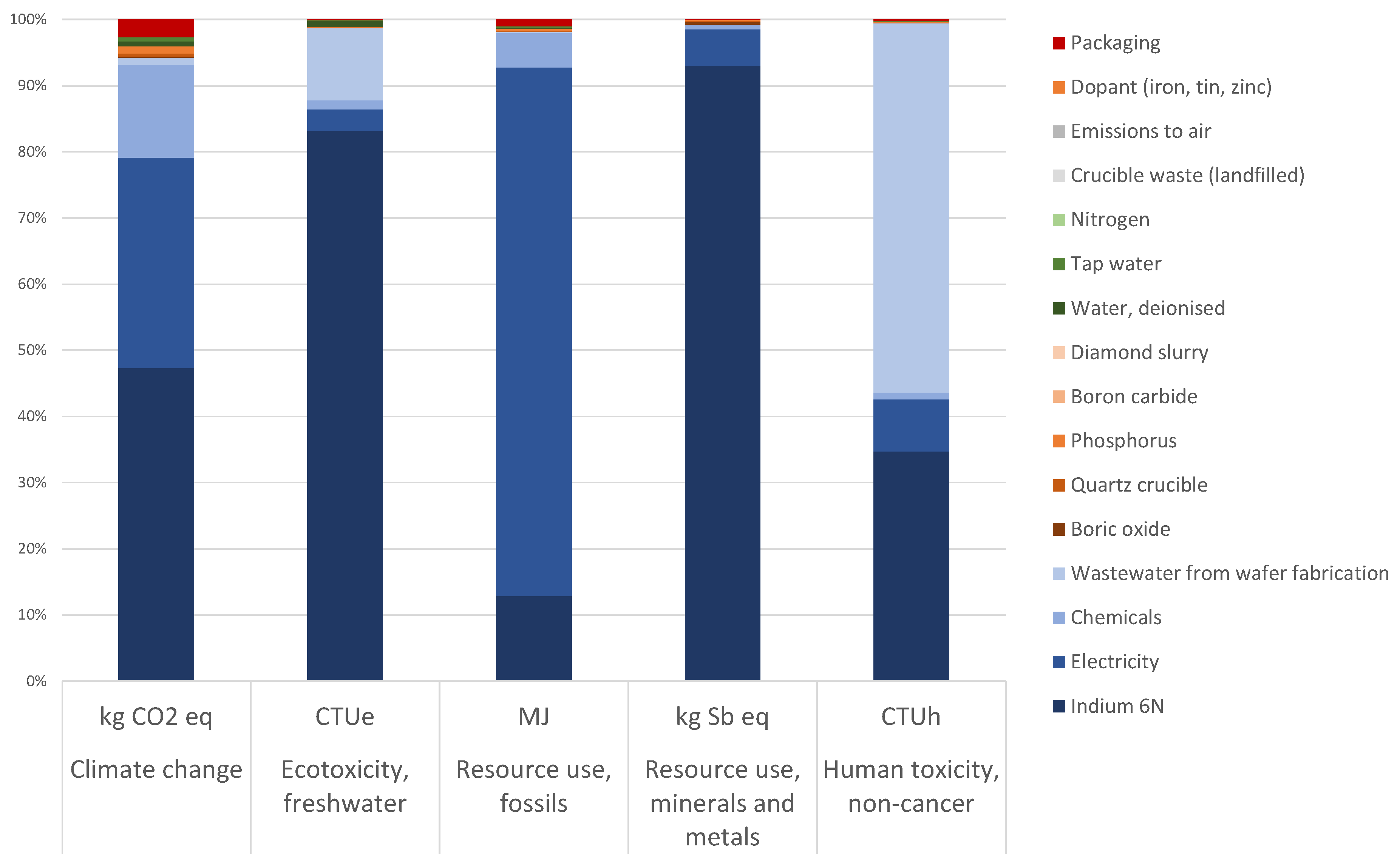
Disclaimer/Publisher’s Note: The statements, opinions and data contained in all publications are solely those of the individual author(s) and contributor(s) and not of MDPI and/or the editor(s). MDPI and/or the editor(s) disclaim responsibility for any injury to people or property resulting from any ideas, methods, instructions or products referred to in the content.

Article Metrics

Citations

Article Access Statistics

Multiple requests from the same IP address are counted as one view.