Article

DFT Investigation of a Direct Z-Scheme Photocatalyst for Overall Water Splitting: Janus Ga2SSe/Bi2O3 Van Der Waals Heterojunction

Aix-Marseille University, UFR Sciences, IM2NP, CNRS, 13013 Marseille, France
*
Author to whom correspondence should be addressed.
Materials 2025, 18(7), 1648; https://doi.org/10.3390/ma18071648
Submission received: 7 February 2025 / Revised: 20 March 2025 / Accepted: 26 March 2025 / Published: 3 April 2025

Abstract

:
Constructing van der Waals heterojunctions with excellent properties has attracted considerable attention in the field of photocatalytic water splitting. In this study, four patterns, coined A, B, C, and D of Janus Ga2SSe/Bi2O3 van der Waals (vdW) heterojunctions with different stacking modes, were investigated using first-principles calculations. Their stability, electronic structure, and optical properties were analyzed in detail. Among these, patterns A and C heterojunctions demonstrate stable behavior and operate as direct Z-scheme photocatalysts, exhibiting band gaps of 1.83 eV and 1.62 eV. In addition, the suitable band edge positions make them effective for photocatalytic water decomposition. The built-in electric field across the heterojunction interface effectively inhibits electron-hole recombination, thereby improving the photocatalytic efficiency. The optical absorption coefficients show that patterns A and C heterojunctions exhibit higher light absorption intensity than Ga2SSe and Bi2O3 monolayers, spanning from the ultraviolet to visible range. Their corrected solar-to-hydrogen (STH) efficiencies are 13.60% and 12.08%, respectively. The application of hydrostatic pressure and biaxial tensile strain demonstrate distinct effects on photocatalytic performance: hydrostatic pressure preferentially enhances the hydrogen evolution reaction (HER), while biaxial tensile strain primarily improves the oxygen evolution reaction (OER). Furthermore, the heterojunctions exhibited enhanced optical absorption across the UV-visible spectrum with increasing hydrostatic pressure. Notably, a 1% tensile strain results in an improvement in visible light absorption efficiency. These results demonstrate that Ga2SSe/Bi2O3 heterojunctions hold great promise as direct Z-scheme photocatalysts for overall water splitting.

1. Introduction

The pursuit of renewable and eco-friendly energy solutions is essential in light of the growing global energy crises and environmental concerns [1,2]. The photocatalytic decomposition of water to produce hydrogen has emerged as a pivotal area of scientific research, owing to its potential to generate clean and renewable hydrogen energy [3,4,5]. However, several obstacles hinder the development of efficient photocatalysts, including appropriate band gap alignment [6,7], effective charge separation [8,9], and good chemical stability [9,10].
In the past few years, two-dimensional materials have gained significant attention in photocatalysis due to their distinctive physicochemical properties [11,12]. Among these, transition metal chalcogenides (TMCs) have emerged as particularly effective photocatalytic materials owing to their tunable band gaps [13,14], high carrier mobility [15,16], and substantial specific surface areas [15,17]. Metal oxides are also efficient photocatalysts for water decomposition to produce hydrogen, thanks to their excellent light absorption and electron-hole pair generation capabilities [18,19]. Gallium selenide sulfide (Ga2SSe), for example, demonstrates considerable promise for photocatalytic applications due to its unique electronic structure, which confers upon it remarkable visible light absorption properties [20]. R. da Silva et al. demonstrated that the Janus Ga2SSe monolayer has a stable structure, an indirect band gap, and low exciton binding energy. These features, along with efficient electron-hole separation and unique electronic alignment, make Ga2SSe highly suitable for photocatalytic water splitting and hydrogen generation [21]. Concurrently, bismuth oxide (Bi2O3), a well-established metal oxide photocatalyst, exhibits remarkable activity in photocatalytic reactions. P. Riente et al. explored the structure and electronic properties of α-Bi2O3 and β-Bi2O3 using first principles methods, and their findings aligned well with experimental data. Their photocatalytic activity arises from their narrowed band gaps, Bi 6s—O 2p hybridized orbitals, and red-shifted light absorption edges. Their optical properties highlight the potential of these polymorphs for efficient water splitting [22].
Single-component photocatalysts offer numerous beneficial properties. However, their performance is often hindered by a common issue: rapid photogenerated carrier recombination, which significantly limits photocatalytic efficiency [23]. To address this issue, designing heterojunctions is a promising approach to improving photocatalytic performance. By combining complementary materials, heterojunctions can effectively promote charge separation [24,25], inhibit recombination [26,27], and extend the range of light absorption [28,29]. Notably, van der Waals (vdW) heterojunctions, consisting of diverse two-dimensional (2D) materials, enhance photocatalytic water decomposition by improving interfacial interactions and overcoming the limitations of monolayer catalysts. R. Kumar et al. employed first principles methods to demonstrate that the C2N/WS2 vdW heterojunction exhibits improved photocatalytic performance for water splitting as a result of its type-II band alignment, efficient charge separation, and high visible light absorption. The heterojunction’s dual-layer mechanism facilitates both the oxidation and reduction of water, and thermodynamic analysis confirms its potential for efficient hydrogen generation. This study underscores the significant potential of heterojunction photocatalysis and can be a basis for developing next-generation 2D photocatalysts [30].
Heterojunctions, which can be directly employed in photocatalysis, include type-II and direct Z-scheme heterojunctions, both of which effectively separate photogenerated carriers and enhance redox reactions [31,32]. Van der Waals (vdW) heterojunctions consisting of 2D TMCs and metal oxides have shown significantly improved performance in photocatalytic water decomposition [13,33]. Recent research reveals that integrating 2D H-TiO2 with MoS2 or WS2 leads to the formation of vdW heterojunctions with enhanced stability, direct band gaps, and superior visible light absorption, bringing significant advancements in technologies related to photocatalytic and solar energy conversion [34]. The type-II ZnO/Ga2SSe and ZnO/GaSe heterostructures exhibit favorable bandgap characteristics and band edge alignments for photocatalytic water splitting. Notably, the ZnO/Ga2SSe heterostructure with sulfur vacancies demonstrates spontaneous hydrogen evolution reaction activity, achieving a substantial solar-to-hydrogen (STH) efficiency of 25.05% [35]. Similarly, the Z-scheme ZrS2/Ga2SSe van der Waals heterojunction, featuring an indirect bandgap of 1.33 eV, benefits from its optimized band structure and built-in electric field, which facilitate efficient electron transfer and significantly enhance photocatalytic performance. The heterojunction achieves an STH efficiency of 10.93% under a compressive strain of −6% [36]. The Bi2O3/MoS2 p-n heterojunction photocatalyst, with strong light-harvesting ability and efficient charge-carrier separation, exhibits superior visible-light-driven performance with a hydrogen conversion efficiency reaching up to 10 μmol h−1g−1 [37]. Additionally, the S-scheme TiO2/Bi2O3 heterojunction, with its optimized interface structure, reduces the migration distance of charge carriers, enhancing photocatalytic water-splitting performance for hydrogen production and displaying an H2 generation rate of 12.08 mmol h−1g−1 [38]. The systematic study of the electronic structure and photocatalytic performance of the various heterojunctions mentioned above provides valuable insights for guiding our research. This prompts an intriguing question: can we combine the high-performance Janus structure Ga2SSe with the metal oxide Bi2O3 to construct a novel Ga2SSe/Bi2O3 heterojunction for exploring its potential in photocatalysis?
In this work, the electronic properties, energy band alignment, and photocatalytic properties of the Ga2SSe/Bi2O3 heterojunction were systematically investigated using density-functional theory (DFT) approaches. The charge transfer within the heterojunction was analyzed through charge density difference and Bader charge calculations. To evaluate the photocatalytic potential of the heterojunction, its optical absorption properties and solar-to-hydrogen efficiency were also calculated. In parallel, we investigated the effects of hydrostatic pressure and biaxial strain on the photocatalytic performance of heterojunctions, focusing on their electronic properties and optical absorption characteristics. These results offer meaningful understanding of the photocatalytic mechanism of the Janus Ga2SSe/Bi2O3 heterojunction, highlighting the potential of this class of heterojunctions for hydrogen production through photocatalysis.

2. Computational Methods

In this study, all the calculations were carried out by means of density functional theory (DFT) [39,40] within the framework of the Vienna Ab initio Simulation Package (VASP) [41,42,43,44]. The Perdew–Burke–Ernzerhof (PBE) functional within the generalized gradient approximation (GGA) was utilized as an exchange-correlation functional [45], and the projector-augmented wave (PAW) method was employed to describe ion–electron interactions [46,47]. A plane-wave basis set was used with a cutoff energy of 450 eV and the first Brillouin zone was sampled with a k-point grid of 9 × 9 × 1. To minimize interactions between periodic images, a vacuum layer of 20 Å was implemented along the z-direction. Convergence thresholds were set to 10−5 eV for total energy and 0.05 eVÅ−1 for atomic forces, respectively. The DFT-D3 method proposed by Grimme [48] was utilized to account for van der Waals interactions. To accurately predict electronic structures, correct the underestimated band gaps by GGA functionals, and calculate optical properties, the Heyd–Scuseria–Ernzerhof (HSE06) hybrid functional, incorporating 20% exact exchange energy, was adopted [49,50]. Ab initio molecular dynamics (AIMD) simulations were conducted to assess thermal stability. The AIMD simulations, spanning 4 ps with a time step of 1 fs, were performed at a temperature of 300 K, regulated by the Nosé–Hoover thermostat. Additionally, Bader charge analysis [51] was performed to evaluate atomic charge distributions.

3. Results and Discussion

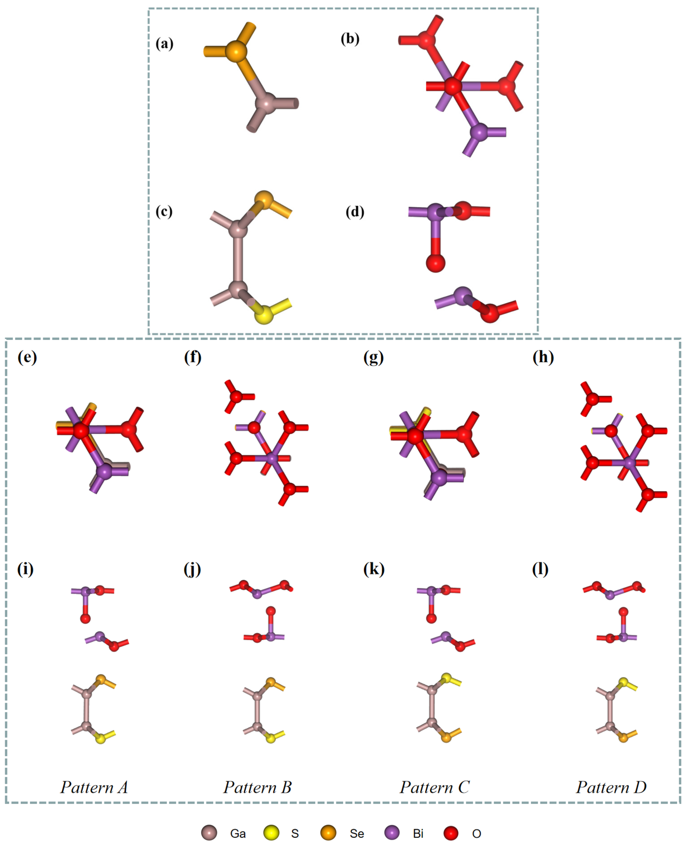
3.1. Structural Configurations and Stability of the Heterojunction

The of Ga2SSe and Bi2O3 monolayers were obtained by cleaving the hexagonal Ga2SSe and Bi2O3 crystals along the (001) direction. The optimized structures of Ga2SSe and Bi2O3 are presented in Figure 1a–d. The lattice constants for Ga2SSe and Bi2O3 monolayers were calculated to be 3.71 Å and 3.87 Å, which align well with earlier reports [52,53].The small lattice mismatch of 4.2% between Ga2SSe and Bi2O3 suggests their capability to establish a stable heterojunction within the two-dimensional plane. Owing to the structural asymmetry of the Ga2SSe and Bi2O3 monolayers, four distinct heterojunction configurations were constructed. These configurations vary based on the chemical element positioned on either side of the van der Waals gap, as shown in Figure 1e–l, and are designated as patterns A, B, C, and D. The electronic energy band structures of Ga2SSe and Bi2O3 monolayers were calculated using the HSE06 hybrid functional, as shown in Figure 2a,b. The results indicate that both Ga2SSe and Bi2O3 monolayers are indirect bandgap semiconductors, with bandgaps of 2.95 eV and 2.76 eV. These findings align with previous reports [54,55].
The four different heterojunctions were optimized, resulting in the lattice parameters (with a = b), interfacial distances (d), and interfacial energies (Eint) gathered in Table 1. The stability of the different heterojunctions can be estimated using the following equation:
E i n t = E G a 2 S S e / B i 2 O 3 E G a 2 S S e E B i 2 O 3
where EGa2SSe/Bi2O3 represents the total energy of the heterojunction, while EGa2SSe and EBi2O3 correspond to the total energies of the individual monolayers. Negative interfacial energies indicate stabilizing interactions between the two monolayers of the heterojunctions, and the lower the Eint value is, the more stable the formed heterojunction is.
The results in Table 1 suggest the feasible formation of all four heterojunctions, and that patterns A and C are more stable than patterns B and D. These two most stable patterns exhibit the smallest interlayer distances, which could be ascribed to strong interactions between oxygen and sulfur (or selenium) atoms, due to their proximity in the considered configuration (see Figure 1).
The band gaps of heterojunctions B and D (0.32 eV and 0.30 eV, respectively) clearly do not meet the requirements for photocatalytic water splitting (see below for band gap values). Therefore, their thermal stability was not further analyzed using molecular dynamics simulations. In the subsequent analysis, ab initio molecular dynamics (AIMD) simulations were performed to further investigate the thermal stability of heterojunctions A and C. The simulations were conducted using a supercell configuration of 3 × 3 × 1, with the temperature fixed at 300 K. Figure 3a,b illustrate the fluctuations in the total energy of the pattern A and C heterojunctions. These figures reveal that the total energy fluctuations for both heterojunctions are significant during the initial 500 fs. However, as time extends to 4000 fs, the fluctuations stabilize at weak levels. Given this stabilization of the fluctuations and the fact that the structures of heterojunctions A and C have not been drastically modified by the end of the simulation, we can conclude that these heterojunctions are thermally stable at an ambient temperature [56,57].

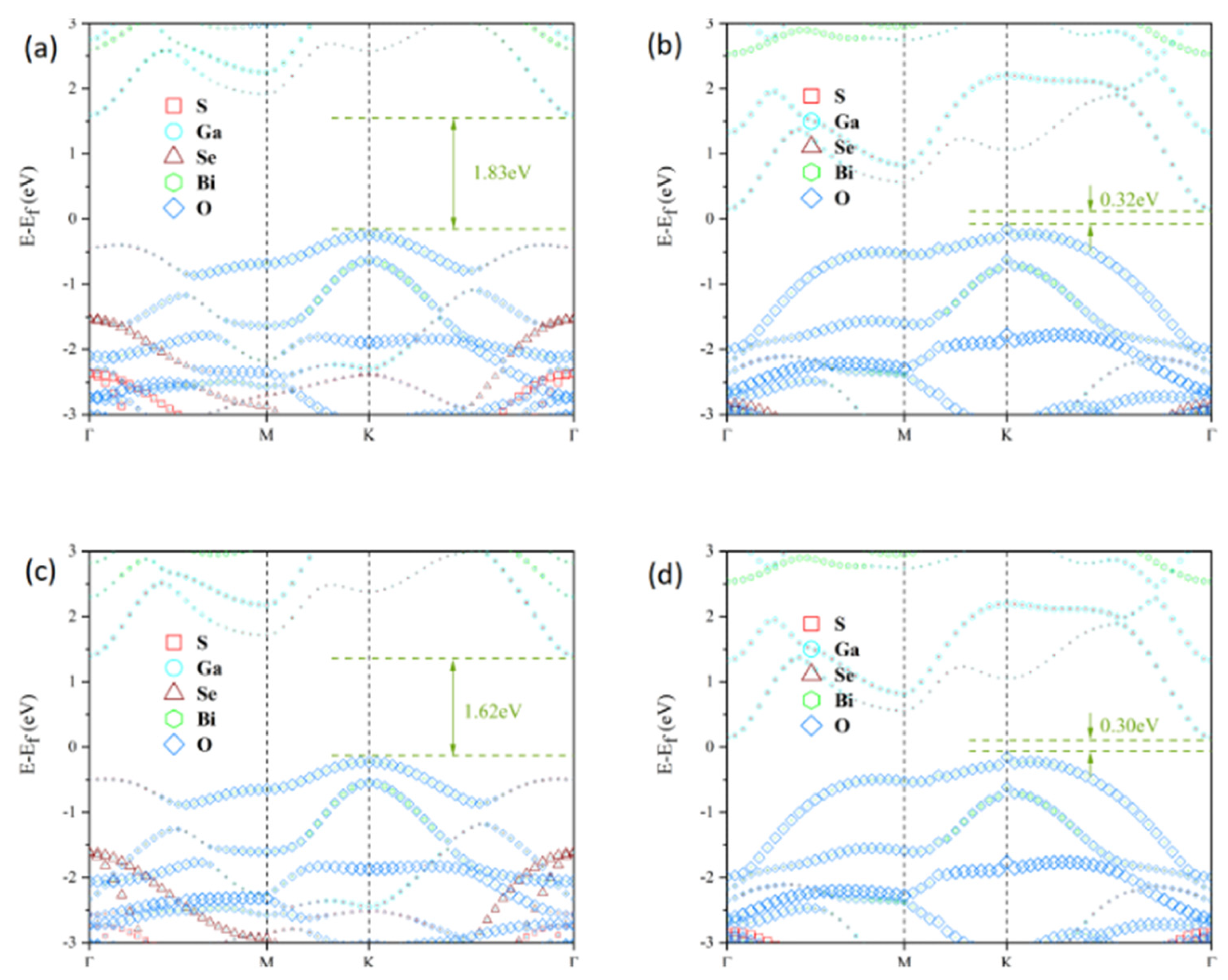
3.2. Electronic Properties

To investigate the electronic properties of the Janus Ga2SSe/Bi2O3 vdW heterojunctions, atom-projected band structures were computed using the HSE06 functional, as shown in Figure 4a–d. In all patterns (A–D), the valence band maximum (VBM) is positioned at the K point, whereas the conduction band minimum (CBM) appears at the Γ point. Therefore, all four heterojunction patterns exhibit indirect bandgaps, with values of 1.83 eV, 0.32 eV, 1.62 eV, and 0.30 eV, respectively. We observe that the bandgap width can be correlated to the van der Waals interlayer distance and to the nature of the atoms that are closest to each other across the vdW gap. Indeed, for the heterojunctions A and C, the closest atoms are selenium and oxygen (pattern A) and sulfur and oxygen (pattern C). These patterns lead to the smallest interlayer distances (2.533 Å and 2.396 Å) and largest bandgap widths (1.83 eV and 1.62 eV). Additionally, the larger the interlayer distance the larger the bandgap energy is. For the heterojunctions B and D, the nearest atoms across the vdW gaps are gallium and selenium (pattern B) and gallium and sulfur (pattern D). The bandgap energies are rather small and quite similar, with values 0.32 eV and 0.30 eV. Incidentally, we observe the same similarity for the vdW gap distances (3.587 Å and 3.586 Å). The smallness of the bandgap energies observed for these heterojunctions is probably related to the presence of the gallium near the vdW gaps, which provides a small metallic character to the structures. The modulation of the electronic structure of heterojunctions has already been reported in the literature [58,59,60,61]. Additional analysis demonstrates that the VBM and CBM of the four heterojunction patterns stem from the Bi2O3 and Ga2SSe layers, respectively. This suggests that all the heterojunctions exhibit a type-II band alignment, which effectively hinders the recombination of photogenerated electron-hole pairs. Notably, the bandgaps of pattern B and D heterojunctions do not satisfy the minimum energy threshold of 1.23 eV for photocatalytic water splitting. Therefore, the following analysis primarily focuses on the pattern A and C heterojunctions. Furthermore, the three-dimensional charge density difference (CDD) was computed to analyze charge transfer and separation at the interfaces of the pattern A and C heterojunctions, as illustrated in Figure 5a,d. The yellow regions indicate charge accumulation, whilst the cyan regions denote charge depletion. The CDD was calculated using the following equation [62]:
Δ ρ = ρ G a 2 S S e / B i 2 O 3 ρ G a 2 S S e ρ B i 2 O 3
where ρGa2SSe/Bi2O3, ρGa2SSe, and ρBi2O3 correspond to the total charge density of the heterojunction and the individual monolayers, respectively. Analysis of the CDD reveals that the Ga2SSe layer transfers electrons to the Bi2O3 layer. Bader charge analysis indicates that about 0.0343 |e| for pattern A and 0.0294 |e| for pattern C are transferred from the Ga2SSe layer to the Bi2O3 layer at the heterojunction interface. This indicates that the charge transfer mechanism in pattern A and C heterojunctions corresponds to that of a direct Z-scheme heterojunction. These findings resemble the electron transfer behavior reported in Janus MoSSe/Ga2SSe vdW heterojunctions [20].
In order to determine the direction of the electric field and charge transfer, the electrostatic potential of the pattern A and pattern C heterojunctions was analyzed along the z-axis [63]. The findings are presented in Figure 5b,e. Owing to the difference in vacuum energy levels, the pattern A and pattern C heterojunctions exhibit electrostatic potential differences of 0.727 eV and 0.538 eV, respectively. It is clear that the Bi2O3 layer possesses a lower potential than the Ga2SSe layer, causing electrons to migrate from the Ga2SSe layer to the Bi2O3 layer. This is further validated by the planar-averaged electron density difference, as depicted in Figure 5c,f. The planar-averaged electron density difference was determined by integrating the in-plane CDD, following the equation [62]:
Δ ρ z = ρ G a 2 S S e / B i 2 O 3 d x d y ρ G a 2 S S e d x d y ρ B i 2 O 3 d x d y
where ∫ρGa2SSe/Bi2O3dxdy, ∫ρGa2SSedxdy, and ∫ρBi2O3dxdy represent the charge densities of the heterojunction and the two monolayers, respectively, integrated over the xy plane. The transfer of electrons from the Ga2SSe layer to the Bi2O3 layer results in the establishment of an internal electric field directed from the Bi2O3 layer to the Ga2SSe layer at the heterojunction interface. This built-in electric field direction is beneficial to the separation of photogenerated electron-hole pairs.

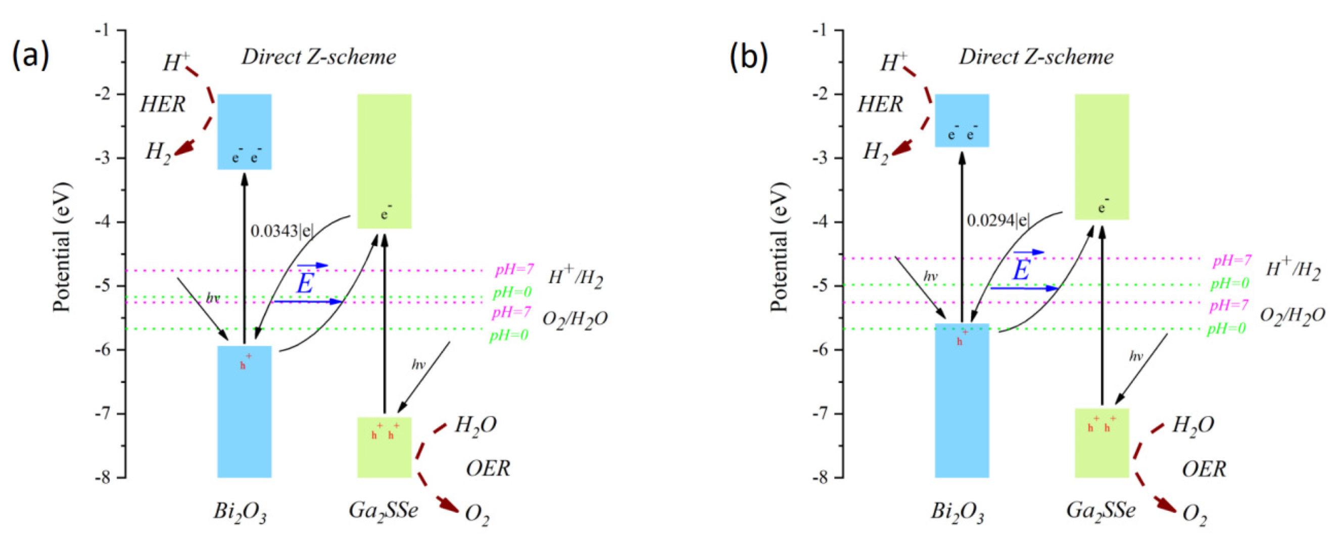
3.3. Photocatalytic Water-Splitting Properties

For effective water decomposition, photocatalytic materials must meet two essential requirements: (1) a band gap exceeding 1.23 eV, and (2) redox potentials of water positioned within the band gap [64]. More precisely, the conduction band minimum (CBM) should be greater than the water reduction potential, while the valence band maximum (VBM) must be less than the oxidation potential. According to literature [65], the water reduction and oxidation potentials at pH = 0 are −5.67 eV and −4.44 eV, respectively. To evaluate the potential of the pattern A and C heterojunctions for photocatalytic water splitting, the band edge positions were determined using the following equations:
E V B M = I = χ 0.5 E g
E C B M = A = E V B M + E g
where I, A, χ, and Eg denote the ionization energy, electron affinity, absolute electronegativity, and band gap of the respective material, respectively. These parameters are critical for determining the VBM and CBM positions and evaluating whether the patterns A and C heterojunctions meet the necessary conditions for photocatalytic activity. Generally, conventional photocatalytic materials must possess a band gap exceeding 1.23 eV to promote water-splitting reactions. However, following a novel methodology introduced by Li et al. [66], the band gap threshold for polar materials is revised as Eg > 1.23−ΔΦ eV, where ΔΦ represents the static potential difference, with ΔΦ > 0.
The standard potential expressions for the H+/H2 and O2/H2O couples in aqueous solutions as a function of the pH can be expressed as follows [35,65]:
E H + / H 2 = 4.44 + 0.059 p H
E O 2 / H 2 O = 5.67 + 0.059 p H
At a pH of zero, the water reduction and oxidation potentials are −5.67 eV and −4.44 eV, respectively. As the pH increases to 7, these potentials shift to −5.26 eV and −4.03 eV. Based on the method outlined by Li et al. [66], the corrected band edge positions of the patterns A and C heterojunctions were calculated and are illustrated in Figure 6. For the pattern A heterojunction, the band edge position meets the water redox potentials at both pH = 0 and pH = 7. In contrast, the band edge position of the pattern C heterojunction satisfies the water redox potentials only at pH = 7. These results indicate that pattern A can promote both the oxygen evolution reaction (OER) and hydrogen evolution reaction (HER) in acidic and neutral environments, while pattern C is limited to a pH range of 1.2 to 7.

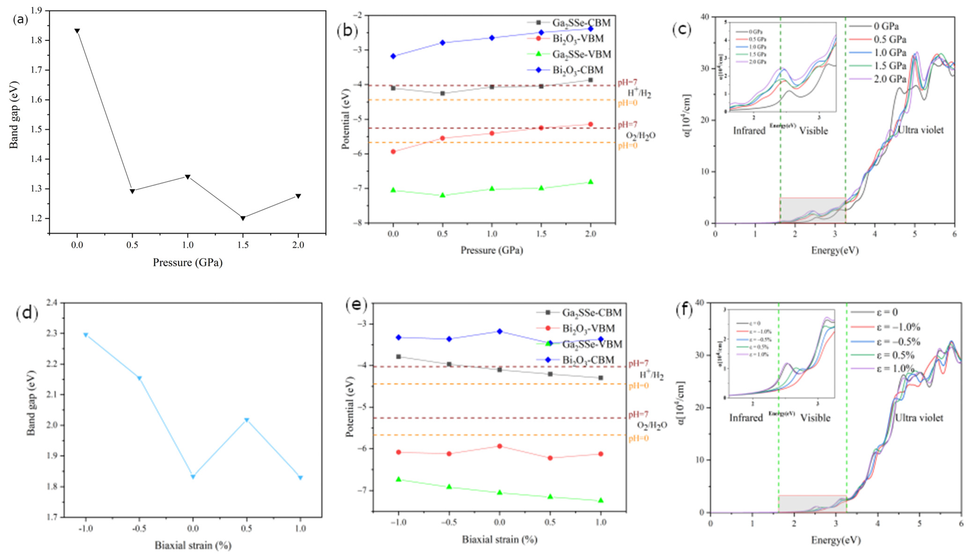
3.4. Optical Properties

To determine the optical properties of the Ga2SSe/Bi2O3 vdW heterojunctions and the isolated Ga2SSe and Bi2O3 monolayers, the dielectric function (ε) [67] was calculated, and the absorption coefficient (α) was derived accordingly [68]. The real and imaginary parts of ε are interdependent, with ε2 obtained from ε1 via the Kramers–Kronig transformation.
The absorption coefficients of the patterns A and C heterojunctions, as well as those of the isolated Ga2SSe and Bi2O3 monolayers, are shown in Figure 7. In the visible region, Ga2SSe and Bi2O3 monolayers have a very light absorption. In contrast, the absorption coefficients of the patterns A and C heterojunctions are significantly higher than those of the Ga2SSe and Bi2O3 monolayers across the visible and UV light spectrum. Notably, the heterojunctions exhibit markedly enhanced absorption capabilities within the visible light range, indicating that the Ga2SSe/Bi2O3 vdW heterojunctions are promising candidates for photocatalytic applications.
To gain deeper insight into the photocatalytic performance, the light absorption conversion efficiency (ηabs), carrier utilization efficiency (ηcu), solar-to-hydrogen (STH) efficiency (ηSTH), and corrected STH (η’STH) efficiency were calculated [69,70]. The ηabs value is computed using the following equation:
η a b s = E g   P ( ω ) d ( ω ) 0   P ( ω ) d ( ω )
where P( ω ) represents the AM1.5G solar energy flux at the photon energy ω , and Eg denotes the bandgap energy. The efficiency related to the carrier utilization is given by the following:
η c u = Δ G E   P ( ω ) ω d ( ω ) E g   P ( ω ) d ( ω )
where ΔG represents the energy required for the water-splitting reaction. The energy E of the photons utilized for water splitting depends on the overpotentials χ(H2) and χ(O2) for the hydrogen and oxygen evolution reactions, respectively.
E = E g ,                                                                                                       i f   χ ( H 2 ) 0.2   and   χ ( O 2 ) 0.6 E g + 0.2 χ ( H 2 ) ,                                               i f   χ ( H 2 ) < 0.2   and   χ ( O 2 ) 0.6 E g + 0.6 χ ( O 2 ) ,                                                 i f   χ ( H 2 ) 0.2   and   χ ( O 2 ) < 0.6 E g + 0.8 χ ( H 2 ) χ ( O 2 ) ,               i f   χ ( H 2 ) < 0.2   and   χ ( O 2 ) < 0.6
Here, χ(H2) is derived from the difference between the CBM and the H+/H2 redox potential, while χ(O2) is calculated from the difference between the VBM and the H2O/O2 redox potential. The STH efficiency is subsequently computed using the following equation:
η S T H = η a b s × η c u
Considering the beneficial role played by the intrinsic electric field on the separation of electrons and holes, ηSTH must be adjusted as follows:
η S T H = η S T H × 0   P ( ω ) d ( ω ) 0   P ( ω ) d ( ω ) + Δ Φ E g   P ( ω ) ω d ( ω )
where ΔΦ indicates the difference in vacuum energy levels between the upper and lower surfaces. The calculated efficiencies are summarized in Table 2. The correction has a minimal impact on the STH efficiency; however, the corrected STH efficiency values of the patterns A and C heterojunctions are 13.60% and 12.08%, respectively. These values are of the same order of magnitude as the commercial benchmark (10%) [71]. In contrast, the STH efficiencies of the bilayer Ga2SSe vdW homojunction [72], GaSe/CN vdW heterojunction [73], GaN/Ga2SSe heterojunction [74], and Cu2Se/SIn2S vdW heterojunction [75] are 6.49%, 11.56%, 10.62%, and 14.35%, respectively. These results further suggest that Ga2SSe/Bi2O3 vdW heterojunctions have significant potential for practical implementation in the future.
We further investigated the effects of pressure and strain on the electronic and optical properties of the Ga2SSe/Bi2O3 pattern A vdW heterojunction, which exhibits the highest corrected solar-to-hydrogen efficiency. Through a systematic application of hydrostatic pressure (Figure 8a), we observed that the bandgap of the heterojunction decreased under increasing pressure, stabilizing at values around 1.30 eV. Without considering the electrostatic potential difference (ΔΦ), the corresponding band edge positions at different hydrostatic pressures are presented in Figure 8b. In this Z-scheme configuration, the OER occurs at the VBM of Ga2SSe, while the HER takes place at the CBM of Bi2O3. Under increasing hydrostatic pressure, the CBM of Bi2O3 shows a gradual upward shift, consistently exceeding the oxidation potential of water at a pH of 7, thereby promoting the HER to a certain extent. Conversely, the VBM of Ga2SSe exhibits minor fluctuations but remains below the water reduction potential. At pressures up to 2.0 GPa, the OER is relatively weakened. Furthermore, we analyzed the pressure-dependent optical absorption characteristics of the heterojunction (Figure 8c), revealing an enhanced absorption efficiency extending from the UV to visible regions as hydrostatic pressure increases.
Previous studies have established that strain engineering is an effective approach for modulating the electronic properties of heterojunctions [76,77]. In the present work, we investigated the strain-dependent electronic properties of the pattern A heterojunction by precisely controlling the lattice parameters and applying biaxial strain ranging from −1% to +1%. The strain (ε) was calculated using the following equation:
ε = b b 0 b 0 × 100 %
where b and b0 represent the lattice parameters with and without strain, respectively. A positive ε value indicates tensile strain in the heterojunction, while a negative ε value corresponds to compressive strain.
Figure 8d illustrates the strain-dependent evolution of the bandgap in the heterojunction under biaxial strain. The bandgap demonstrates a significant increase with increasing compressive strain, while under tensile strain, it initially increases before decreasing—a phenomenon attributed to modulated interlayer orbital interactions. As depicted in Figure 8e, the CBM of Bi2O3 exhibits minor fluctuations but consistently remains above the water reduction potential throughout the transition from compression to tension. Concurrently, the VBM of Ga2SSe displays a decreasing trend, effectively enhancing the OER activity. Furthermore, we systematically evaluated the influence of biaxial strain on the optical absorption properties of the heterojunction. As shown in Figure 8f, the heterojunction demonstrates enhanced visible light absorption at 1% tensile strain, indicating improved solar energy harvesting efficiency.

4. Conclusions

In this study, we systematically investigated the structural stability, electronic structures, and optical properties of the Ga2SSe/Bi2O3 vdW heterojunction and their potential use in water splitting, through first-principles calculations. Both the interfacial energy (Eint) calculations and AIMD simulations confirm the stability of the Ga2SSe/Bi2O3 heterojunctions formed between the Ga2SSe and Bi2O3 layers. Among the four considered pattern (A, B, C, and D) heterojunctions, only pattern A and C heterojunctions satisfy the bandgap requirements for photocatalytic water splitting, with gap values of 1.83 eV and 1.62 eV, respectively. Additionally, they are both direct Z-scheme photocatalysts according to the electronic properties and Bader charge analyses. The Bi2O3 and Ga2SSe layers serve as photocatalysts for HER and OER separately, with strong redox capability for water splitting into hydrogen and oxygen. Charge transfer at the heterojunction interface generates a built-in electric field directed from Bi2O3 to Ga2SSe, favoring electron-hole recombination across the heterojunction and hindering reverse charge carrier transfer, thereby enhancing photoinduced electron-hole pair separation efficiency. Compared with the Ga2SSe and Bi2O3 monolayers, patterns A and C heterojunctions exhibit higher light absorption intensities across the visible to ultraviolet spectrum, with corrected solar-to-hydrogen efficiency (η’STH) values of 13.60% and 12.08%, respectively. We systematically studied the effects of hydrostatic pressure and biaxial tensile strain on the photocatalytic performance of the pattern A heterojunction. Hydrostatic pressure preferentially enhances HER activity, while biaxial tensile strain significantly improves OER efficiency. The light absorption properties of the heterojunction are enhanced under both hydrostatic pressure and 1% biaxial strain, especially in the visible spectral region. Therefore, the Ga2SSe/Bi2O3 heterojunctions are highly promising photocatalysts with great potential and wide applications for water splitting.

Author Contributions

Conceptualization, M.-C.R., P.B. and F.Y.; methodology, M.-C.R., P.B. and F.Y.; software, F.Y.; validation, M.-C.R., P.B. and F.Y.; formal analysis, F.Y.; investigation, F.Y.; resources, M.-C.R. and P.B.; data curation, F.Y.; writing—original draft preparation, F.Y.; writing—review and editing, M.-C.R. and P.B.; visualization, F.Y.; supervision, M.-C.R. and P.B.; project administration, M.-C.R. and P.B.; funding acquisition, M.-C.R. and P.B. All authors have read and agreed to the published version of the manuscript.

Funding

This research received no external funding.

Institutional Review Board Statement

Not applicable.

Informed Consent Statement

Not applicable.

Data Availability Statement

Data are available upon request.

Acknowledgments

The authors are thankful to the China Scholarship Council for financing the PhD thesis of F.Y. This work was granted access to the HPC resources A0150806881 made by the “Grand Equipement National de Calcul Intensif (GENCI)”. The “Centre de Calcul Intensif d’Aix-Marseille” is acknowledged for granting access to its high-performance computing resources.

Conflicts of Interest

The authors declare no conflicts of interest.

Abbreviations

The following abbreviations are used in this manuscript:
DFTDensity functional theory
vdWVan der Waals
STHSolar-to-hydrogen
TMCsTransition metal chalcogenides
VASPVienna Ab initio Simulation Package
PBEPerdew–Burke–Ernzerhof
GGAGeneralized gradient approximation
PAWProjector-augmented waves
HSE06Heyd–Scuseria–Ernzherof
AIMDAb initio molecular dynamics
VBMValence band maximum
CBMConduction band minimum
CDDCharge density difference
OEROxygen evolution reaction
HERHydrogen evolution reaction

References

  1. Panwar, N.L.; Kaushik, S.C.; Kothari, S. Role of Renewable Energy Sources in Environmental Protection: A Review. Renew. Sustain. Energy Rev. 2011, 15, 1513–1524. [Google Scholar] [CrossRef]
  2. Armaroli, N.; Balzani, V. The Future of Energy Supply: Challenges and Opportunities. Angew. Chem. Int. Ed. 2007, 46, 52–66. [Google Scholar] [CrossRef]
  3. Ishaq, H.; Dincer, I.; Crawford, C. A Review on Hydrogen Production and Utilization: Challenges and Opportunities. Int. J. Hydrogen Energy 2022, 47, 26238–26264. [Google Scholar] [CrossRef]
  4. Navarro, R.M.; Sánchez-Sánchez, M.C.; Alvarez-Galvan, M.C.; Valle, F.D.; Fierro, J.L.G. Hydrogen Production from Renewable Sources: Biomass and Photocatalytic Opportunities. Energy Environ. Sci. 2009, 2, 35–54. [Google Scholar] [CrossRef]
  5. Chen, X.; Shen, S.; Guo, L.; Mao, S.S. Semiconductor-Based Photocatalytic Hydrogen Generation. Chem. Rev. 2010, 110, 6503–6570. [Google Scholar] [CrossRef]
  6. Li, H.; Zhou, Y.; Tu, W.; Ye, J.; Zou, Z. State-of-the-Art Progress in Diverse Heterostructured Photocatalysts Toward Promoting Photocatalytic Performance. Adv. Funct. Mater. 2015, 25, 998–1013. [Google Scholar] [CrossRef]
  7. Hoang, S.; Gao, P. Nanowire Array Structures for Photocatalytic Energy Conversion and Utilization: A Review of Design Concepts, Assembly and Integration, and Function Enabling. Adv. Energy Mater. 2016, 6, 1600683. [Google Scholar] [CrossRef]
  8. Chen, F.; Ma, T.; Zhang, T.; Zhang, Y.; Huang, H. Atomic-Level Charge Separation Strategies in Semiconductor-Based Photocatalysts. Adv. Mater. 2021, 33, 2005256. [Google Scholar] [CrossRef]
  9. Marschall, R. Semiconductor Composites: Strategies for Enhancing Charge Carrier Separation to Improve Photocatalytic Activity. Adv. Funct. Mater. 2014, 24, 2421–2440. [Google Scholar] [CrossRef]
  10. Colmenares, J.C.; Luque, R. Heterogeneous Photocatalytic Nanomaterials: Prospects and Challenges in Selective Transformations of Biomass-Derived Compounds. Chem. Soc. Rev. 2014, 43, 765–778. [Google Scholar] [CrossRef]
  11. Li, Y.; Gao, C.; Long, R.; Xiong, Y. Photocatalyst Design Based on Two-Dimensional Materials. Mater. Today Chem. 2019, 11, 197–216. [Google Scholar] [CrossRef]
  12. Liu, G.; Zhen, C.; Kang, Y.; Wang, L.; Cheng, H.-M. Unique Physicochemical Properties of Two-Dimensional Light Absorbers Facilitating Photocatalysis. Chem. Soc. Rev. 2018, 47, 6410–6444. [Google Scholar] [CrossRef] [PubMed]
  13. Zhuang, G.; Yan, J.; Wen, Y.; Zhuang, Z.; Yu, Y. Two-Dimensional Transition Metal Oxides and Chalcogenides for Advanced Photocatalysis: Progress, Challenges, and Opportunities. Sol. RRL 2021, 5, 2000403. [Google Scholar] [CrossRef]
  14. Yuan, H.; Kong, L.; Li, T.; Zhang, Q. A Review of Transition Metal Chalcogenide/Graphene Nanocomposites for Energy Storage and Conversion. Chin. Chem. Lett. 2017, 28, 2180–2194. [Google Scholar] [CrossRef]
  15. Zhu, Q.; Xu, Q.; Du, M.; Zeng, X.; Zhong, G.; Qiu, B.; Zhang, J. Recent Progress of Metal Sulfide Photocatalysts for Solar Energy Conversion. Adv. Mater. 2022, 34, 2202929. [Google Scholar] [CrossRef]
  16. Haque, F.; Daeneke, T.; Kalantar-zadeh, K.; Ou, J.Z. Two-Dimensional Transition Metal Oxide and Chalcogenide-Based Photocatalysts. Nano-Micro Lett. 2018, 10, 23. [Google Scholar] [CrossRef]
  17. Hao, H.; Lang, X. Metal Sulfide Photocatalysis: Visible-Light-Induced Organic Transformations. ChemCatChem 2019, 11, 1378–1393. [Google Scholar] [CrossRef]
  18. Alexander, B.D.; Kulesza, P.J.; Rutkowska, I.; Solarska, R.; Augustynski, J. Metal Oxide Photoanodes for Solar Hydrogen Production. J. Mater. Chem. 2008, 18, 2298–2303. [Google Scholar]
  19. Acar, C.; Dincer, I.; Naterer, G.F. Review of Photocatalytic Water-splitting Methods for Sustainable Hydrogen Production. Int. J. Energy Res. 2016, 40, 1449–1473. [Google Scholar]
  20. Yang, F.; Boulet, P.; Record, M.-C. Electronic Structure and Photocatalytic Performance of Janus MoSSe/Ga2SSe van Der Waals Heterostructures. Int. J. Hydrogen Energy 2024, 73, 536–546. [Google Scholar] [CrossRef]
  21. Da Silva, R.; Barbosa, R.; Mançano, R.R.; Durães, N.; Pontes, R.B.; Miwa, R.H.; Fazzio, A.; Padilha, J.E. Metal Chalcogenides Janus Monolayers for Efficient Hydrogen Generation by Photocatalytic Water Splitting. ACS Appl. Nano Mater. 2019, 2, 890–897. [Google Scholar] [CrossRef]
  22. Riente, P.; Fianchini, M.; Llanes, P.; Pericàs, M.A.; Noël, T. Shedding Light on the Nature of the Catalytically Active Species in Photocatalytic Reactions Using Bi2O3 Semiconductor. Nat. Commun. 2021, 12, 625. [Google Scholar] [CrossRef] [PubMed]
  23. Li, L.; Luo, C.; Chen, X.; Chu, N.; Li, L.; Chao, M.; Yan, L. A Novel Multifunctional Photocatalytic Separation Membrane Based on Single-Component Seaweed-Like g-C3N4. Adv Funct. Mater. 2023, 33, 2213974. [Google Scholar] [CrossRef]
  24. Li, Y.; Liu, Z.; Li, J.; Ruan, M.; Guo, Z. An Effective Strategy of Constructing a Multi-Junction Structure by Integrating a Heterojunction and a Homojunction to Promote the Charge Separation and Transfer Efficiency of WO3. J. Mater. Chem. A 2020, 8, 6256–6267. [Google Scholar] [CrossRef]
  25. Deng, X.; Wang, D.; Li, H.; Jiang, W.; Zhou, T.; Wen, Y.; Yu, B.; Che, G.; Wang, L. Boosting Interfacial Charge Separation and Photocatalytic Activity of 2D/2D g-C3N4/ZnIn2S4 S-Scheme Heterojunction under Visible Light Irradiation. J. Alloys Compd. 2022, 894, 162209. [Google Scholar] [CrossRef]
  26. Yin, K.; Yan, Z.; Fang, N.; Yu, W.; Chu, Y.; Shu, S.; Xu, M. The Synergistic Effect of Surface Vacancies and Heterojunctions for Efficient Photocatalysis: A Review. Sep. Purif. Technol. 2023, 325, 124636. [Google Scholar] [CrossRef]
  27. Liu, C.; Dai, H.; Tan, C.; Pan, Q.; Hu, F.; Peng, X. Photo-Fenton Degradation of Tetracycline over Z-Scheme Fe-g-C3N4/Bi2WO6 Heterojunctions: Mechanism Insight, Degradation Pathways and DFT Calculation. Appl. Catal. B Environ. 2022, 310, 121326. [Google Scholar] [CrossRef]
  28. Guo, H.; Niu, C.-G.; Huang, D.-W.; Tang, N.; Liang, C.; Zhang, L.; Wen, X.-J.; Yang, Y.; Wang, W.-J.; Zeng, G.-M. Integrating the Plasmonic Effect and P-n Heterojunction into a Novel Ag/Ag2O/PbBiO2Br Photocatalyst: Broadened Light Absorption and Accelerated Charge Separation Co-Mediated Highly Efficient Visible/NIR Light Photocatalysis. Chem. Eng. J. 2019, 360, 349–363. [Google Scholar] [CrossRef]
  29. Afroz, K.; Moniruddin, M.; Bakranov, N.; Kudaibergenov, S.; Nuraje, N. A Heterojunction Strategy to Improve the Visible Light Sensitive Water Splitting Performance of Photocatalytic Materials. J. Mater. Chem. A 2018, 6, 21696–21718. [Google Scholar] [CrossRef]
  30. Kumar, R.; Das, D.; Singh, A.K. C2N/WS2 van Der Waals Type-II Heterostructure as a Promising Water Splitting Photocatalyst. J. Catal. 2018, 359, 143–150. [Google Scholar] [CrossRef]
  31. Wang, C.-H.; Qin, D.-D.; Shan, D.-L.; Gu, J.; Yan, Y.; Chen, J.; Wang, Q.-H.; He, C.-H.; Li, Y.; Quan, J.-J.; et al. Assembly of G-C3N4-Based Type II and Z-Scheme Heterojunction Anodes with Improved Charge Separation for Photoelectrojunction Water Oxidation. Phys. Chem. Chem. Phys. 2017, 19, 4507–4515. [Google Scholar] [CrossRef] [PubMed]
  32. Shabbir, A.; Sardar, S.; Mumtaz, A. Mechanistic Investigations of Emerging Type-II, Z-Scheme and S-Scheme Heterojunctions for Photocatalytic Applications—A Review. J. Alloys Compd. 2024, 1003, 175683. [Google Scholar] [CrossRef]
  33. Xiao, W.-Z.; Xu, L.; Rong, Q.-Y.; Dai, X.-Y.; Cheng, C.-P.; Wang, L.-L. Two-Dimensional H-TiO2/MoS2(WS2) van Der Waals Heterostructures for Visible-Light Photocatalysis and Energy Conversion. Appl. Surf. Sci. 2020, 504, 144425. [Google Scholar] [CrossRef]
  34. Orio, M.; Pantazis, D.A.; Neese, F. Density Functional Theory. Photosynth. Res. 2009, 102, 443–453. [Google Scholar] [CrossRef]
  35. Zhang, W.X.; Hou, J.T.; Bai, M.; He, C.; Wen, J.R. Construction of Novel ZnO/Ga2SSe (GaSe) vdW Heterostructures as Efficient Catalysts for Water Splitting. Appl. Surf. Sci. 2023, 634, 157648. [Google Scholar] [CrossRef]
  36. Li, W.; Liang, Y.; Li, X.; Ma, B.; Xiong, J.; Xie, Q. ZrS2/Ga2SSe Heterojunction: A Direct Z-Scheme Heterojunction with Excellent Photocatalytic Performance across the Entire pH Range and High Solar-to-Hydrogen Efficiency. Int. J. Hydrogen Energy 2024, 94, 166–178. [Google Scholar] [CrossRef]
  37. Khalid, N.R.; Israr, Z.; Tahir, M.B.; Iqbal, T. Highly Efficient Bi2O3/MoS2 p-n Heterojunction Photocatalyst for H2 Evolution from Water Splitting. Int. J. Hydrogen Energy 2020, 45, 8479–8489. [Google Scholar] [CrossRef]
  38. Gao, J.; Rao, S.; Yu, X.; Wang, L.; Xu, J.; Yang, J.; Liu, Q. Dimensional-Matched Two Dimensional/Two Dimensional TiO2/Bi2O3 Step-Scheme Heterojunction for Boosted Photocatalytic Performance of Sterilization and Water Splitting. J. Colloid Interface Sci. 2022, 628, 166–178. [Google Scholar] [CrossRef]
  39. Hohenberg, P.; Kohn, W. Inhomogeneous Electron Gas. Phys. Rev. 1964, 136, B864. [Google Scholar] [CrossRef]
  40. Kohn, W.; Sham, L.J. Self-Consistent Equations Including Exchange and Correlation Effects. Phys. Rev. 1965, 140, A1133. [Google Scholar] [CrossRef]
  41. Kresse, G.; Hafner, J. Ab initio molecular dynamics for liquid metals. Phys. Rev. B 1993, 47, 558. [Google Scholar] [CrossRef]
  42. Kresse, G.; Hafner, J. Ab initio molecular-dynamics simulation of the liquid-metal–amorphous-semiconductor transition in germanium. Phys. Rev. B 1994, 49, 14251. [Google Scholar] [CrossRef]
  43. Kresse, G.; Furthmüller, J. Efficiency of ab-initio total energy calculations for metals and semiconductors using a plane-wave basis set. Comput. Mat. Sci. 1996, 6, 15. [Google Scholar] [CrossRef]
  44. Kresse, G.; Furthmüller, J. Efficient iterative schemes for ab initio total-energy calculations using a plane-wave basis set. Phys. Rev. B 1996, 54, 11169. [Google Scholar] [CrossRef]
  45. Perdew, J.P.; Burke, K.; Ernzerhof, M. Generalized Gradient Approximation Made Simple. Phys. Rev. Lett. 1996, 77, 3865–3868. [Google Scholar] [CrossRef] [PubMed]
  46. Blöchl, P.E. Projector augmented wave method. Phys. Rev. B 1994, 50, 17953. [Google Scholar] [CrossRef]
  47. Kresse, G.; Joubert, D. From Ultrasoft Pseudopotentials to the Projector Augmented-Wave Method. Phys. Rev. B 1999, 59, 1758–1775. [Google Scholar] [CrossRef]
  48. Moellmann, J.; Grimme, S. DFT-D3 Study of Some Molecular Crystals. J. Phys. Chem. C 2014, 118, 7615–7621. [Google Scholar] [CrossRef]
  49. Heyd, J.; Scuseria, G.E.; Ernzerhof, M. Hybrid functionals based on a screened Coulomb potential. J. Chem. Phys. 2003, 118, 8207–8215. [Google Scholar] [CrossRef]
  50. Heyd, J.; Peralta, J.E.; Scuseria, G.E.; Martin, R.L. Energy band gaps and lattice parameters evaluated with the Heyd-Scuseria-Ernzerhof screened hybrid functional. J. Chem. Phys. 2005, 123, 174101. [Google Scholar] [CrossRef]
  51. Tang, W.; Sanville, E.; Henkelman, G. A Grid-Based Bader Analysis Algorithm without Lattice Bias. J. Phys. Condens. Matter 2009, 21, 084204. [Google Scholar] [CrossRef] [PubMed]
  52. Bui, H.D.; Jappor, H.R.; Hieu, N.N. Tunable Optical and Electronic Properties of Janus Monolayers Ga2SSe, Ga2STe, and Ga2SeTe as Promising Candidates for Ultraviolet Photodetectors Applications. Superlattices Microstruct. 2019, 125, 1–7. [Google Scholar] [CrossRef]
  53. Pham, K.D. First Principles Prediction of Electronic, Mechanical, Transport and Optical Properties of the Silicane/Ga2SSe Heterostructure. RSC Adv. 2022, 12, 31935–31942. [Google Scholar] [CrossRef] [PubMed]
  54. Gurunathan, K. Photocatalytic Hydrogen Production Using Transition Metal Ions-Doped γ-Bi2O3 Semiconductor Particles. Int. J. Hydrogen Energy 2004, 29, 933–940. [Google Scholar] [CrossRef]
  55. Idrees, M.; Din, H.U.; Rehman, S.U.; Shafiq, M.; Saeed, Y.; Bui, H.D.; Nguyen, C.V.; Amin, B. Electronic Properties and Enhanced Photocatalytic Performance of van Der Waals Heterostructures of ZnO and Janus Transition Metal Dichalcogenides. Phys. Chem. Chem. Phys. 2020, 22, 10351–10359. [Google Scholar] [CrossRef]
  56. Li, H.; Ye, L.; Xiong, Y.; Zhang, H.; Zhou, S.; Li, W. Tunable Electronic Properties of BSe–MoS2/WS2 Heterostructures for Promoted Light Utilization. Phys. Chem. Chem. Phys. 2021, 23, 10081–10096. [Google Scholar] [CrossRef]
  57. Yang, H.; Li, J.; Yu, L.; Huang, B.; Ma, Y.; Dai, Y. A Theoretical Study on the Electronic Properties of In-Plane CdS/ZnSe Heterostructures: Type-II Band Alignment for Water Splitting. J. Mater. Chem. A 2018, 6, 4161–4166. [Google Scholar] [CrossRef]
  58. Fujimoto, Y.; Saito, S. Interlayer distances and band-gap tuning of hexagonal boron-nitride bilayers. J. Ceram. Soc. Jpn. 2016, 124, 184. [Google Scholar] [CrossRef]
  59. Luo, Y.; Zhang, S.; Chen, W.; Jia, Y. Interlayer coupling effects on electronic properties of the phosphorene/h-BN van der Walls heterostructure: A first principles investigation. Phys. B 2018, 534, 51. [Google Scholar] [CrossRef]
  60. Xu, D.; Zhai, B.; Gao, Q.; Wang, T.; Li, J.; Xia, C. Interface-controlled band alignment transition and optical properties of Janus MoSSe/GaN vdW heterobilayers. J. Phys. D 2019, 53, 055104. [Google Scholar] [CrossRef]
  61. Chen, J.; Ma, K.; Xiao, J.; Xu, L.; Dai, X.; Wang, Z. Modulation of the electronic properties of blue phosphorene/stanene heterostructures by electric field and interlayer distance. Result Phys. 2022, 34, 105252. [Google Scholar] [CrossRef]
  62. Shahid, I.; Ali, A.; Zhang, J.-M.; Muhammad, I.; Ahmad, I.; Kabir, F. Two Dimensional MoSSe/BSe vdW Heterostructures as Potential Photocatalysts for Water Splitting with High Carrier Mobilities. Int. J. Hydrogen Energy 2021, 46, 14247–14258. [Google Scholar] [CrossRef]
  63. Li, Z.H.; Han, J.N.; Cao, S.G.; Zhang, Z.H. Graphene/MoSi2X4: A Class of van Der Waals Heterojunctions with Unique Mechanical and Optical Properties and Controllable Electrical Contacts. Appl. Surf. Sci. 2023, 614, 156095. [Google Scholar] [CrossRef]
  64. Maruska, H.P.; Ghosh, A.K. Photocatalytic Decomposition of Water at Semiconductor Electrodes. Sol. Energy 1978, 20, 443–458. [Google Scholar] [CrossRef]
  65. He, C.; Zhang, J.H.; Zhang, W.X.; Li, T.T. Type-II InSe/g-C3N4 Heterostructure as a High-Efficiency Oxygen Evolution Reaction Catalyst for Photoelectrochemical Water Splitting. J. Phys. Chem. Lett. 2019, 10, 3122–3128. [Google Scholar] [CrossRef]
  66. Li, X.; Li, Z.; Yang, J. Proposed Photosynthesis Method for Producing Hydrogen from Dissociated Water Molecules Using Incident Near-Infrared Light. Phys. Rev. Lett. 2014, 112, 018301. [Google Scholar] [CrossRef]
  67. Olmon, R.L.; Slovick, B.; Johnson, T.W.; Shelton, D.; Oh, S.-H.; Boreman, G.D.; Raschke, M.B. Optical Dielectric Function of Gold. Phys. Rev. B 2012, 86, 235147. [Google Scholar] [CrossRef]
  68. Ma, X.; Wu, X.; Wang, H.; Wang, Y. A Janus MoSSe Monolayer: A Potential Wide Solar-Spectrum Water-Splitting Photocatalyst with a Low Carrier Recombination Rate. J. Mater. Chem. A 2018, 6, 2295–2301. [Google Scholar] [CrossRef]
  69. Liu, L.-L.; Li, D.-F.; Tang, R.-F.; Tang, M.-X.; Zhang, X.-Y.; Liu, M.-L.; Hu, L.; Wang, S.-F.; Wu, X.-Z. Derivative Ga2S3 Monolayers as Water-Splitting Photocatalysts: Enhanced Solar to Hydrogen Conversion for Reduced Dipole. Results Phys. 2023, 52, 106831. [Google Scholar] [CrossRef]
  70. Fu, C.-F.; Sun, J.; Luo, Q.; Li, X.; Hu, W.; Yang, J. Intrinsic Electric Fields in Two-Dimensional Materials Boost the Solar-to-Hydrogen Efficiency for Photocatalytic Water Splitting. Nano Lett. 2018, 18, 6312–6317. [Google Scholar] [CrossRef]
  71. Jamdagni, P.; Pandey, R.; Tankeshwar, K. First Principles Study of Janus WSeTe Monolayer and Its Application in Photocatalytic Water Splitting. Nanotechnology 2021, 33, 025703. [Google Scholar] [CrossRef] [PubMed]
  72. Yang, F.; Record, M.-C.; Boulet, P. Self-Defined Monolayers, Bilayers and Trilayers of Two-Dimensional Janus MoSSe and Ga2SSe van Der Waals Homojunctions as Potential Photocatalysts for Overall Water Splitting. Renew. Energy 2025, 245, 122829. [Google Scholar] [CrossRef]
  73. Zhang, W.X.; Yin, Y.; He, C. Spontaneous Enhanced Visible-Light-Driven Photocatalytic Water Splitting on Novel Type-II GaSe/CN and Ga2 SSe/CN vdW Heterostructures. J. Phys. Chem. Lett. 2021, 12, 5064–5075. [Google Scholar] [CrossRef]
  74. Qin, K.; Li, E.; Shen, Y.; Ma, D.; Yuan, P.; Wang, H.; Cui, Z. High-Efficiency Photocatalyst and High-Response Ultraviolet Photodetector Based on the Ga2SSe@GaN Heterojunctions. Surf. Interfaces 2024, 52, 104996. [Google Scholar] [CrossRef]
  75. Gao, W.; Gao, L.; Deng, Q.; Xue, Y.; Li, Q.; Lu, J.; Cai, J. Cu2Se/SeIn2S van Der Waals Heterostructure: A Direct Z-Scheme Efficient Photocatalyst for Solar-Driven Overall Water Splitting Driven by an Enhanced Electric Field. Appl. Surf. Sci. 2025, 695, 162807. [Google Scholar] [CrossRef]
  76. Luan, L.; Han, L.; Zhang, D.; Bai, K.; Sun, K.; Xu, C.; Li, L.; Duan, L. AlSb/ZrS2 Heterojunction: A Direct Z-Scheme Photocatalyst with High Solar to Hydrogen Conversion Efficiency and Catalytic Activity across Entire PH Range. Int. J. Hydrogen Energy 2024, 51, 1242–1255. [Google Scholar] [CrossRef]
  77. Guo, W.; Ge, X.; Sun, S.; Xie, Y.; Ye, X. The Strain Effect on the Electronic Properties of the MoSSe/WSSe van Der Waals Heterostructure: A First-Principles Study. Phys. Chem. Chem. Phys. 2020, 22, 4946–4956. [Google Scholar] [CrossRef]
Figure 1. Top and side views of the unit cells of Ga2SSe monolayer (a,c); Bi2O3 monolayer (b,d); Janus Ga2SSe/Bi2O3 vdW heterojunctions, distinguished by the element type on both sides of the vdW gap as follows: Pattern A (e,i), Pattern B (f,j), Pattern C (g,k), and Pattern D (h,l).
Materials 18 01648 g001
Figure 2. Band structures of the Ga2SSe (a) and Bi2O3 (b) monolayers calculated using the HSE06 functional. The Fermi level is shifted to zero.
Materials 18 01648 g002
Figure 3. Fluctuations of the total free energy of (a) pattern A and (b) pattern C heterojunctions throughout the AIMD simulations.
Materials 18 01648 g003
Figure 4. Atom-projected band structures of Janus Ga2SSe/Bi2O3 vdW heterojunctions computed using the HSE06 functional for pattern A (a), pattern B (b), pattern C (c), and pattern D (d), as defined in Figure 1. The Fermi energy is shifted to 0 eV.
Materials 18 01648 g004
Figure 5. Charge density difference of Janus Ga2SSe/Bi2O3 vdW heterojunctions: pattern A (a) and pattern C (d). The isovalue is set to 0.0005 e/Å3. Electrostatic potential profiles across the interface of pattern A (b) and pattern C (e) heterojunctions. Planar-averaged electron density difference, Δρ(z), for pattern A (c) and pattern C (f) heterojunctions. Yellow and cyan regions indicate electron accumulation and depletion, respectively.
Materials 18 01648 g005
Figure 6. Corrected band edge positions of the Janus Ga2SSe/Bi2O3 vdW heterojunctions: pattern A (a) and pattern C (b) according to Li et al. [66].
Materials 18 01648 g006
Figure 7. Optical absorption spectra of the Ga2SSe monolayer, Bi2O3 monolayer, and Ga2SSe/Bi2O3 vdW heterojunctions (pattern A and pattern C) calculated using the HSE06 functional. The vertical blue dotted lines delineate the boundaries of the visible wavelength region.
Materials 18 01648 g007
Figure 8. (a) Band gap, (b) band edge positions, and (c) absorption spectra of the Ga2SSe/Bi2O3 (pattern A) vdW heterojunction under different pressures. (d) Band gap, (e) band edge positions, and (f) absorption spectra of the Ga2SSe/Bi2O3 (pattern A) vdW heterojunction under biaxial strain. The insets in (c,f) feature an enlarged view of the visible region.
Materials 18 01648 g008
Table 1. Calculated values for lattice parameters (a), interlayer distances (d), and interfacial energies (Eint) for the four configurations of Janus Ga2SSe/Bi2O3 vdW heterojunctions.
Patterna (Å)d (Å)Eint (meV)
A3.8292.533−108.5
B3.8153.587−19.5
C3.8312.396−120.6
D3.8153.586−15.7
Table 2. Overpotentials for hydrogen and oxygen evolution reactions (χ(H2) and χ(O2) at pH = 7, in eV), energy conversion efficiencies of light absorption (ηabs), carrier utilization (ηcu), solar-to-hydrogen (STH) (ηSTH), and corrected STH (η’STH) of Janus Ga2SSe/Bi2O3 (patterns A and C) vdW heterojunctions.
Heterojunctionχ(H2)χ(O2)ηabs (%)ηcu (%)ηSTH (%)η’STH (%)
Pattern A0.650.6827.6853.4514.7913.60
Pattern C0.600.3336.3036.3413.1912.08
Disclaimer/Publisher’s Note: The statements, opinions and data contained in all publications are solely those of the individual author(s) and contributor(s) and not of MDPI and/or the editor(s). MDPI and/or the editor(s) disclaim responsibility for any injury to people or property resulting from any ideas, methods, instructions or products referred to in the content.

