Article

Optically Active TiO2:Er Thin Films Deposited by Magnetron Sputtering

1
Faculty of Materials Science and Ceramics, AGH University of Science and Technology, al. A. Mickiewicza 30, 30-059 Kraków, Poland
2
Faculty of Computer Science, Electronics and Telecommunications, AGH University of Science and Technology, al. A. Mickiewicza 30, 30-059 Kraków, Poland
*
Author to whom correspondence should be addressed.
Materials 2021, 14(15), 4085; https://doi.org/10.3390/ma14154085
Submission received: 15 June 2021 / Revised: 10 July 2021 / Accepted: 14 July 2021 / Published: 22 July 2021
(This article belongs to the Special Issue The 44th IMAPS Poland Conference)

Abstract

:
Titanium dioxide photoanodes for hydrogen generation suffer from a profound mismatch between the optical absorption of TiO2 and the solar spectrum. To solve the problem of low solar-to-chemical efficiency, optically active materials are proposed. In this work, TiO2 thin films containing erbium were deposited by radio frequency RF magnetron sputtering under ultrahigh vacuum conditions UHV. Morphology, structural, optical and electronic properties were studied. TiO2:Er thin films are homogenous, with uniform distribution of Er ions and high transparency over the visible VIS range of the light spectrum. However, a profound 0.4 eV blue shift of the fundamental absorption edge with respect to undoped TiO2 was observed, which can be attributed either to the size effect due to amorphization of TiO2 host or to the onset of precipitation of Er2Ti2O7 nanocrystals. Near-infrared NIR to VIS up-conversion is demonstrated upon excitation at 980 nm, while strong green photoluminescence at 525 and 550 nm occurs upon photon absorption at 488 nm.

1. Introduction

Optically active materials that exhibit either down or up-conversion of light frequency are gaining rapidly new and versified fields of applications in optoelectronics, photonics, bioengineering and photocatalysis [1,2,3,4,5,6,7]. Luminescence from glasses containing lanthanide ions is widely exploited in sensor devices, solid-state lasers, telecommunication fibers, displays, plasma monitors, solar cells, optical thermometers, etc. [1,2,3,8,9].
Down- and up-conversion belong to a group of nonlinear optical processes and can be classified as light management techniques [10]. Down- and up-converting materials are usually based on rare earth RE ions incorporated in host matrices, i.e., phosphors [1]. Here, the choice of particular RE ions remains a key factor, but the properties of the host material are equally important for the efficiency of the process.
Contrary to the well-known optically active glasses [11], titanium dioxide is not so frequently encountered as a host because of much higher phonon energy (<700 cm−1) contributing to non-radiative relaxation [12,13]. Nevertheless, TiO2 being a non-toxic wide-band-gap semiconductor with a relatively high refractive index and excellent stability in harsh environments remains one of the most extensively studied metal oxides with a vast variety of applications in photocatalysis and photoelectrochemistry [14,15]. However, low solar-to-chemical conversion efficiency due to the profound mismatch between the optical absorption of TiO2 and the solar spectrum has incited a lot of efforts towards improved light harvesting. Since the first demonstration of hydrogen generation from water splitting on TiO2 single crystal photoanodes in a photoelectrochemical cell PEC constructed by Fujishima and Honda [16], different doping schemes have been proposed. Substitutional doping for Ti4+ with metals Me in cation sublattice, O−2 ions with nitrogen N, carbon C or sulfur in anion sublattice, co-doping of both sublattices and non-stoichiometry of oxygen sublattice has led to at least four generations of photocatalysts and photoanode materials [17]. A serious drawback of these types of lattice modification manifests itself in an increased electron and hole recombination rate due to a build-up of additional states in the forbidden band gap of TiO2. An innovative approach based on the application of optically active materials aims at replacement of band gap engineering by “manipulation of light”.
The term “light manipulation” was invented for the purposes of efficient harvesting of the incident radiation in the case of solar cells [18]. It consists of either (1) photoluminesce when upon excitation with a photon of higher frequency, a lower frequency photon is emitted following the non-radiative transfer of an electron to a lower state; (2) down conversion involving two photons of higher energy to produce one photon of lower energy; or (3) up-conversion in which at least two low energy photons are absorbed in order to emit one photon of higher energy [18,19].
Titanium dioxide doped with lanthanide Ln-ions exhibits well-pronounced photoluminescence in the visible range of the light spectrum [20,21,22,23,24]. Numerous reports on the application of such nanomaterials in photoelectrochemical cells and photocatalytic decomposition of organic pollutants were published recently [25,26,27]. However, special attention should be paid to TiO2:Er in a thin film form because the planar structure is more suitable for photoanodes in PEC [28]. Morphology, crystal structure, phase composition and optical properties of thin films are profoundly affected by a chosen method of deposition. Photoluminescence measurements were carried out mainly for thin films grown by chemical methods [21,22,29]. Physical vapor deposition PVD techniques, including ion sputtering, are more reliable and yield more reproducible results. Therefore, in this work, we undertook the studies of undoped TiO2 and TiO2:Er thin films deposited by reactive radio frequency RF magnetron sputtering in ultra-high vacuum UHV system in order to assess the control of growth with appropriate composition and structure providing required optical properties.
Our previous research demonstrated improved performance of Ti(Nd)O2 photoanodes in combination with external up-converting glass [30]. Excitation with near-infrared (NIR) radiation (λexc = 940–980 nm), which results in the emission in the ultraviolet (UV) range (λem = 340 nm), has led to a 13-fold increase in the photocurrent [30].
Despite the extended research, there is no agreement concerning the mechanism of Er incorporation into TiO2 lattice and its effect on the optical properties of thin films. Even in the case of bulk glass-crystalline materials where the emission is conditioned by energy transfer mechanisms, including phonon-assisted phenomenon, up-conversion is strongly dependent on the RE ions localization [31]. It is generally accepted that the emission is highly sensitive to the local atomic and electronic structure of up-converting phosphors [27,32]. In order to become optically active, Er3+ should place itself in particular oxygen coordination and form oxygen bridges.
In this work, TiO2 thin films with incorporated Er were studied with the aim to correlate their morphological, structural and luminescent properties. The ultimate motivation of this research is to demonstrate that the design and preparation of a proper structure of TiO2 with embedded Er3+ ions will enable the up-conversion. It is believed that this procedure will improve the efficiency of solar-to-hydrogen conversion required for applications of TiO2:Er as photoanodes in PEC.

2. Materials and Methods

TiO2 thin films were deposited in the ultra-high vacuum UHV plant (PREVAC, Rogów, Poland) by the RF reactive magnetron sputtering from 2" Ti (purity 99.995%) and composite Ti/Er 90/10 at% (purity 99.9%) targets (Kurt J. Lesker Company, Pittsburgh, PA, USA). Prior to the deposition, the substrates: conducting glass—indium tin oxide ITO (Sigma-Aldrich, Inc., St. Louis, MO, USA), fused silica JGS-1 (Continental Trade, Warszawa, Poland) and crystalline (100)-oriented silicon (Si-Mat Silicon Materials, Kaufering, Germany) were sonicated for 10 min in each solution: water with an addition of detergent, deionized water, acetone and isopropanol. After drying, the substrates were mounted in the load-lock chamber (pressure below 2 × 10⁻⁶ mbar) and cleaned with the ion-gun operating in an argon atmosphere with a beam energy 3 kV and emission current 10 mA. Deposition of thin films was carried out in the process chamber under controlled technological conditions, the details of which are given in Table 1. Distance between the target surface and substrates was set as 75 mm. The sample holder was heated up to 350 °C at a rate of 10 °C/min and kept at this temperature during the process. Continuous rotation of the sample holder (1 rpm) was provided. To ensure proper sputtering pressure and modify the composition of thin films, the total flow rate was kept at 40 sccm, and argon to oxygen flow rates were adjusted. The O2 content in atmosphere equal to 15% corresponds to argon to oxygen flow rate Ar:O2 = 34 sccm:6 sccm, and 20% of oxygen means Ar:O2 = 32 sccm:8 sccm. After two-stage presputtering (10 min in Ar at 100 W and 20 min in Ar + O2 at 200 W), deposition was carried out for 50 min with the sputtering power of 200 W.
Morphology, structural, optical and electronic properties were determined from the Scanning Electron Microscopy SEM (Helios G4 PFIB CXe DualBeam, Thermo Fischer Scientific, Waltham, MA, USA, equipped with Quanta XFlash 630 EDS detector, Bruker, Billerica, MA, USA), X-ray diffraction XRD (X’Pert MPD diffractometer, Philips, now Malvern Panalytical, Malvern, UK), optical spectrophotometry (Lambda 19 spectrophotometer, Perkin-Elmer, Inc., Waltham, MA, USA) and X-ray Photoelectron Spectroscopy XPS (PHI5000 VersaProbe II Scanning XPS Microprobe, Physical Electronics PHI, Chigasaki, Japan). The XPS analyses were carried out in the system using monochromatic Al Kα (1486.6 eV) X-rays focused to a 100 µm spot and scanned over the area of 400 µm × 400 µm. All XPS spectra were charge referenced to the unfunctionalized, saturated carbon (C–C) C 1s peak at 285.0 eV. Deconvolution of spectra was carried out using MultiPak software (v.9.9.0.8, 2017, PHI, Chigasaki, Japan). XRD results were analyzed according to anatase 01-078-2486, rutile 01-086-0147 and Er2Ti2O7 01-073-1700 cards. Luminescence properties were measured by WITec spectrometer equipped with a 488 nm laser diode (50 mW, 6.7 mW/µm2) and CCD UV-NIR detector (WITec Wissenschaftliche Instrumente und Technologie GmbH, Ulm, Germany) as well as Horiba QuantaMaster-80450-22 fluorometer (Horiba Canada Inc, Ontario, Canada) equipped with 350 mm double monochromator, TE-cooled photon counting PMT R928 (Hamamatsu Photonics, Hamamatsu, Japan) combined with liquid N2 cooled InGaAs solid detectors under 980 nm (1 W) diode-pumped solid-state DPSS laser excitation (CNI, Changchun, China).

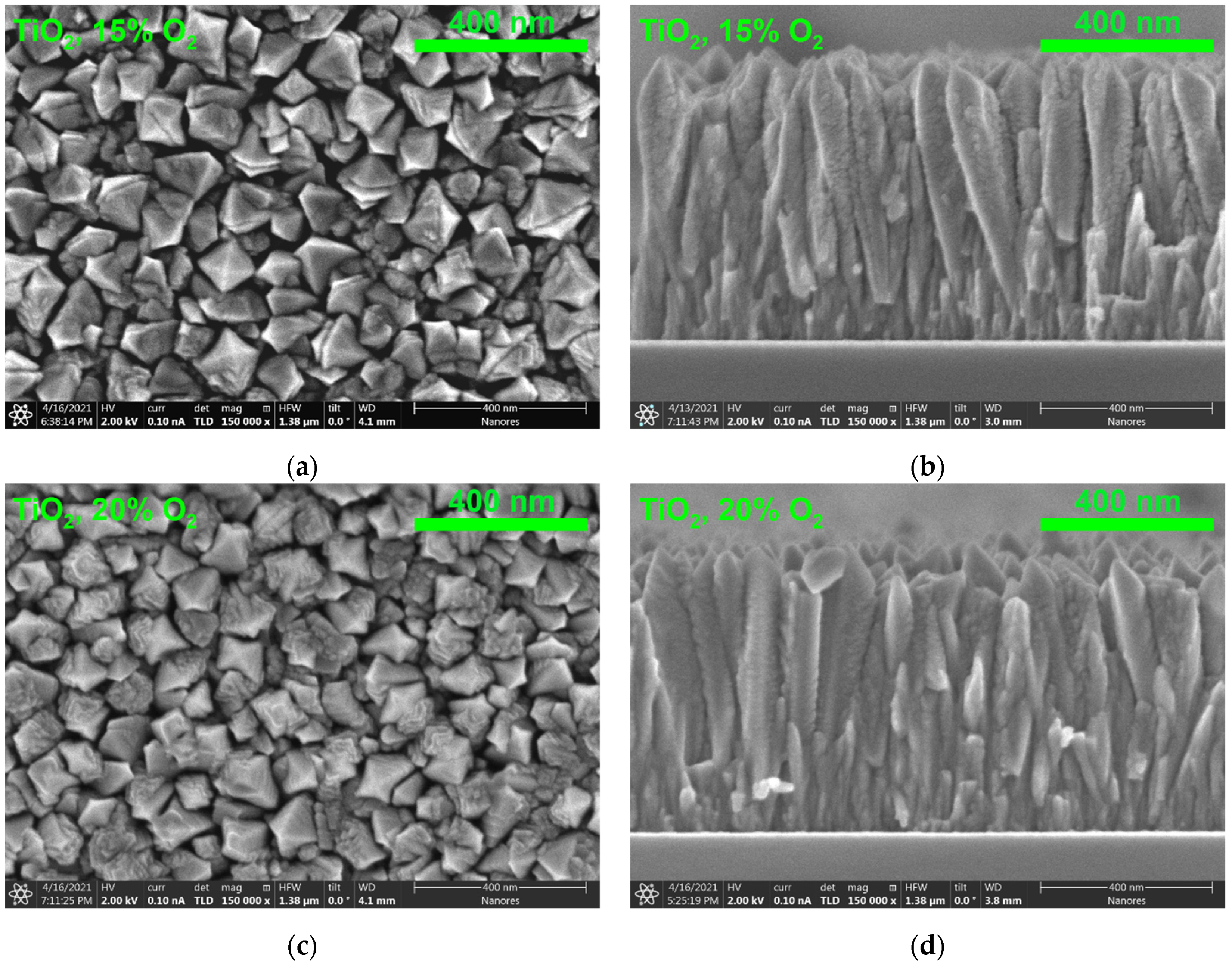
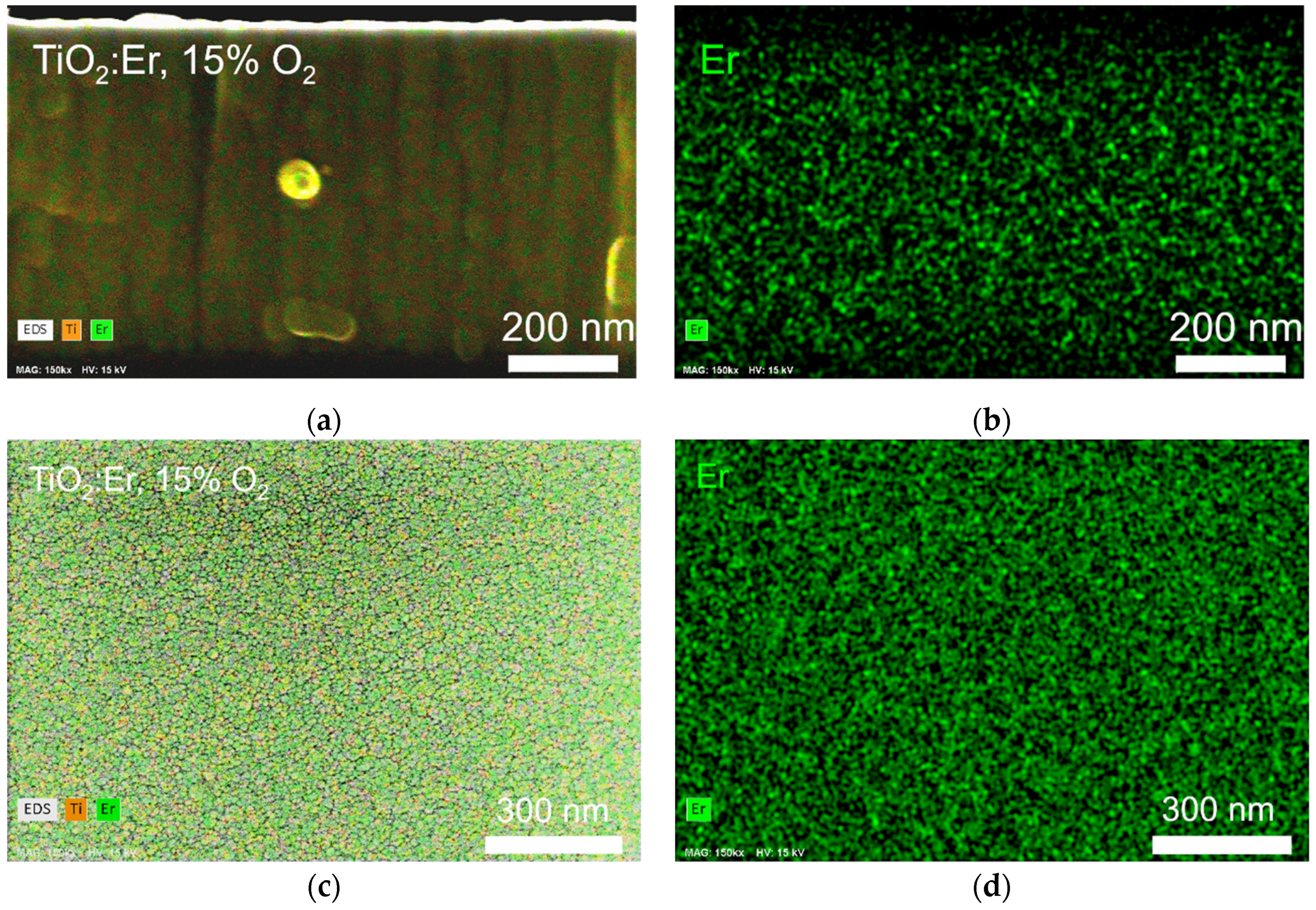
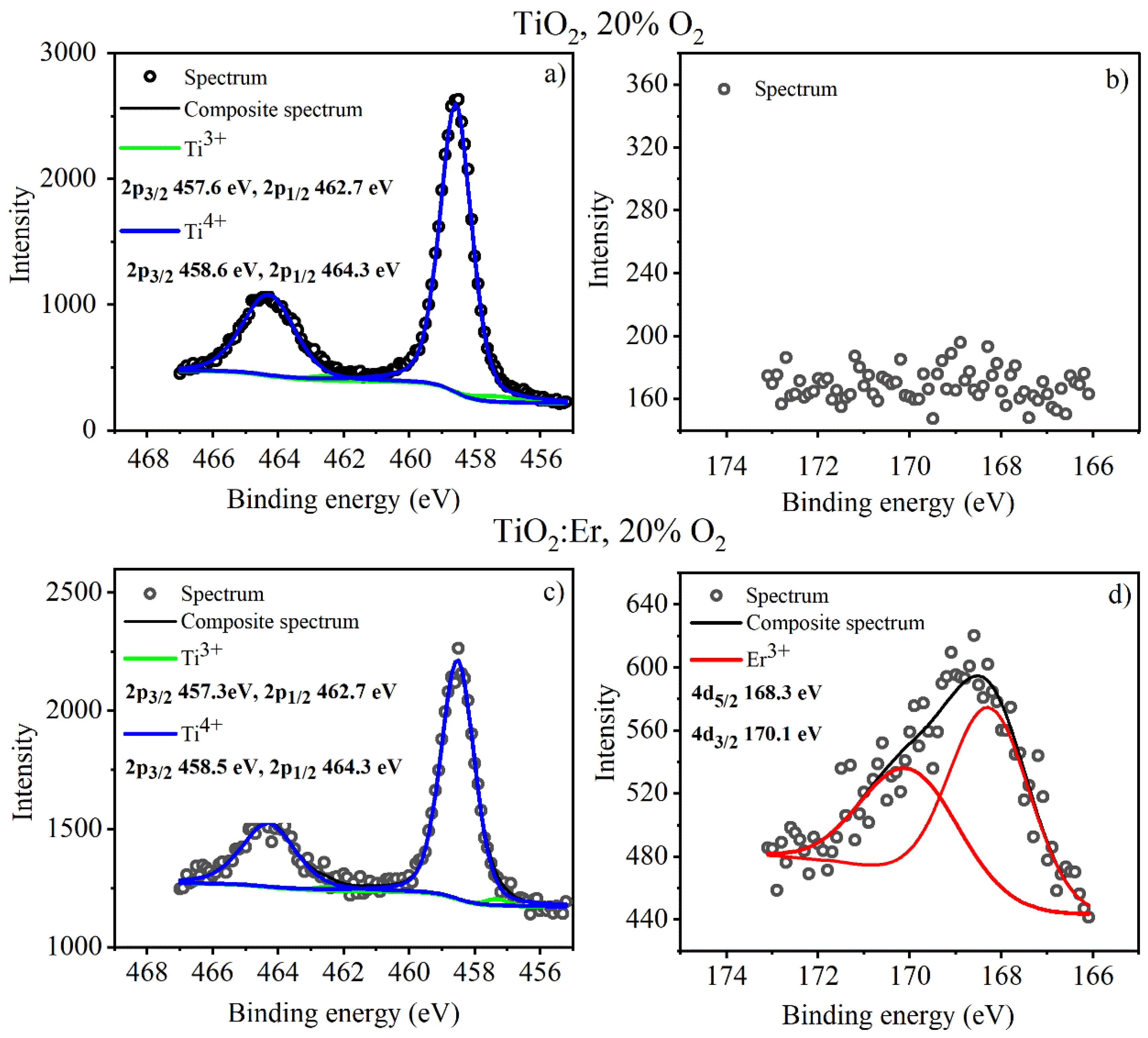
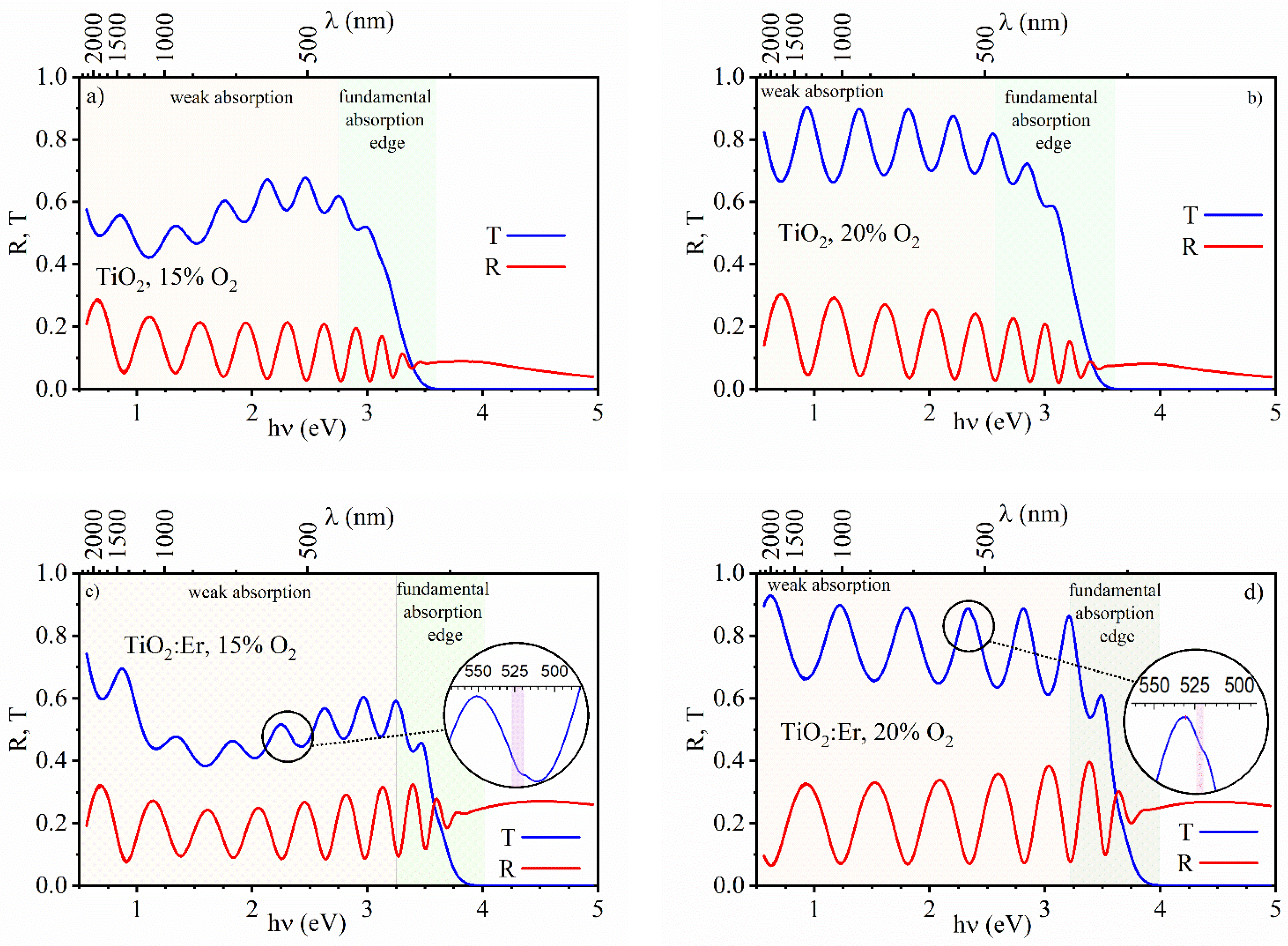
3. Results and Discussion

The XRD patterns recorded for thin films are presented in Figure 1. Undoped titanium dioxide thin films under these slightly nonstoichiometric conditions (15% and 20% O2) crystalized mostly as rutile (Figure 1a). However, at higher content of oxygen in the Ar + O2 mixture (20% O2), the onset of anatase precipitation was detected. At 2θ = 25.3° XRD line, which corresponds to the (101) plane of anatase (the reflex with the highest intensity) can be seen. For rutile, some differences in levels of signal intensities between TiO2 15 and 20% O2, and relative intensities from the 01-078-2486 card, were observed (Figure 1a). Thin films grow with crystallites not randomly oriented like grains in powder samples. Preferred orientation usually occurs. In the XRD setup, some crystallographic planes might be preferentially exposed to the incoming beam, and thus the intensity of the signal is higher.
In contrast to undoped TiO2, X-ray diffraction patterns of TiO2:Er thin films are featureless, indicating probable amorphization (Figure 1b). This effect was reported [33] and attributed to a significantly larger ionic radius of Er3+ ions (0.0890–0.1214 nm) than that of Ti4+ (0.042–0.074 nm). At a high concentration of Er3+, formation of erbium titanate pyrochlore structure, Er2Ti2O7 was observed [21] for samples annealed at a high temperature exceeding 800 °C. Significant increase in the X-ray intensity for 2θ between 28° and 38° occurs as seen in Figure 1b. To investigate the nature of this effect, the XRD patterns of amorphous silica substrate were collected. Then, the substrate pattern was multiplied by an empirical factor and subtracted from the pattern recorded for films. As a result, a broad peak with a maximum located at 21.5° (related to the amorphous substrate) was eliminated. This operation has put in evidence a wide feature, the maximum of which is located at around 30.5°. It is worth noticing that the reflex of the highest intensity from (222) planes of cubic Er2Ti2O7 occurs at 2θ = 30.7°. It may suggest the beginning of crystallization of nanosized Er2Ti2O7 or at least the presence of short-range order. Exemplary results before and after correction are presented in the Supplementary Materials, Figure S1.
The SEM images (Figure 2 and Figure 3) show that the substrates were homogeneously covered with thin films. An analysis of the surface and cross-sectional morphology of thin films confirms the conclusions drawn from the XRD studies. Well-crystalized pure TiO2 layers grow as well-shaped tetragonal columns with approximately 660 nm height (Figure 2b,d). The TiO2 layer’s surface is rough due to the pyramid-like tops of columns (Figure 2a,c). TiO2 columns have a tendency to enlarge their diameter with height and then to narrow due to the formation of the pyramid-like top.
In the case of TiO2 thin films containing Er, a smooth surface and compact growth of narrow fibers were obtained (Figure 3). A small change in the surface morphology is observed with the oxygen concentration during deposition; a higher amount of oxygen (20% O2; Figure 3c) leads to larger grains at the surface in comparison to grains at the surface of 15% O2 layer (Figure 3a). Moreover, thin fibers shown in Figure 3b for 15% O2 changed to thicker columns (Figure 3d) for 20% O2.
The grain analysis based on SEM images presented in Figure 2 and Figure 3 was carried out. The details concerning the distribution of the grain size can be found in the Supplementary Materials (Table S1). The average grain size of undoped TiO2 thin films is about 90–95 nm and does not depend on the oxygen concentration during sputtering. The average grain size of TiO2:Er films deposited at 15% O2 is about 14 nm and increases slightly to 19 nm for 20% O2.
The elemental composition of thin films was studied by the Energy Dispersive Spectroscopy EDS. The EDS spectra for pure TiO2 and TiO2:Er are presented in Figure 4. The measurement confirmed that all layers are composed of titanium and oxygen (Figure 4a–d). Moreover, for TiO2:Er samples (Figure 4c,d), peaks from Er (1.4, 6.9 and 7.8 keV) appeared. In all EDS spectra, a high-intensity peak assigned to Si originated from the substrate because the beam penetration depth was bigger than that of the thin film thickness. Additionally, due to the small size of samples, the signals from elements in an aluminum sample holder, copper clips and brass screws were collected. Thus, weak signals at 0.9, 1.0 and 1.5 keV can be attributed to copper, zinc and aluminum, respectively.
EDS elemental mapping for TiO2:Er deposited at 15% of O2 (Figure 5) demonstrates the homogenous distribution of erbium in the bulk (cross-section image; Figure 5a,b) and on the surface (Figure 5c,d) of thin films.
The XPS spectra of pure and Er-doped TiO2, deposited at 20% O2, are shown in Figure 6 within a region of binding energies covering Ti 2p (Figure 6a,c) and Er 4d peaks (Figure 6b,d). The Ti 2p spectrum was fitted with two 2p doublet structures (p3/2–p1/2 doublet separation equals 5.2 eV for Ti3+ state and 5.7 eV for the Ti4+ state) originating from two different states of Ti, which indicates the presence of nonstoichiometric titanium dioxide. Titanium is found mainly in Ti4+, which appears as a 2p3/2 line centered at 458.6 eV, but there is also a low concentration of Ti3+ oxidation state, which is expressed with 2p3/2 line at 457.3 eV [34].
The Er 4d spectrum was fitted with one doublet structure (d5/2–d3/2 doublet separation equals 2.05 eV) with main 4d5/2 centered at 168.3 eV, which indicates Er3+ oxidation state [35]. Table S2 in the Supplementary Materials contains the results of the XPS data fitting (peak position, its full width at half maximum FWHM and the area).
The composition of thin films was determined from XPS data presented in Table S2. The ratio of Er/(Er + Ti) derived from the analysis of the XPS peak area is about 0.14. As we demonstrated the uniform distribution of Er and Ti in the films (cross-sectional images presented in Figure 5a,b), it is reasonable to assume that this value represents not only the surface composition but that of the bulk as well.
The results of spectrophotometric measurements of the transmittance T and reflectance coefficient are presented in Figure 7. Regions of a weak absorption and fundamental absorption edge are marked. In the weak absorption region, the characteristic oscillations of T and R can be seen. They are related to the light interference at two interfaces: air–thin film and thin film–substrate. This behavior is very well known and described in many fundamental handbooks [36,37,38].
For a light incident on a film deposited onto a non-absorbing substrate, from the spectral dependence of the transmittance T and reflectance R coefficients over a weak absorption region, one can derive absorption coefficient and refractive index using a method described in detail in [39].
The transmittance coefficient of thin films deposited at 20% O2 is high and reaches 90% level for both TiO2 and TiO2:Er. Lower content of oxygen (15%) results in a decrease in T to approximately 65–60%. Furthermore, over the near-infrared range (at about 1000 nm), an additional extended minimum in T develops when thin films are deposited at 15% O2. The increased absorption within this spectral range could be explained by the departure from stoichiometry and increased concentration of defects such as oxygen vacancies [40,41].
The erbium-modified films (Figure 7c,d) exhibit additional absorption features marked with a circle and zoomed in. This additional absorption occurs at the wavelength of 525 nm, which corresponds to the strongest erbium absorption band. It might be evidence of erbium incorporation into TiO2 crystal lattice. Here, this effect is barely visible due to a relatively low amount of erbium in thin films with low thickness in comparison to powder samples (bulk material) with a similar concentration of erbium. This suggests that in the case of thin films, photoluminescence measurements are necessary to study the influence of lanthanides incorporated into TiO2. Within the region of the fundamental absorption edge, the transmittance coefficient abruptly drops to zero with the increasing photon energy hν. This effect is due to the band gap Eg of TiO2, which falls within the UV range of the light spectrum.
The absorption coefficient α was calculated independently in the weak and strong absorptions regions. Strong absorption appears close to the fundamental absorption edge. In the first step, the “envelope method” for transmittance and reflectance spectra was applied (exemplary results can be found in the Supplementary Materials, Figure S2. Then, the spectral dependence of the absorption coefficient within the weak and strong absorption region was determined (Figure 8). In Figure 8a,c, an increased light absorption over the VIS and NIR range for 15% O2 in comparison to 20% is shown.
The band gap energy Eg was determined from the cut-off of plots of (αhν)1/2 versus the photon energy hν at the zero-level, as shown in Figure 9. The band gap energy of undoped TiO2 is Eg = 3.04 eV for 15% O2 and 3.11 eV for 20%. The values for lower oxygen content correspond to the rutile band gap (3.0 eV), and for higher oxygen content, it is an effect of beginning the crystal phase transition from rutile to anatase (3.2 eV).
Such a shift of the band gap energy obtained from the analysis of the optical spectra is expected because the Eg of about 3.0 eV for rutile and of about 3.2 eV for anatase is usually reported [42]. Actually, the experimental uncertainty being of the order 0.01–0.02 eV is much smaller than the reported shift of 0.07 eV and can be explained by changes in the film crystallization, as suggested in Figure 1a.
However, in the case of TiO2:Er, the band gap energy Eg is certainly much bigger (3.42–3.45 eV) and does not depend so much on the oxygen content during the deposition of thin films. This significant blue shift in the fundamental absorption edge can be ascribed to the size-effect as a much smaller grain size was obtained for TiO2:Er. Nevertheless, the possibility of precipitation of nanosized crystals of the secondary phase Er2Ti2O7 cannot be excluded. The size of the nanocrystals being smaller than 5 nm remains in agreement with the extended uplift in the XRD intensity around 2θ = 30° (a broad feature appearing in Figure 1b and Figure S1).
There is not enough experimental evidence concerning the band gap of Er2Ti2O7. According to [43], the band gap of Er2Ti2O7 is about 3.39 eV, which coincides reasonably well with our observation. However, due to the lack of direct proof, the onset of Er2Ti2O7 precipitation remains a hypothesis in our work.
The luminescence properties of the active layers were measured in the UV-NIR range under the laser diodes at 980 nm and 488 nm wavelength excitation. In the first case (Figure 10a), a strong emission located around 1550 nm can be seen, which results from the typical 4I13/24I15/2 transition in erbium ions. The luminescence presented in Figure 10b reveals the up-conversion mechanism upon excitation at 980 nm. The emission peaks observed in the spectrum can be attributed to the following transitions in Er3+: 410 nm (2H9/24I15/2), 440 nm (4F3/24I15/2), 526–548 nm (2H11/2 (4S3/2) → 4I15/2) and 660 nm (4F9/24I15/2), as indicated in the scheme in Figure 10c. These emission peaks are possibly due to the three-photon excitation process described by 4I15/24I11/24F7/22G7/2. The excitation of the 2G7/2 level follows the non-radiative relaxation from the 4F7/2 level to the thermally coupled 2H11/2 and 4S3/2 levels. The absorption schemes were discussed in different low and high phonon environments as they determine luminescent transitions in RE ions [44]. The important aspect also concerns the cross-relaxation (CR) mechanisms in highly doped Er materials, which also can lead to the UP emission such excited state absorption (ESA) [45]. It might also promote other luminescent transitions, such as that at 615 nm (4G11/24I11/2) presented in Figure 10b, which was only registered in the fluoride low phonon materials (ZrF4-BaF2-LaF3-AlF3-NaF ZBLAN glass, NaYF4 crystals) [44]. The origin of the 490 nm band is related to the second harmonic of the 980 nm pump.
However, it is worth noting that the high concentration of Er ions induces the complex CR processes where energy transfer within the TiO2 band gap may not be excluded. When analyzing this aspect, the samples were excited at 488 nm, which led to the direct excitation of 4F7/2 erbium energy level and also corresponded to the sub-band excitation in TiO2. Under these conditions, the luminescence spectrum was registered within the wavelength range of 500–1100 nm, including undoped TiO2 samples for comparison (Figure 11a). When analyzing the erbium emission spectrum in both cases (15% and 20% O2), the characteristic intense transitions of 2H11/2 (4S3/2) → 4I15/2 and 4F9/24I15/2, assigned to the emission in the green (525 nm, 550 nm) and red (660 nm) part of the spectrum, were observed (Figure 11b). Moreover, in the NIR range, the luminescent bands at the wavelength of 800 nm (4I9/24I15/2), 850 nm (4S3/24I13/2) and much weaker at 980 nm (4I11/24I15/2) were recorded. By analyzing the spectra of undoped TiO2 thin films, the presence of bands in the range of 500–550 nm (2.48–2.25 eV, max. intensity 530 nm–2.5 eV), 580–725 nm (2.14 eV–1.7 eV), 840 nm (1.48 eV), 990 nm (1.25 eV) and 1050 nm (1.18 eV) was revealed. Green and red emissions are usually associated with the presence of oxygen vacancies and Ti3+ defects, respectively [46,47]. Oxygen vacancies can be located in a wide range of states (mid-gap), i.e., 2.269 eV (447 nm) to 2.719 eV (456 nm). However, in this case, radiation transitions from the TiO2 conduction band would have to take place, which is relatively unlikely, taking into account the 488 nm excitation. On the other hand, the visible luminescence (500–530 nm) may originate from the Ti3+ energy transfer to the surface oxygen vacancies [46,48]. The next two bands, i.e., at 840 nm and 990 nm, are related in particular to the emission in rutile TiO2 and the occurrence of self-interstitial defects of Ti4+ (Ti3+) [49].
Finally, the aspect of energy transfer between Er ions and the mid-gap levels of TiO2 should be mentioned here. Figure 11a shows a strong, wide red band from TiO2 overlapping with the emission of the 660 nm transition within the erbium energy bands. It may suggest the possible energy transfer from Er bands to TiO2 trap bands. Although it is not unequivocal at this stage, it proves the lack of clustering of erbium ions and the suitability of these layers in the up-conversion systems.

4. Conclusions and Perspectives

Optically active matrices such as fluorides and silicates doped with lanthanide ions are very well-known for efficient visible-to-UV [50] or NIR-to-UV [51] up-conversion. However, it was recognized that the incorporation of rare earth RE3+ ions into the TiO2 host becomes a big challenge because of the incompatibility of the ionic radii of RE3+ and Ti4+. Dordević et al., in review [23] on RE elements in anatase TiO2 nanoparticles, even used the term “unusual” with respect to the TiO2 matrix. Nevertheless, due to its excellent stability, TiO2 remains one of the most promising photocatalysts and candidates for photoanodes in water splitting. Many efforts focused on Er3+ ion incorporation in TiO2, as shown in an excellent review of Mazierski et al. [52]. Three other lanthanide ions, Ho3+, Tm3+ and Nd3+, incorporated in TiO2 anatase and their role in photocatalysis were discussed. It was pointed out that theoretical investigations by the density functional theory DFT method are quite scarce for these systems. Moreover, according to [52], there is no reliable proof that the up-conversion process has a real effect on improvement in photocatalytic activity.
In our work, comprehensive studies on TiO2 thin films with embedded Er3+ were undertaken. This system is known to demonstrate up-conversion from NIR (980 nm) to the visible range of the light spectrum (525–545 nm), and it is expected that by a three-photon nonlinear absorption, the UV range (390–410 nm) can be reached [53].
In conclusion, it was demonstrated that thin films of TiO2:Er deposited by magnetron sputtering:
  • Contain a high amount of Er (14 at.%);
  • Are amorphous to a large extent, but precipitation of the secondary phase of Er2TiO7 cannot be excluded;
  • Are smooth with the grain size much smaller than that of undoped TiO2;
  • Have the band gap energy much larger (0.4 eV blue shift) than that of undoped TiO2;
  • Exhibit up-conversion upon illumination at 980 nm;
  • Exhibit photoluminescence in the VIS and NIR range of the light spectrum upon excitation at 488 nm.
In the near future, it is intended to perform photoelectrochemical measurements with planar thin films photoanodes of TiO2:Er in order to assess whether there is a correlation between the efficiency of hydrogen generation and photoluminescent properties. The optimization of Er concentration will be accompanied by the incorporation of Yb playing the role of sensitizer.

Supplementary Materials

The following are available online at https://www.mdpi.com/article/10.3390/ma14154085/s1, Figure S1: XRD patterns (as measured and after correction) recorded for the Er-doped thin films deposited at 15% O2 (black curve) and 20% O2 (red curve). A correction was performed by subtraction of the recorded substrate pattern. Positions of reference peaks are marked with vertical lines. Reference patterns are from anatase 01-078-2486, rutile 01-086-0147, and Er2Ti2O7 01-073-1700 cards; Table S1: Grain size analysis; Table S2: XPS results analysis; Figure S2: Optical properties analysis of TiO2 thin films deposited at 20% O2—spectral dependence of: (a) the transmittance T and reflectance R coefficients with envelopes; (b) the calculated absorption coefficient α.

Author Contributions

Conceptualization, M.R. and K.Z.; methodology, M.R. and D.D.; validation, M.R., K.Z. and D.D.; investigation, A.K. and D.D.; writing—original draft preparation, A.K.; writing—review and editing, K.Z.; visualization, A.K.; supervision, M.R.; project administration, M.R.; funding acquisition, M.R. All authors have read and agreed to the published version of the manuscript.

Funding

National Science Center NCN project No. 2020/37/B/ST8/02539 is acknowledged.

Institutional Review Board Statement

Not applicable.

Informed Consent Statement

Not applicable.

Data Availability Statement

The data presented in this study are available on request from the corresponding author. The data are not publicly available due to the author’s readiness to provide it on request.

Acknowledgments

The authors want to thank Joanna Banaś-Gac for assistance during the deposition processes, Karol Kulinowski for providing the software for optical properties calculations, Adam Czapla for optical measurements, Edward Kusior for XRD measurements and Horiba Scientific for carrying out up-conversion and photoluminescence measurements.

Conflicts of Interest

The authors declare no conflict of interest.

References

  1. Zhang, F. Photon Upconversion Nanomaterials; Lockwood, D.J., Ed.; Nanostructure Science and Technology; Springer: Berlin/Heidelberg, Germany, 2015; ISBN 978-3-662-45596-8. [Google Scholar]
  2. Yang, R. (Ed.) Principles and Applications of Up-Converting Phosphor Technology; Springer: Singapore, 2019; ISBN 978-981-32-9278-9. [Google Scholar]
  3. Jayaraj, M.K. (Ed.) Nanostructured Metal Oxides and Devices; Materials Horizons: From Nature to Nanomaterials; Springer: Singapore, 2020; ISBN 978-981-15-3313-6. [Google Scholar]
  4. Gao, Y.; Shi, C.; Feng, J.; Zhao, G.; Yu, H.; Bi, Y.; Ding, F.; Sun, Y.; Xu, Z. Synergistic effect of upconversion and plasmons in NaYF4:Yb3+, Er3+, Tm3+@TiO2-Ag composites for MO photodegradation. RSC Adv. 2017, 7, 54555–54561. [Google Scholar] [CrossRef] [Green Version]
  5. Duan, C.; Liang, L.; Li, L.; Zhang, R.; Xu, Z.P. Recent progress in upconversion luminescence nanomaterials for biomedical applications. J. Mater. Chem. B 2018, 6, 192–209. [Google Scholar] [CrossRef]
  6. Dawson, P.; Romanowski, M. Designing ultraviolet upconversion for photochemistry. J. Lumin. 2020, 222, 117143. [Google Scholar] [CrossRef]
  7. Jarosz-Duda, A.; O’Callaghan, P.; Kuncewicz, J.; Łabuz, P.; Macyk, W. Enhanced UV Light Emission by Core-Shell Upconverting Particles Powering up TiO2 Photocatalysis in Near-Infrared Light. Catalysts 2020, 10, 232. [Google Scholar] [CrossRef] [Green Version]
  8. Yasaka, P.; Kaewkhao, J. Luminescence from lanthanides-doped glasses and applications: A review. In Proceedings of the 2015 4th International Conference on Instrumentation, Communications, Information Technology, and Biomedical Engineering (ICICI-BME), Bandung, Indonesia, 2–3 November 2015; pp. 4–15. [Google Scholar]
  9. Hu, S.; Qin, X.; Liu, X.; Zhou, G.; Lu, C.; Wang, S.; Xu, Z. Fabrication and luminescent properties of highly transparent Er3Al5O12 ceramics. Opt. Mater. 2017, 71, 86–89. [Google Scholar] [CrossRef]
  10. Wehrspohn, R.B.; Rau, U.; Gombert, A. (Eds.) Photon Management in Solar Cells; Wiley-VCH Verlag GmbH & Co. KGaA: Weinheim, Germany, 2015; ISBN 9783527665662. [Google Scholar]
  11. Tian, Q.; Yao, W.; Wu, W.; Jiang, C. NIR light-activated upconversion semiconductor photocatalysts. Nanoscale Horiz. 2019, 4, 10–25. [Google Scholar] [CrossRef]
  12. Johannsen, S.R.; Roesgaard, S.; Julsgaard, B.; Ferreira, R.A.S.; Chevallier, J.; Balling, P.; Ram, S.K.; Larsen, A.N. Influence of TiO2 host crystallinity on Er3+ light emission. Opt. Mater. Express 2016, 6, 1664–1678. [Google Scholar] [CrossRef] [Green Version]
  13. Khan, M.A.; Idriss, H. Advances in plasmon-enhanced upconversion luminescence phenomena and their possible effect on light harvesting for energy applications. Wiley Interdiscip. Rev. Energy Environ. 2017, 6, e254. [Google Scholar] [CrossRef]
  14. Wang, Y.; Zu, M.; Zhou, X.; Lin, H.; Peng, F.; Zhang, S. Designing efficient TiO2-based photoelectrocatalysis systems for chemical engineering and sensing. Chem. Eng. J. 2020, 381. [Google Scholar] [CrossRef]
  15. Eidsvåg, H.; Bentouba, S.; Vajeeston, P.; Yohi, S.; Velauthapillai, D. TiO2 as a Photocatalyst for Water Splitting—An Experimental and Theoretical Review. Molecules 2021, 26, 1687. [Google Scholar] [CrossRef]
  16. Fujishima, A.; Honda, K. Electrochemical Photolysis of Water at a Semiconductor Electrode. Nature 1972, 238, 37–38. [Google Scholar] [CrossRef] [PubMed]
  17. Radecka, M.; Kusior, A.; Trenczek-Zając, A.; Zakrzewska, K. Oxide Nanomaterials for Photoelectrochemical Hydrogen Energy Sources. In Advances in Inorganic Chemistry; Eldik, R., van Macyk, W., Eds.; Academic Press: Cambridge, MA, USA, 2018; Volume 72, pp. 145–183. ISBN 9780128150771. [Google Scholar]
  18. Stanley, C.; Mojiri, A.; Rosengarten, G. Spectral light management for solar energy conversion systems. Nanophotonics 2016, 5, 161–179. [Google Scholar] [CrossRef]
  19. Strümpel, C.; McCann, M.; Beaucarne, G.; Arkhipov, V.; Slaoui, A.; Švrček, V.; del Cañizo, C.; Tobias, I. Modifying the solar spectrum to enhance silicon solar cell efficiency—An overview of available materials. Sol. Energy Mater. Sol. Cells 2007, 91, 238–249. [Google Scholar] [CrossRef]
  20. Mao, X.; Yan, B.; Wang, J.; Shen, J. Up-conversion fluorescence characteristics and mechanism of Er3+-doped TiO2 thin films. Vacuum 2014, 102, 38–42. [Google Scholar] [CrossRef]
  21. Zhang, J.; Wang, X.; Zheng, W.-T.; Kong, X.-G.; Sun, Y.-J.; Wang, X. Structure and luminescence properties of TiO2:Er3+ nanocrystals annealed at different temperatures. Mater. Lett. 2007, 61, 1658–1661. [Google Scholar] [CrossRef]
  22. Salhi, R.; Deschanvres, J.-L. Efficient green and red up-conversion emissions in Er/Yb co-doped TiO2 nanopowders prepared by hydrothermal-assisted sol-gel process. J. Lumin. 2016, 176, 250–259. [Google Scholar] [CrossRef]
  23. Ðorđević, V.; Milićević, B.; Dramićanin, M.D. Rare earth-doped anatase TiO2 nanoparticles. In Titanium Dioxide; Janus, M., Ed.; IntechOpen: London, UK, 2017; ISBN 978-953-51-3414-5. [Google Scholar]
  24. Kiisk, V.; Akulitš, K.; Kodu, M.; Avarmaa, T.; Mändar, H.; Kozlova, J.; Eltermann, M.; Puust, L.; Jaaniso, R. Oxygen-Sensitive Photoluminescence of Rare Earth Ions in TiO2 Thin Films. J. Phys. Chem. C 2019, 123, 17908–17914. [Google Scholar] [CrossRef]
  25. Obregón, S.; Colón, G. Evidence of upconversion luminescence contribution to the improved photoactivity of erbium doped TiO2 systems. Chem. Commun. 2012, 48, 7865. [Google Scholar] [CrossRef] [Green Version]
  26. Kočí, K.; Reli, M.; Edelmannová, M.; Troppová, I.; Drobná, H.; Rokicińska, A.; Kuśtrowski, P.; Dvoranová, D.; Čapek, L. Photocatalytic hydrogen production from methanol over Nd/TiO2. J. Photochem. Photobiol. A Chem. 2018, 366, 55–64. [Google Scholar] [CrossRef]
  27. Mazierski, P.; Mikolajczyk, A.; Grzyb, T.; Caicedo, P.N.A.; Wei, Z.; Kowalska, E.; Pinto, H.P.; Zaleska-Medynska, A.; Nadolna, J. On the excitation mechanism of visible responsible Er-TiO2 system proved by experimental and theoretical investigations for boosting photocatalytic activity. Appl. Surf. Sci. 2020, 527, 146815. [Google Scholar] [CrossRef]
  28. Zakrzewska, K.; Kollbek, K.; Sikora, M.; Kapusta, C.; Szlachetko, J.; Sitarz, M.; Ziabka, M.; Radecka, M. Importance of the electronic structure of modified TiO2 in the photoelectrochemical processes of hydrogen generation. Int. J. Hydrogen Energy 2015, 40, 815–824. [Google Scholar] [CrossRef]
  29. Pérez, J.A.B.; Courel, M.; Valderrama, R.C.; Hernández, I.; Pal, M.; Delgado, F.P.; Mathews, N.R. Structural, optical, and photoluminescence properties of erbium doped TiO2 films. Vacuum 2019, 169, 108873. [Google Scholar] [CrossRef]
  30. Kot, A.; Dorosz, D.; Radecka, M.; Zakrzewska, K. Improved photon management in a photoelectrochemical cell with Nd-modified TiO2 thin film photoanode. Int. J. Hydrogen Energy 2021, 46, 12082–12094. [Google Scholar] [CrossRef]
  31. Gorni, G.; Velázquez, J.; Mosa, J.; Mather, G.; Serrano, A.; Vila, M.; Castro, G.; Bravo, D.; Balda, R.; Fernández, J.; et al. Transparent Sol-Gel Oxyfluoride Glass-Ceramics with High Crystalline Fraction and Study of RE Incorporation. Nanomaterials 2019, 9, 530. [Google Scholar] [CrossRef] [PubMed] [Green Version]
  32. Ishii, M.; Komuro, S.; Morikawa, T. Study on atomic coordination around Er doped into anatase– and rutile– TiO2: Er–O clustering dependent on the host crystal phase. J. Appl. Phys. 2003, 94, 3823–3827. [Google Scholar] [CrossRef]
  33. Yang, J.; Hu, Y.; Jin, C.; Zhuge, L.; Wu, X. Structural and optical properties of Er-doped TiO2 thin films prepared by dual-frequency magnetron co-sputtering. Thin Solid Films 2017, 637, 9–13. [Google Scholar] [CrossRef]
  34. Wagner, A.D.; Naumkin, A.V.; Kraut-Vass, A.; Allison, J.W.; Powell, C.J.; Rumble, J.R.J. NIST Standard Reference Database 20. Available online: http://srdata.nist.gov/xps/ (accessed on 8 April 2021).
  35. Uwamino, Y.; Ishizuka, T.; Yamatera, H. X-ray photoelectron spectroscopy of rare-earth compounds. J. Electron Spectros. Relat. Phenomena 1984, 34, 67–78. [Google Scholar] [CrossRef]
  36. Born, M.; Wolf, E. Principles of Optics; Electromagnetic Theory of Propagation, Interference, and Diffraction of Light, 5th ed.; Pergamon Press: Oxford, UK, 1975; ISBN 0-08-018018-3. [Google Scholar]
  37. Stenzel, O. Das Dünnschichtspektrum; Akademie Verlag: Berlin, Germany, 1996; ISBN 978-3527400966. [Google Scholar]
  38. Macleod, H.A. Thin-Film Optical Filters; Adam Hilder Ltd.: London, UK, 1969. [Google Scholar]
  39. Szczyrbowski, J.; Czapla, A. On the determination of optical constants of films. J. Phys. D Appl. Phys. 1979, 12, 1737–1751. [Google Scholar] [CrossRef]
  40. Grant, F.A. Properties of Rutile (Titanium Dioxide). Rev. Mod. Phys. 1959, 31, 646–674. [Google Scholar] [CrossRef]
  41. Breckenridge, R.G.; Hosler, W.R. Electrical Properties of Titanium Dioxide Semiconductors. Phys. Rev. 1953, 91, 793–802. [Google Scholar] [CrossRef]
  42. Landolt, H.; Börnstein, R. Numerical Data and Functional Relationships in Science and Technology, Volume 17 Semiconductors; Madelung, O., Ed.; Springer: Berlin/Heidelberg, Germany; New York, NY, USA; Tokyo, Japan, 1983. [Google Scholar]
  43. Sandeep, K. Ionic conduction properties of nanocrystalline Er2Ti2O7 functional material. Semicond. Phys. Quantum Electron. Optoelectron. 2020, 23, 52–59. [Google Scholar] [CrossRef]
  44. Aarts, L.; van der Ende, B.M.; Meijerink, A. Downconversion for solar cells in NaYF4:Er,Yb. J. Appl. Phys. 2009, 106, 023522. [Google Scholar] [CrossRef] [Green Version]
  45. Ivanova, S.; Pellé, F. Strong 1.53 μm to NIR-VIS-UV upconversion in Er-doped fluoride glass for high-efficiency solar cells. J. Opt. Soc. Am. B 2009, 26, 1930. [Google Scholar] [CrossRef]
  46. Abdullah, S.A.; Sahdan, M.Z.; Nafarizal, N.; Saim, H.; Bakri, A.S.; Cik Rohaida, C.H.; Adriyanto, F.; Sari, Y. Photoluminescence study of trap-state defect on TiO2 thin films at different substrate temperature via RF magnetron sputtering. J. Phys. Conf. Ser. 2018, 995, 012067. [Google Scholar] [CrossRef]
  47. Tariq, F.; Rehman, N.; Akhtar, N.; George, R.E.; Khan, Y.; Rahman, S. Room temperature photoluminescence in plasma treated rutile TiO2 (110) single crystals. Vacuum 2020, 171. [Google Scholar] [CrossRef]
  48. Choudhury, B.; Choudhury, A. Oxygen defect dependent variation of band gap, Urbach energy and luminescence property of anatase, anatase–rutile mixed phase and of rutile phases of TiO2 nanoparticles. Phys. E Low Dimens. Syst. Nanostruct. 2014, 56, 364–371. [Google Scholar] [CrossRef]
  49. Mi, Y.; Weng, Y. Band Alignment and Controllable Electron Migration between Rutile and Anatase TiO2. Sci. Rep. 2015, 5, 11482. [Google Scholar] [CrossRef] [Green Version]
  50. Zhang, W.; Yang, S.; Li, J.; Gao, W.; Deng, Y.; Dong, W.; Zhao, C.; Lu, G. Visible-to-ultraviolet Upconvertion: Energy transfer, material matrix, and synthesis strategies. Appl. Catal. B Environ. 2017, 206, 89–103. [Google Scholar] [CrossRef]
  51. Yu, Y.; Chen, G.; Zhou, Y.; Han, Z. Recent advances in rare-earth elements modification of inorganic semiconductor-based photocatalysts for efficient solar energy conversion: A review. J. Rare Earths 2015, 33, 453–462. [Google Scholar] [CrossRef]
  52. Mazierski, P.; Mikolajczyk, A.; Bajorowicz, B.; Malankowska, A.; Zaleska-Medynska, A.; Nadolna, J. The role of lanthanides in TiO2-based photocatalysis: A review. Appl. Catal. B Environ. 2018, 233, 301–317. [Google Scholar] [CrossRef]
  53. Obregón, S.; Kubacka, A.; Fernández-García, M.; Colón, G. High-performance Er3+-TiO2 system: Dual up-conversion and electronic role of the lanthanide. J. Catal. 2013, 299, 298–306. [Google Scholar] [CrossRef]
Figure 1. XRD patterns recorded for the thin films of: (a) pure TiO2 deposited at 15% O2 (black curve) and 20% O2 (red curve) and (b) Er-doped TiO2 deposited at 15% O2 (black curve) and 20% O2 (red curve). Positions of reference peaks are marked by vertical lines. Reference patterns are from anatase 01-078-2486, rutile 01-086-0147 and Er2Ti2O7 01-073-1700 cards.
Materials 14 04085 g001
Figure 2. SEM images of the surface and cross-section of undoped TiO2 thin films deposited at (a,b) 15% O2 and (c,d) 20% O2.
Materials 14 04085 g002
Figure 3. SEM images of the surface and cross-section of TiO2:Er thin films deposited at (a,b) 15% O2 and (c,d) 20% O2.
Materials 14 04085 g003
Figure 4. EDS analysis of TiO2 thin films: undoped TiO2 deposited at: (a) 15% O2 and (b) 20% O2; and TiO2:Er deposited at: (c) 15% O2 and (d) 20% O2.
Materials 14 04085 g004aMaterials 14 04085 g004b
Figure 5. EDS elemental mapping: (a,b) cross section and (c,d) surface of TiO2:Er deposited at 15% O2.
Materials 14 04085 g005
Figure 6. XPS spectra for the thin films of: (a,b) TiO2—deposited at 20% O2, and (c,d) TiO2:Er—deposited at 20% O2.
Materials 14 04085 g006
Figure 7. Spectral dependence of the transmittance T and reflectance R coefficients of thin films: undoped TiO2 (a) 15% O2 and (b) 20% O2; TiO2:Er (c) 15% O2 and (d) 20% O2. Additional absorption features zoomed-in circles.
Materials 14 04085 g007
Figure 8. Spectral dependence of the absorption coefficient α of thin films: undoped TiO2 (a) 15% O2 and (b) 20% O2, and TiO2:Er (c) 15% O2 and (d) 20% O2.
Materials 14 04085 g008
Figure 9. Band gap Eg determination for thin films—spectral dependence of the (αhν)1/2 coefficient vs. photon energy hν: undoped TiO2 (a) 15% O2 and (b) 20% O2; TiO2:Er (c) 15% O2 and (d) 20% O2.
Materials 14 04085 g009
Figure 10. Luminescent properties of Er-doped TiO2 thin films deposited at 15% O2 excited with 980 nm laser: (a) photoluminescence spectrum, (b) up-conversion spectrum, (c) energy diagram in Er3+.
Materials 14 04085 g010
Figure 11. (a) Luminescence spectrum of pure TiO2 and Er-doped TiO2 thin films deposited at 15 and 20% of O2 (enlargement in the inset) excited with 488 nm laser; (b) simplified diagram of possible transitions in Er3+.
Materials 14 04085 g011
Table 1. Parameters of thin films deposition process.
SampleTargetO2 Content in Ar + O2Thickness 1 (nm)Deposition Rate (nm/min)
TiO2, 15% O2Ti15%64012.8
TiO2, 20% O2Ti20%61012.2
TiO2:Er, 15% O2Ti/Er (90/10 at%)15%55011.0
TiO2:Er, 20% O2Ti/Er (90/10 at%)20%4809.6
Total flow rate 40 sccm; substrate temperature 350 °C; base pressure 10−7–10−8 mbar; sputtering pressure 6.3 × 10⁻³ mbar; sputtering power 200 W
1 Thickness measured by a stylus profilometer (Talystep, Taylor Hobson, Leicester, UK).
Publisher’s Note: MDPI stays neutral with regard to jurisdictional claims in published maps and institutional affiliations.

