Abstract
The main goal of this review is to comprehensively present the properties of silicon, germanium, and silicon-germanium systems and analyze current possibilities of producing fibers based on them for applications as a photovoltaic fabric for a future soldier. The vision of the future is to produce a feather-light photovoltaic optic fiber, exhibiting mechanical properties typical of Kevlar, enabling power/recharging of portable electric devices while simultaneously protecting against mechanical damage and explosions. This article analyzes, in detail, issues such as the occurrence and mobility of germanium in the environment, the life cycle of SiGe photovoltaic fabrics, ecotoxicological and human health implications, sustainable development strategies and policy implications, and analytical challenges due to low concentrations in the environment. Moreover, the advantages and disadvantages of silicon-based solar cells are analyzed, taking into account various factors, including environmental factors. Finally, the soldier of the future is analyzed.
1. Introduction
Semiconductors are the basis of (opto) electronic devices, including logic and memory devices, solar cells, displays, lasers, photodetectors, light-emitting diodes (LEDs), power devices, and quantum devices [1]. These semiconductors include both germanium and silicon. The properties of these semiconductors, such as energy gap (direct or indirect), bandgap energy, electron and hole mobility, dopability, thermal conductivity, chemical stability, and toxicity, determine their suitability for certain applications. Semiconductor materials vs. device applications are presented in Figure 1 and Table 1. Table 2 shows a comparison of the properties of these two semiconductors [2,3,4].
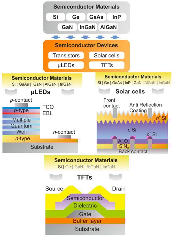
Figure 1.
Commonly used semiconductor materials and devices, prepared based on [4].

Table 1.
Semiconductor materials vs. device applications.
Table 2.
Physical properties of silicon and germanium at or near T = 27 °C, prepared based on [4].
In recent years, silicon and germanium-based materials have attracted considerable interest beyond conventional microelectronics, particularly in the form of semiconductor and multimaterial optical fibers [5,6,7]. In contrast to conventional silica optical fibers, semiconductor multimaterial optical fibers enable the simultaneous integration of optical, electrical, and thermal functionalities within a single, flexible structure, made possible by multimaterial thermal drawing and molten core fabrication techniques [6,7,8]. This unique capability has opened new opportunities for advanced sensing, imaging, and stimulation technologies, especially in biomedical applications, where minimally invasive and multifunctional probes are highly desirable [7,9].
Significant progress has been reported in the development of semiconductor multimaterial optical fibers for biomedical applications. Recent comprehensive reviews and experimental studies have demonstrated the use of semiconductor-integrated fibers as in-fiber photodetectors, temperature sensors, and chemical sensors capable of operating in biologically relevant environments [5,7,10].
Fibers incorporating silicon or germanium cores exhibit photoconductive and thermoresistive behavior, enabling distributed photodetection and localized temperature monitoring along the fiber length [6,8]. These functionalities are particularly relevant for biomedical applications such as pulse oximetry, fluorescence-based diagnostics, neural activity sensing, and monitoring of tissue heating during therapeutic and photothermal procedures [7,9].
Moreover, Ge-rich and SiGe alloy fibers extend optical operation into the near- and mid-infrared spectral regions, which are critically important for biomedical spectroscopy and imaging, including cancer diagnostics, blood analysis, and molecular fingerprinting of biological tissues [8,11]. The ability to engineer the composition, crystallinity, and geometry of Si–Ge fibers enables spectral tunability and enhanced sensitivity, offering clear advantages over traditional silica-based fiber platforms [6,11].
Beyond sensing and imaging, semiconductor multimaterial optical fibers have also been explored as flexible neural interfaces, where their mechanical compliance better matches that of soft biological tissues compared to rigid silicon probes [9,12]. By integrating optical waveguides with electrically functional semiconductor elements, these fiber-based systems allow for simultaneous optical stimulation and electrical recording, supporting advanced applications in optogenetics and neural monitoring [9,12]. Collectively, these developments highlight the growing relevance of SiGe-based fiber systems as multifunctional materials that combine low weight with advanced sensing and optoelectronic performance, making them attractive for both biomedical and defense-related applications.
1.1. Lightweight Materials for Defense Applications
The modern battlefield is characterized by the need for enhanced mobility, survivability, and operational efficiency. As defense platforms, including vehicles, aircraft, personal protective equipment, and structural components, evolve to meet increasingly complex mission requirements, the demand for advanced lightweight materials has increased substantially. These materials not only reduce the overall weight of defense systems but also contribute to improved fuel efficiency, increased payload capacity, faster deployment, and better performance. Importantly, lightweight materials must achieve this without compromising mechanical integrity, thermal stability, or resistance to hostile environments.
This paper presents the current research directions on lightweight materials in defense applications, focusing on metals, composites, ceramics, and novel multifunctional materials. Lightweight materials are central to the advancement of defense technology, enabling superior performance while maintaining the protection and durability required in harsh and unpredictable environments. Continuous innovation in material science, coupled with cross-disciplinary collaboration between chemists, engineers, and defense specialists, is essential to realize the full potential of these materials in next-generation defense systems. Lightweight materials can be a futuristic material that can develop the ability of defense equipment to enhance its strength, resistance towards high temperature, abrasion, wear and tear, and exposure to adverse environmental conditions (see Table 3) [13,14,15,16,17,18,19,20,21,22].
Table 3.
Examples of lightweight materials for defense applications.
1.2. Challenges and Future Directions
Despite the promising properties of lightweight materials, several challenges remain, such as the following:
- Cost-effectiveness: Many advanced materials, such as titanium alloys and carbon fiber-reinforced polymers (CFRPs), are expensive and resource-intensive to produce.
- Manufacturability: Processing techniques, joining methods, and repair strategies must be optimized for complex military systems.
- Durability and survivability: Materials must withstand extreme environmental conditions, long service lives, and hostile actions (e.g., ballistic impacts, high temperatures, corrosion).
- Life-cycle sustainability: Consideration of recyclability and environmental impact is becoming increasingly important in material selection.
Future research will likely focus on hybrid materials, integrated design approaches (e.g., topology optimization), and the use of artificial intelligence and machine learning to accelerate material production and performance prediction. The evolution of modern warfare and defense technology is driving the need for materials that are not only lightweight but also multifunctional, resilient, and adaptable. Future developments in lightweight materials for defense applications will be shaped by advances in nanotechnology, artificial intelligence, additive manufacturing, and sustainability. These trends aim to overcome current limitations and unlock new capabilities in performance, cost-efficiency, and mission adaptability.
A key future direction involves designing materials that perform multiple roles simultaneously, while reducing the complexity and weight of the system. Multifunctional materials can provide mechanical strength along with additional properties such as energy storage, sensing, thermal management, or camouflage (see Table 4). Nanotechnology is revolutionizing the design of lightweight materials by enabling precise control over structure and properties at the atomic or molecular level (Table 4). Additive manufacturing (AM) or 3D printing transforms the fabrication of complex lightweight structures optimized for strength and material efficiency (Table 4). Since traditional ceramics are brittle, future research should focus on making them more resilient and integrable with other materials (Table 4). Materials that can sense damage, respond to stimuli, or repair themselves will reduce maintenance needs and improve battlefield durability. Environmental and logistical concerns push the defense sector toward more sustainable material choices (Table 4). Moreover, artificial intelligence and machine learning are accelerating the pace of material innovation (Table 4) [23,24,25,26,27].
Table 4.
Challenges and future directions of lightweight materials.
The main goal of this paper is to comprehensively present the properties of silicon and germanium and to analyze the current possibilities of producing fibers based on them for applications as photovoltaic fabric for a future soldier.
The vision for the future involves the development of a lightweight photovoltaic optical fiber that exhibits high mechanical strength comparable to carbon fibers, excellent ballistic resistance similar to Kevlar, and conductive properties characteristic of optical fibers. Such a material would enable the powering and charging of portable electronic devices while simultaneously providing protection against mechanical damage.
Special attention was paid to the SiGe solidification process in terms of phase diagrams and analogy to water solidification, denoting that directional SiGe solidification in a strong thermal gradient could lead to a morphology characteristic of Janus dendrimers of diverse composition, useful in high-frequency microelectronic and nanorobotic applications.
Technical barriers to scaling up SiGe directional solidification for uniform long fibers: the realization of long, compositionally uniform silicon-germanium (SiGe) fibers via directional solidification remains a substantial materials and process engineering challenge. While recent work has demonstrated the potential for recrystallizing SiGe cores within glass-clad fibers to achieve single crystals and enhanced optical transmission, significant barriers hinder scalability for commercial photonic and photovoltaic applications [28,29,30,31], as is summarized in Table 5.
Table 5.
Summary of significant barriers that hinder scalability for commercial photonic and photovoltaic applications of SiGe.
In summary, the primary non-economic barriers to scaling SiGe directional solidification for long, uniform fibers include the following:
- ➢
- Compositional segregation and constitutional undercooling;
- ➢
- Thermal gradient and interface stability control;
- ➢
- Dopant diffusion and profile maintenance;
- ➢
- Structural defect suppression;
- ➢
- Crystal quality control through recrystallization;
- ➢
- Intrinsic phase behavior of SiGe alloys.
Addressing these challenges will require coordinated advances in thermal field management, real-time process monitoring, and innovative growth and post-processing technologies.
2. Results and Discussion
2.1. Selected Properties and Applications of Germanium
Germanium (Ge) is a hard, brittle element with a grayish-white, metallic luster. Its electrical behavior lies between that of a metal and an insulator. Depending on its end use, germanium is utilized either in its elemental form or as part of various compounds. Owing to its distinctive physical and chemical characteristics, it plays a vital role in many commercial, industrial, and military technologies. Key properties include the following:
- ➢
- It is an intrinsic semiconductor that can conduct electricity in its pure form, with particularly strong performance at high frequencies and low operating voltages;
- ➢
- It is transparent to certain wavelengths in the infrared spectrum;
- ➢
- It possesses a very high refractive index;
- ➢
- Similar to silicon, germanium is a glass-forming material, capable of creating extended three-dimensional networks composed of irregularly arranged germanium–oxygen tetrahedra;
- ➢
- It shows low chromatic dispersion.
These five properties define the usefulness of germanium in applications such as electronic components, night-vision equipment, fiber-optic cables, optical lens systems, and solar power technologies. In addition, germanium has a sixth important attribute: it can act as a catalyst in the polymerization of polyethylene terephthalate (PET) resin. This process is widely used in the production of polyester fibers and transparent plastic bottles, and germanium is particularly advantageous because it does not cause unwanted discoloration of the final plastic product, which is critical for certain uses [32]. In Japan, germanium dioxide is commonly employed as a catalyst in PET manufacturing. However, rising germanium prices have encouraged a shift toward alternative catalysts, such as antimony- or titanium-based compounds.
Between 2010 and 2016, global germanium consumption was dominated by infrared systems, which accounted for about 30% of total use. Fiber-optic applications and polymer catalysts each represented roughly 20%, while electronics and solar panels together made up approximately 15%. The remaining 15% was distributed among various smaller uses, including scientific research [33]. Other estimates of worldwide germanium utilization in 2016 show a similar pattern, with polymer catalysts accounting for 31%, fiber optics 24%, infrared optics 23%, solar cells 12%, and miscellaneous applications comprising the remaining 10% [34].
In the United States, the domestic end-use distribution was different and was the following: infrared optics (50%), fiber-optic systems (30%), electronics and solar electric applications (15%), and other uses, including chemotherapy, metallurgy, and phosphors (5%) [35,36]. In the United States, germanium is not utilized as a catalyst in polymerization processes [32].
Within the European Union, germanium consumption is mainly allocated to infrared optics (47%), fiber-optic applications (40%), and satellite solar cells (13%). It should also be emphasized that, in the EU, germanium is not used as a catalyst for PET polymerization, nor is it employed in the electronics industry [37].
Germanium is a key enabling element in silicon-based photonic materials, particularly in SiGe systems used for optoelectronic and photovoltaic applications. The review by Rosenberg [38] provides a comprehensive analysis of germanium occurrence, chemical speciation, and environmental stability, offering valuable foundational insight relevant to advanced photonic engineering. The strong chemical affinity between silicon and germanium facilitates controlled SiGe solidification, enabling precise tuning of refractive index, bandgap energy, and near-infrared (NIR) optical absorption. These properties are of particular importance for the development of flexible photovoltaic fibers, which operate efficiently in standard photonic and telecommunication windows (1.3–1.55 μm). From a defense photonics perspective, germanium-related material stability and oxidation behavior are critical factors influencing long-term performance under harsh environmental conditions. Although Rosenberg’s work focuses on environmental chemistry rather than device fabrication, the presented chemical framework directly supports material selection, processing strategies, and reliability assessment of SiGe-based fiber-integrated photovoltaic systems. Such technologies hold significant potential for next-generation military and dual-use photonic applications requiring mechanical flexibility, spectral tunability, and environmental robustness.
Germanium is used as a semiconductor material for optoelectronic and electronic applications. For example, high-brightness light-emitting diodes (LEDs) for backlighting liquid crystal display televisions and in vehicle headlights and taillights [39]. A less-expensive substitute for germanium in some electronic applications such as transistors can be silicon. However, there has recently been a shift back to the use of germanium, which is due to the fact that Ge semiconductors can be operated at higher processor speeds than Si chips [40].
Germanium wafers serve as the foundational substrate in multijunction solar cells. These photovoltaic devices achieve the highest efficiencies of any existing PV technology and are therefore used primarily in space and satellite applications [41].
The advantages of germanium-based cells include the following [32]:
- ➢
- Higher efficiency than silicon-based solar cells (over 25% compared to silicon-based solar cells), so fewer cells are required in a panel to produce equivalent amounts of power;
- ➢
- Smaller size;
- ➢
- High strength with minimal size;
- ➢
- Lower weight.
However, due to production costs, germanium-based cells are not widely used in terrestrial applications. Nevertheless, they have the potential to become economically competitive in the terrestrial solar cell market, as they are superior to typical silicon-based solar cells. Advances in production technology and increased production scale could reduce the cost of multijunction photovoltaic cells.
Moreover, germanium, a key element in the high-tech and defense sectors, is increasingly gaining attention due to its applications in silicon-germanium (SiGe) photovoltaic fibers. These fibers form the foundation of next-generation flexible photovoltaic fabrics—materials of strategic importance in modern military logistics and wearable electronics. However, while germanium’s role in enhancing photovoltaic performance is well established, its environmental behavior remains poorly understood. Modern military operations increasingly depend on energy autonomy, mobility, and rapid deployability. Lightweight, flexible photovoltaic (PV) materials embedded in uniforms, tents, or gear offer a transformative solution. Silicon-germanium alloy fibers, due to their enhanced optoelectronic performance, have emerged as key candidates for such applications. However, as the use of germanium grows, so does the need to understand its environmental implications, especially as it enters the biosphere through mining, manufacturing, and disposal processes. SiGe photovoltaic fibers combine the flexibility of textile materials with the high performance of thin-film photovoltaics. Their advantages include the following: high energy efficiency due to tunable bandgaps, mechanical flexibility, enabling integration into fabric, thermal stability for harsh environments, low weight-to-power ratio, critical for portable military systems. Applications include soldier uniforms with integrated power sources, mobile command tenting, surveillance drones, and sensor systems requiring on-the-go power generation.
Additionally, germanium is a trace metalloid with an average crustal abundance of 1.5–7 ppm. It primarily occurs as a substitute for silicon in silicate minerals and is commonly associated with sphalerite (ZnS), lignite, and fly ash from coal combustion. Ge mobilizes through weathering and is transported predominantly as Ge(OH)4 in aquatic systems, mimicking silicon behavior but with significant differences under specific pH and redox conditions. Adsorption onto iron and manganese oxides, as well as complexation with dissolved organic matter, plays a key role in its partitioning between solid and aqueous phases. Coal combustion, zinc ore smelting, and increasingly, the electronics and photovoltaics industry contribute to environmental Ge emissions. E-waste and processing residues are emerging as significant sources of localized contamination, raising concerns about leaching into soils and aquatic systems.
2.2. Production of Germanium
Germanium, a dispersed element estimated at 6.7 ppm in the Earth’s crust, is not found as a native metal but rather in trace amounts within common metallic ore minerals. Its industrial production primarily stems from two main sources: zinc ore processing and coal fly ashes, with the majority (around 60%) being a byproduct of zinc refining, and the remainder largely originating from fly-ash processing. Coal’s contribution to the global germanium supply is estimated to be between 20% and 30%. China is the leading global supplier of germanium, although a Canadian company is the largest single producer, contributing approximately 25% of the worldwide market supply from its British Columbia-based smelter and refinery. Belgium, Russia, and the United States are also significant contributors to the world’s germanium supply. The global supply of germanium is approximately 100 tons per year. While germanium’s primary production has shown a constant increase, reaching 160 tons in 2015, recycling efforts, particularly from post-consumer scrap, do not significantly contribute to the overall world supply due to the complexity and costs involved. However, internal scrap recycling can contribute over 50% of secondary sources [42].
The production of ultra-pure germanium from its concentrate involves a series of refining and purification steps. The cycle typically begins with the production of germanium concentrate, either as sulfide or oxide, followed by chlorination and subsequent distillation/purification to yield ultra-pure germanium tetrachloride (GeCl4). This is then converted to germanium dioxide (GeO2) and subsequently reduced to its metallic form. Further purification steps are undertaken depending on the required purity for the end application [42].
The germanium concentrate, typically ranging from 0.5 to 6% Ge, can be processed via either hydrometallurgical or pyrometallurgical routes. The hydrometallurgical route involves sulfuric acid leaching and subsequent oxidation of precipitates into GeO2. The pyrometallurgical method, commonly involving roasting or fuming, volatilizes GeO2, which is then collected from the fumes, achieving a tenfold increase in germanium concentration. Recycling of germanium scrap follows a similar path, forming Ge-dioxide for subsequent processing [42].
A crucial step in purification is the chlorination of concentrated germanium dioxide with hydrochloric acid, producing crude GeCl4 with minimal impurities, also in chloride form. Due to its higher boiling point, GeCl4 can be purified up to 6N through distillation, as impurities volatilize, making it suitable for industries such as fiber optics. For further purification, ultra-pure GeCl4 is hydrolyzed with deionized water to yield pure germanium dioxide, which is then reduced in a hydrogen atmosphere to its metallic form [42].
The production of high-purity germanium, particularly in single-crystal form, is crucial for advanced technological applications such as semiconductors. Post-processing techniques for recrystallization and purification are vital for improving the performance of germanium materials, especially in fiber formats.
Several bulk growth techniques are relevant to semiconductor core fiber fabrication, including germanium:
- Czochralski (CZ) growth: this is a common method for producing silicon crystals, where a crystal seed is slowly withdrawn from a molten material in a crucible, allowing atoms to attach to the seed. While primarily for silicon, the principles regarding thermal gradients and impurity incorporation are applicable.
- Bridgman–Stockbarger (vertical and horizontal) and float zone (FZ) growth are other directional resolidification techniques used for compound semiconductor materials and are relevant to understanding molten core drawing and post-processing of semiconductor core fibers [8].
- The molten core draw method (MCD) is widely used to fabricate semiconductor core fibers, in which a fluid melt core is contained by a glass cladding and drawn to fiber dimensions. As-drawn fibers are often polycrystalline, and post-processing treatments, such as directional recrystallization, are crucial to improve performance by reducing defects and impurity segregation at grain boundaries. Techniques like laser-heated pedestal growth (LHPG) and the traveling solvent FZ method are also employed, offering controlled recrystallization through moving thermal gradients. These advanced methods aim to produce single-crystal cores with high aspect ratios and reduced energy consumption compared to traditional wafer production [8].
2.3. Life Cycle of SiGe Photovoltaic Fabrics and Environmental Exposure
Germanium is primarily a byproduct of zinc mining and coal burning. Its extraction involves energy-intensive chemical separation, often using chlorination or solvent extraction, leading to potential emissions of toxic or reactive compounds.
The production of SiGe PV fibers may involve the following: (i) chemical vapor deposition (CVD) of Ge onto flexible substrates; (ii) high-temperature alloying of Si and Ge, and (iii) etching and doping processes to tune electrical characteristics. Waste streams from these processes can contain Ge residues, acids, and solvents, posing risks to industrial workers and surrounding ecosystems.
Military deployment of these fabrics poses minimal immediate environmental risks due to robust encapsulation. However, under field conditions—abrasion, UV exposure, or mechanical wear—there may be a release of microfibers or degradation products over time.
Improper disposal or incineration of SiGe PV fabrics could release germanium into the air, water, or soil. Recycling rates for Ge are low (<10%), highlighting the need for closed-loop recovery strategies in defense logistics [43,44,45].
2.4. Ecotoxicological and Human Health Implications
Germanium is not currently considered to be toxic at environmental levels, but some organogermanium compounds have shown nephrotoxic effects in laboratory mammals. There is a lack of data on long-term chronic exposure data in aquatic and terrestrial ecosystems. Potential risks in military settings are as follows:
- ➢
- Soldier exposure: Low likelihood during wear/use, unless materials degrade.
- ➢
- Localized contamination: Possible during manufacturing, especially without closed-loop recycling.
- ➢
- Waste management: Improper storage of discarded textiles may lead to groundwater contamination.
Monitoring Ge in environmental matrices is technically difficult due to the following: (i) low background levels; (ii) matrix interference from silicon; and (iii) complex speciation (e.g., particulate-bound vs. dissolved). Advanced techniques, such as inductively coupled plasma–mass spectrometry (ICP-MS) with isotope dilution or pre-concentration protocols, are needed for accurate environmental assessments. Sustainability strategies and policy implications are as follows:
- Green extraction and sourcing: (i) Recovery of Ge from fly ash and e-waste; (ii) use of byproduct Ge from industrial waste streams.
- Recycling technologies: (i) Fabric disassembly and Ge fiber extraction; (ii) pyrolysis or chemical stripping to recover alloys.
- Regulatory outlook: Military procurement policies must incorporate life-cycle impact assessments. Environmental management plans should address the safe use and disposal of Ge-containing PV systems.
Germanium-based photovoltaic fibers offer strategic advantages in modern defense applications. Yet, the environmental behavior of Ge, particularly its mobilization from military textiles during production and end-of-life stages, presents under-researched risks. Addressing these gaps through green design, responsible sourcing, and improved recycling infrastructure will ensure the sustainability of this promising military technology.
Germanium is a technologically critical element (TCE) with a growing role in numerous high-tech applications, including fiber optics, infrared optics, and semiconductor devices. Despite its increasing industrial relevance, germanium’s environmental presence and behavior remain significantly underexplored. Recent reviews have illuminated a range of concerns and gaps that limit our comprehension of Ge’s ecological and geochemical roles. This essay synthesizes the current state of knowledge and identifies major areas where further research is needed to understand germanium’s environmental fate and potential risks.
2.5. Germanium Status and Analytical Challenges Due to Low Environmental Concentrations
Germanium is recognized as a TCE due to its vital role in advanced technologies. However, its global production remains low compared to other critical elements, which may inherently limit its widespread environmental dissemination. While the modest production volumes suggest a limited direct pollution risk, indirect environmental impacts—particularly through coal combustion and industrial processes—cannot be discounted. Unfortunately, a lack of up-to-date and geographically comprehensive data prevents a robust assessment of Ge’s environmental footprint, especially in regions with a heavy reliance on coal-fired power generation.
One of the fundamental barriers to studying germanium in the environment is its extremely low natural abundance. In water bodies, Ge typically occurs in the nanogram per liter (ng/L) range, and in soils, concentrations are usually measured in low parts per million (ppm). This rarity makes analytical detection and quantification technically demanding. Instruments such as inductively coupled plasma mass spectrometry (ICP-MS) offer high sensitivity but still require careful sample preparation and pre-concentration steps. Moreover, the detection of methylated Ge species—potentially important in mobility and bioavailability—is particularly challenging. These analytical difficulties have contributed to the overall scarcity of reliable data and complicate efforts to build a cohesive understanding of Ge’s environmental dynamics [44,45,46,47,48,49,50].
2.6. Environmental Flows, Biogeochemical Cycles, and Interactions with Natural Matrices
Due to both limited data and measurement challenges, it is currently not possible to map germanium flows between environmental compartments such as soil, water, sediments, and biota. The lack of a quantifiable mass balance prevents researchers from constructing a detailed picture of germanium’s biogeochemical cycle. This knowledge gap restricts our ability to assess the long-term ecological implications of Ge inputs from anthropogenic or natural sources and undermines environmental modeling efforts. As such, defining the movement of Ge through terrestrial and aquatic systems remains an urgent priority for environmental geochemistry.
Another critical gap lies in our understanding of how germanium interacts with natural organic matter (NOM) and iron oxyhydroxides—two key substances that influence the fate and transport of trace elements in the environment. The lack of quantitative data on sorption behavior, complexation kinetics, and competition with other metal ions hampers the ability to predict Ge mobility and persistence in soils and waters. Furthermore, the role of homologous compounds and geochemically similar elements (such as tin or lead) in influencing the behavior of germanium remains largely unexplored. This incomplete knowledge poses challenges for risk assessment, particularly in disturbed or contaminated environments such as mining sites, wetlands, and industrial effluents [50,51,52].
2.7. The Overemphasis on Ge/Si Ratios
A significant body of environmental research on germanium has focused on its geochemical similarity to silicon (Si), often relying on Ge/Si ratios in studies of the weathering processes and circulation of silicon. While this approach has provided insights into silicate mineral breakdown and aquatic nutrient dynamics, it has inadvertently limited direct investigation into the specific behavior of Ge. The overreliance on Ge as a proxy for Si means that much of what is understood about germanium’s mobility, speciation, and reactivity is inferred rather than empirically established. It remains important to acknowledge that Ge often follows the Si cycle in systems dominated by diatoms and that weathering processes tightly link the two elements. However, this should not eclipse the need for independent studies focused solely on Ge [43,53,54,55,56,57].
2.8. Selected Properties and Applications of Silicon
Crystalline silicon accounts for roughly 95% of the global solar cell market. Silicon dominates the photovoltaic sector because it is widely available, abundant, and relatively inexpensive. The deployment of photovoltaic (PV) systems has expanded rapidly and continues to grow at a strong pace. Between 2011 and 2021, cumulative PV installations increased at an average annual growth rate (CAGR) of about 30% [58]. By 2023, worldwide installed PV capacity reached approximately 1177 GW, including around 239 GW of newly added capacity that year [59]. Silicon-based solar cells are manufactured as either monocrystalline or multicrystalline, a distinction that significantly influences their efficiency and overall performance. The advantages and disadvantages of silicon solar cells are presented in Table 6 [60,61,62,63,64,65,66,67,68,69,70,71].
Table 6.
Advantages and disadvantages of silicon solar cells, prepared based on [60,61,62,63,64,65,66,67,68,69,70,71].
Analysis of SiGe tandem cell performance indicates ~21.6% to ~30.6% theoretical efficiency under standard AM1.5G solar irradiance with solar intensity ranging from 1 to 1000 suns [72].
In the context of fiber-based photovoltaic systems, additional optical and electrical losses arise from curvature effects, reduced absorption path lengths, non-ideal light coupling, and material inhomogeneities introduced during fiber drawing. Consequently, a realistic upper-bound efficiency for semiconductor photovoltaic fibers can be conservatively estimated at approximately 20% [6,73]. This yields a theoretical maximum electrical power density of roughly 200 W·m−2 under full solar illumination.
In practical textile implementations, however, only a fraction of the fabric surface can be actively covered by photovoltaic fibers due to weaving constraints, mechanical flexibility requirements, and the need for electrical interconnections. Assuming an effective photovoltaic fill factor of 10–20%, consistent with reported fiber-based energy-harvesting textiles, the usable power density is reduced to approximately 20–40 W·m−2 [10,74]. For typical lightweight technical textiles with areal densities in the range of 200–400 g·m−2, this corresponds to a specific power of approximately 0.05–0.2 W·g−1.
For context, commonly carried soldier electronics such as tactical radios require continuous operational power on the order of 6–12 W [75]. Using the above estimates for a photovoltaic textile under optimal illumination, an active photovoltaic area of ~0.2–0.4 m2 could generate an average of 5–10 W under ideal sunny conditions. While actual daily irradiance and angles will substantially affect delivered energy, this analysis suggests that the concept of fiber-based photovoltaic power generation is realistic as a supplemental energy source, particularly for low-to-moderate power demands such as sensors, communications relays, and wearable electronics.
Our analysis shows that, while photovoltaic textiles based on SiGe fibers are not expected to fully replace primary battery systems for high-power loads, they can provide meaningful supplemental energy and extend battery life in wearable systems under appropriate environmental conditions. Achieving the higher end of the estimated power output will benefit from continued improvements in fiber photovoltaic efficiency, light management strategies, and textile integration techniques.
A representative example of early clothing-integrated photovoltaics is a winter outdoor jacket developed by Maier Sports within the German SOLARTEX project. First presented at the International Trade Fair for Sports Equipment and Fashion in Munich in January 2006, the jacket incorporated nine amorphous silicon solar modules supplied by Akzo Nobel, delivering a maximum output power of approximately 2.5 W under full solar illumination. The system was designed to power a portable MP3 player and demonstrated practical usability, providing more than 40 h of music playback after only three hours of exposure to full sunlight. This prototype illustrates the feasibility of integrating photovoltaic functionality into wearable textiles and achieving watt-level power outputs suitable for low-power portable electronics [76].
2.9. Electronics Based on SiGe for Operation in Extreme Conditions
Silicon-germanium (SiGe) is a highly suitable material, in the form of heterojunction bipolar transistors (HBTs) and power diodes, for use as a component in electronic devices that operate reliably in harsh conditions, including both extreme temperatures and radiation. It makes them strong candidates for aerospace, space exploration, and high-performance computing applications. The technological advantage lies in the high-quality growth of SiGe layers, prepared through reduced-pressure chemical vapor deposition at high temperatures. This technology has been widely studied, resulting in the optimization of conditions.
SiGe electronics possess a unique ability to withstand both high temperatures and cryogenic environments, where many other semiconductor devices suffer performance degradation. The precise nano-engineered SiGe prototypes studied by NASA scientists demonstrated that power diodes and transistors retain functionality under thermal cycling between −195 °C and +85 °C after 12 cycles, exhibiting stable forward conduction performance. As for the HBT structures with 5A and 50 V parameters built into all SiGe devices (power converter), the cryogenic environment appears to be more resistant, even reaching an exposure temperature of −243.15 °C [77].
SiGe HBTs have been exposed to radiation, simulating resistance to space-like and nuclear environments. Their intrinsic material properties, derived from the preparation method and heterojunction design, reduce sensitivity to heavy ion radiation, proton irradiation, and high doses of ionizing radiation. Simulation studies highlight that SiGe devices based on heterojunctionless tunnel field effect transistors, where a SiGe gate is deposited over the silicon substrate, exhibit smaller threshold voltage shifts, reduced peak transient currents, and less charge collection compared to other tested III-V compound semiconductors such as InAs and GaAs, indicating superior robustness in radiation-prone settings. The difference in performance was attributed to lower values of the voltage threshold difference between the low and high dosage levels [78].
2.10. Phase Diagrams and Solidification of SiGe
As mentioned above, considering electric properties, both Si and Ge are monoatomic semiconductors (intrinsic semiconductors), and under normal pressure, they have a diamond-type structure and crystallize in a regular lattice with crystal lattice constants of 0.54307 and 0.56575 nm, respectively. The melting point of Si is 1414 °C, while Ge is equal to 938.25 °C [79]. Under normal pressure, the SiGe two-phase system forms a solution both in the liquid and solid state and crystallizes in the temperature range as presented in the phase diagram (Figure 2). The points corresponding to the temperatures of the beginning of crystallization form a line called the liquidus curve, while at the end of crystallization, there is a solidus curve. The area between the above curves is a two-phase region, the equilibrium coexistence of a liquid solution with a solid solution. So, the SiGe system creates two stable phases under normal pressure: liquid and the cubic diamond-type substitutional solid solution [80].
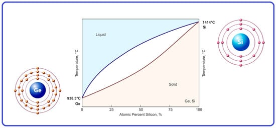
Figure 2.
The phase diagram of the SiGe system, prepared based on [80].
Under high pressure, both Si and Ge have a β-Sn type structure and crystallize in a body-centered tetragonal (bct) structure with crystal lattice constants of a = 0.4686, b = 0.2585 (Si) and a = 0.4884, b = 0.2692 (Ge) [80]. The SiGe system transforms under high pressure to a two-phase mixture at a low temperature range (below 300 K), and a bct structure of the SiGe solid solution is more stable at high pressures (above 300 kbar) than the diamond-type structure at lower pressures [81,82,83,84]. The behavior of pristine Si and Ge as well the SiGe system during the solidification process at various conditions has been previously studied by many groups [28,85,86,87]. It was shown that they all expand during solidification, and the permanent solidification should be associated with an increase in pressure. The SiGe system behaves similarly to water during solidification. Water is known to solidify dendritically, forming beautiful snowflakes. Similarly, quenched SiGe microdroplets enclosed within glass fibers exhibit a dendritic morphology [31]. In addition, Ge has been found to have a higher solubility in the liquid state (with a total solubility of Si and Ge in both solid and liquid states) and at sufficiently low solidification rates, the initial solid-phase nuclei are rich in Si, and as solidification progresses, more and more Ge is rejected into the alloy, and an inhomogeneous distribution of Ge occurs (slow diffusion of solute in the solid). Such directional solidification of SiGe in a strong temperature gradient leads to the formation of compositionally segregated particles, called Janus particles [88]. On the other hand, it is known that it is difficult to achieve stable solidification front propagation and Janus morphology because constitutional supercooling of the alloy occurs, which leads to the growth of dendritic or cellular morphology [85,86]. However, Gemennik et al. [31] used a flame breakup approach to produce compositionally segregated Janus particles of SiGe in a scalable manner. They showed that the in-fiber breakup method allows for the creation of SiGe microparticles with Janus morphology as well as Si microparticles with a high level of internal stress, thanks to limited solidification in the silica cladding. They also showed that by precisely controlling the cooling rate, it is possible to recrystallize particles post-breakup and to change the orientation of the Janus particle axes.
Summarizing, the directional SiGe system solidification in a strong thermal gradient could lead to a morphology characteristic of Janus particles of diverse composition, which may be relevant for applications, for example, in high-frequency microelectronics and nanorobotics. The high pressure generated during slow cooling can potentially change the band structure of these materials [89,90], which could find application in photovoltaics.
Moreover, it is well known that typically, inhomogeneity is a defect that harms efficiency by creating recombination centers. But on the other hand, as mentioned in [91], the Janus-like nanoparticles can find application in thin-film solar cells because they increase infrared absorption. Also, for the same reason, they could be used in infrared photodetectors and light-emitting diodes. However, it should be stressed that the precise control over the morphology, structure, and size of Janus particles is required for application because their properties depend on it. On the other hand, as reported in [89,90], the internal stresses could allow the bandgap of materials to be controlled, which could also find application in photovoltaics. Taking into account fibers, as shown in [31], it is possible to obtain SiGe Janus-type particles with a high level of internal stresses and their reorientation by laser recrystallization, which can lead to the construction of in-fiber arrays of SiGe Janus-type particles connected to metal buses, thus creating fully integrated microelectronics in the optical fiber. Finally, in Table 7, we show clarification of our intent and relevance to PV fibers in the Janus dendrimers morphologies.
Table 7.
Clarification of our intent and relevance to PV fibers in the Janus dendrimers’ morphologies.
Finally, while dendritic solidification can, in other material systems, be exploited to produce Janus morphologies for non-PV applications, in the present work, such compositional asymmetry is considered a defect; the SiGe phase diagram is used here specifically to define growth conditions that yield a homogeneous, high-quality photovoltaic absorber.
2.11. High-Performance Fibers
The advancement of military technologies necessitates the development and implementation of advanced materials, among which fibrous composite materials with tailored mechanical and thermal properties play a crucial role. Key performance parameters for such materials include Young’s modulus, tensile strength, elongation at break, chemical resistance, thermal degradation resistance, thermal capacity, and infrared emissivity. Although a broad body of literature addresses these materials, particular attention should be paid to the works presented in the references [92,93]. The publication [92] constitutes a comprehensive review of high-performance fibers, providing an in-depth discussion of the current state-of-the-art, chemical structures, mechanical properties, and future challenges associated with these materials. The authors offer a detailed classification of high-performance fibers, encompassing both organic types (e.g., Kevlar®, Nomex®, Vectran®, Zylon®, M5®, and ultra-high-molecular-weight polyethylene such as Dyneema® and Spectra®) and inorganic fibers (including carbon, glass, boron, and ceramic fibers). The chemical structures of some high-performance organic fibers are presented in Figure 3.
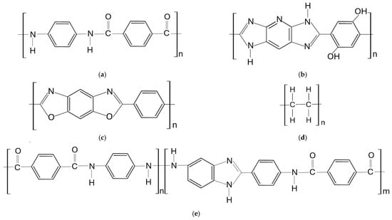
Figure 3.
Chemical structures of high-performance organic fibers: (a) Kevlar fiber, (b) M5 fiber, (c) PBO fiber, (d) UHMWPE, (e) Armos fiber.
Special emphasis is placed on the correlation between molecular structure and physico-mechanical performance characteristics, such as tensile strength, Young’s modulus, and resistance to ultraviolet radiation, thermal loads, and chemical agents (Table 8 and Figure 4).
Table 8.
Properties and applications of high-performance fibers, prepared based on [94].
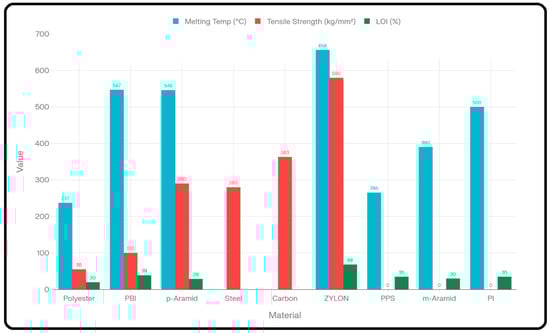
Figure 4.
Mechanical properties and flame resistance of Zylon® and other high-performance fibers, prepared based on [95].
Particular attention has been devoted to aramid fibers, such as Kevlar® and Nomex®, which exhibit exceptional mechanical performance due to their rigid polymer chains and strong intermolecular hydrogen bonding [96]. Modern fiber manufacturing techniques such as gel spinning, dry-jet wet spinning, die-drawing, and isothermal bath processing have also been discussed, as they enable the production of fibers with exceptional molecular orientation and high crystallinity. A particularly compelling issue is the observed discrepancy between the theoretical and experimentally measured mechanical properties, which highlights the considerable potential for further advancement of these materials in terms of both strength enhancement and optimization of production costs. Moreover, the susceptibility of certain high-performance polymers to ultraviolet (UV) degradation has been identified and remains a critical challenge in material design for extreme applications [97]. Typical mechanical properties of Kevlar fibers compared with PV fiber are shown in Table 9 [98].
Table 9.
Typical mechanical properties of Kevlar fibers compared with PV fiber.
Currently, many researchers are focusing on the development of fibers capable of harvesting solar energy. A T-shirt, winter coat, or other garment incorporating photovoltaic fibers could not only maintain thermal comfort for the human body but also supply electric energy to, for example, power a mobile phone, flashlight, or other personal electronic devices. To date, several application areas have successfully combined the concept of photovoltaic textiles with solar panels, including shading façades that simultaneously provide energy and awnings used for street lighting. Another emerging concept involves the production of solar-powered tents. This is particularly relevant for military tents used in locations (training grounds) situated at a considerable distance from accessible electrical power sources. An additional advantage of such tents would be the possibility of heating their interior during nighttime using stored energy, as well as eliminating the need for power generators that produce significant noise.
Materials with conductive functionality intended for such structures must also exhibit appropriate mechanical properties. The longitudinal elastic modulus of a standard Si0.5Ge0.5 optical fiber at room temperature is approximately 98 GPa [99], while its tensile strength is about 3 GPa. Therefore, the fabricated fibers should be characterized by mechanical parameters comparable to or superior to those of currently produced fibers.
Moreover, it should be stressed that recent semiconductor fiber research (e.g., Si and Ge fibers with optoelectronic function) shows mechanical properties that are orders of magnitude lower than Kevlar but still promising for integration into flexible fabrics. For example, the tensile strength for standalone Si fiber is ~338 ± 144 MPa, while for standalone Ge fiber, it is ~506 ± 105 MPa, which is much lower at this moment than for Kevlar. Additionally, the bending radius tolerance is functional after bending to ~2.5–5 mm radius, indicating good flexibility, while impact strength is ~4.7–4.9 MJ/m2 and torsional break stresses are ~245–273 MPa before failure [100].
In summary, the presented values indicate that current SiGe semiconductor fibers are mechanically robust enough for manual weaving and moderate bending and are far below conventional high-performance polymer fibers like Kevlar in tensile strength (Kevlar is several GPa versus hundreds of MPa for Si/Ge fibers) [98].
The main question is, why the gap? The answer is simple. Si and Ge materials are intrinsically brittle compared to polymers; even in nanowire or fiber form, they do not readily achieve Kevlar-level ductility or strength without advanced structural engineering [101]. Semiconductor fiber research is primarily focused on integrating optoelectronic functionality and manufacturability (long lengths and high quality), not yet on optimizing mechanical toughness or specific strength (Table 10).
Table 10.
Summary of reported Kevlar-like target fiber and current SiGe fibers’ properties.
The research presented in [93] focuses on the development of flexible, nanofibrous Kevlar aerogels (KNAs) and their composites with phase change materials (PCMs), specifically tailored for infrared stealth and thermal camouflage applications. The authors fabricated thin, lightweight, and highly porous Kevlar nanofiber-based aerogel films exhibiting excellent thermal insulation properties and a large specific surface area. Upon impregnation with polyethylene glycol (PEG) and coating with a fluorocarbon-based layer, these structures formed KNA/PCM composites characterized by a low emissivity in the 3–15 μm infrared spectrum and the capacity to absorb and store heat within the melting range of the PCM. Experimental results demonstrate that under dynamic solar irradiation conditions (e.g., day–night cycles), the application of KNA/PCM films onto objects allows for effective thermal camouflage, rendering the object thermally indistinguishable from the background in infrared imaging. Furthermore, multilayer hybrid structures (KNA−KNA/PCM) were proposed, combining insulating and energy-absorbing layers. These systems efficiently suppress both heat transfer and infrared radiation, thus enabling even hot targets to evade detection by dedicated detection systems [93]. Experimental results demonstrated that KNA films exhibit an exceptionally low thermal conductivity coefficient (0.036 W/m·K), high thermal stability (up to 400 °C), and mechanical strength comparable to or exceeding that of conventional aerogels.
In summary, the first paper [92] provides a comprehensive overview of various high-performance fibrous materials, addressing their molecular architecture, applications, and technological limitations. In contrast, the second one [93] introduces an innovative solution in the form of a lightweight and functional KNA/PCM composite designed for military and industrial stealth applications. Both articles converge on the theme of advanced materials with superior performance metrics tailored for operation in demanding environments. However, paper [93] also offers experimental validation of the composite’s effectiveness, highlighting its practical potential.
2.12. Semiconductor Core Fibers
Novel core fibers, particularly those with semiconductor cores, offer a wide range of applications in optics, serving as sources, detectors, and non-linear response media. The development of methods for drawing fibers with a semiconductor core has enabled optoelectronic and even electronic device applications. This field emphasizes glass-clad, crystalline core fibers, with research focusing on the underlying materials science, post-processing techniques for recrystallization and purification, and the influence of core material phase diagrams on performance and future prospects.
While traditional silica glass optical fibers are prevalent due to their transparency and design flexibility in communications, “multimaterial” or “hybrid” fibers that co-process disparate material families have emerged as a challenge for silica in specialized applications. These multimaterial fibers leverage a broader spectrum of the periodic table, offering a wider array of interesting and useful properties through diverse core and cladding materials. A significant area of development involves the pairing of a glass cladding with a crystalline semiconductor core, introducing electronic, thermoelectric, optoelectronic, optically non-linear, and mechanical properties not found in glasses [8].
The primary method for fabricating semiconductor core fibers is the molten core draw (MCD) method (historically known as the molten core method or MCM). In this technique, a fluid melt of the semiconductor core is contained by a glass cladding, and the combination is drawn into fiber dimensions. This method allows for scalable production, yielding hundreds of meters of fiber from single runs, and facilitates the rapid exploration of new material systems without requiring equipment modification. Both unary and complex semiconductors have been studied using MCD, with routine fabrication lengths exceeding hundreds of meters, typically limited by preform dimensions. A limitation of this technique is that the fiber cannot be drawn with a cladding glass that softens above the sublimation or boiling point of the core constituents. As-drawn MCD fibers are typically polycrystalline, which can lead to inferior performance for many applications due to crystalline disorder, impurity segregation at grain boundaries, optical and electronic defects, scattering and absorptive losses, mechanical weakness, and short electronic carrier lifetimes. The presence of grain boundaries can also result in compositional inhomogeneity, particularly in alloy systems, due to component segregation at the solidification boundary [8]. Other fabrication methods include the following:
- High-Pressure Chemical Vapor Deposition (HPCVD): Some of the earliest semiconductor core optical fibers were made using HPCVD inside a pre-drawn micron-sized pore of a glass capillary. This method offers high purity from gas precursor reactants and the ability to deposit materials that might vaporize in conventional MCD processes. It uses lower temperatures, resulting in amorphous or small-grain polycrystalline materials, and typically produces fibers tens of centimeters long with substantial growth times [8].
- Pressure-Assisted Melt Filling (PAMF): This technique involves forcing a molten core material into a smaller diameter pore of a spliced fiber. It has been frequently used for fabricating germanium core materials [8].
Post-processing treatments are crucial for promoting directional recrystallization of the core, significantly improving fiber performance. The fiber geometry allows for the imposition of unusually large spatial temperature gradients and high solidification velocities within a contamination-limiting containment vessel. The fabrication of single-crystal cores with aspect ratios exceeding 104 is becoming common [8].
Methods used for post-fabrication annealing and recrystallization of continuous crystalline core fibers include the following [8]: oven thermal annealing, rapid photothermal annealing, laser treatment (at both visible and IR wavelengths), and diverse heating methods in tapered rigs.
Laser-driven translation of a melt zone through the core has become a dominant technique due to its rapidity and ability to minimize core variations over millimeter length scales if the molten zone is long compared to the core diameter. Laser treatment can achieve the largest temperature gradients (exceeding 104 K cm−1). These rapid melt/recrystallization cycles with extreme temperature gradients can segregate impurities through thermomigration and liquid–solid segregation coefficients. For unary semiconductors, rapid melt zone translation minimizes additional nuclei growth, reducing polycrystallinity. For alloys, slower translation is preferable due to finite diffusion coefficients and constitutional undercooling. Multi-component systems can simplify single-crystal production, as the component with the lowest melting point can act as a moving solvent [8].
The selection of cladding glass, draw temperature, and post-processing conditions is contingent on the melting and/or vaporization temperature of the semiconductor core. For multi-component cores, understanding the equilibrium phase diagram, including two-phase fields, eutectic points, or additional phases, is essential. The rapid fiber draw process typically suppresses macroscopic phase segregation, but post-processing with thermal gradients can produce various compositional structures. Single-component cores and multi-component cores can be distinguished [8].
Single-component cores:
- Germanium (Ge): Germanium was among the earliest semiconductor core fiber materials explored using HPCVD. Its accessible melting point (~940 °C) has led to extensive study. Studies on crystallized Ge cores have shown potential for mid-IR devices. MCD draws of Ge core fibers have been made with both borosilicate and silica cladding glasses. Post-fabrication processing, including tapering, oven annealing, and laser annealing, has improved mechanical and optical properties.
- Silicon (Si): Silicon is the most studied core material due to its transparency at telecom wavelengths and expertise gained from planar silicon photonics. Most MCD fabrication uses bulk silica cladding. Post-processing significantly improves optical losses and grain size. Stress caused by silicon’s nearly 10% volume expansion upon solidification is a key consideration, limiting maximum core size.
- Selenium (Se) and Tellurium (Te): These elements also demonstrate phase behavior relevant to single-component cores. Phosphate glass-clad fibers with crystalline SeTe cores have been studied and used as stress sensors and photoconductors.
Multi-component cores:
- SiGe: Fibers are typically drawn at temperatures around 1950 °C, using silica as the cladding. Compositional variations are observed in as-drawn material due to preferential solidification of silicon from the melt, but laser annealing can create a more homogeneous structure. Germanium’s lower melting point allows it to act as a solvent, promoting large single-crystalline core regions.
- Si/GaSb: This pseudo-eutectic ternary system has been reported as a core material, where GaSb acts as a low-temperature solvent for silicon, leading to highly crystalline cores with classic eutectic features.
The fiber format offers several advantages: direct accessibility of the semiconductor phase to light, high surface quality of semiconductor-in-glass waveguides, internal microstructuring capabilities via thermal treatment, and a wide choice of core materials. Fibers also provide a route to single-crystal production with reduced energy consumption and conservation of less earth-abundant materials, as they typically utilize the entire precursor semiconductor charge. Additionally, fibers are beneficial for detector arrays, where the glass cladding can isolate individual elements, provide mechanical stability, and support deposited electrodes. The extreme aspect ratios achieved with fiber technology offer extraordinary thermal and mechanical properties for single crystals [8].
The predominant application of semiconductor core fibers to date has been in optics, including improved broadband transmission, photodetection, and light sources. As control over core composition and structure improves, new applications are emerging. Photonics, including linear and non-linear optical applications, will expand. Radial composition gradients in crystalline semiconductor cores can lead to less loss in the IR spectrum. The optical quality of silicon core fibers is becoming competitive with silicon-on-insulator technology, offering advantages of long interaction lengths and combined electric/optical control. Optoelectronics also benefit, with molten core fibers being explored in p-n diodes and solar cells, and increasing applications in sensors. Thermoelectrics is another growing area, with recent research focusing on thermoelectric fibers [8].
2.13. Multifunctional Fiber Devices
Currently, multifunctional SiGe fiber devices transcend the traditional boundaries of single-function fibers, allowing for the integration of sensing, signal processing, energy harvesting, data transmission, and wearable implementation into unified, flexible, and scalable systems. These general innovation trends focus on multifunctional fiber devices that enable the simultaneous realization of several advanced functions, preferably within a flexible, scalable platform, offering transformative opportunities for photonics, sensing, energy harvesting, and wearable technologies [5]. The versatility of using fiber-based silicon-germanium stems from leveraging the tunable bandgap of the alloy, which allows it to act as a broadband photodetector integrated within the fiber, supporting applications ranging from telecommunications to multispectral imaging. The basic principle of the applicability of silicon-germanium connection is their compatibility to form an n-p junction, which is the core of most electronic devices. As mentioned in other sections, there are numerous technologies to control the form and dimensions, and together with the impressive resistance to harsh environments, such as high temperature and ionizing irradiation, the SiGe combination presents persuasive trades in terms of possible applicability.
An interesting example was given by Zhixun Wang et al. in their review article [100]. As an application example, a fiber-like architecture had a rectangular cross-section of 300 µm in width and 200 µm in height with designed back-to-back Schottky contacts in the center, which was woven into a beanie. The detector embedded in a wearable works as a passive detector connected to a phone application. In the case of a green or red light identification when approaching the crosslight, it sends a signal to the app and indicates through vibration when it is safe to cross the street (Figure 5). This solution may be beneficial for individuals with visual impairments [100]. This enormous proof of concept brings us closer to a multidetector system presenting continuity of a system that supports users constantly.
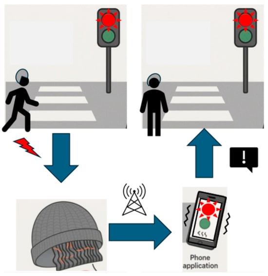
Figure 5.
A schematic representation of a light-sensing array that detects red–green light at a pedestrian crossing and informs the person via a smartphone application. Prepared based on [100].
2.14. SiGe Fiber as a Solar Cell
It is obvious that a SiGe fiber can function as a solar cell only if it contains a built-in electric field to separate photogenerated electron–hole pairs and electrodes to extract current. This requires a p-n (or p-i-n) junction within the fiber, defined current collection pathways, and a geometry compatible with flexing and weaving. The first question is how a p-n junction can be formed in a SiGe fiber? Two such architectures are physically plausible: (i) radial (core–shell) p-n junction (most realistic) and (ii) longitudinal (axial) p-n junction (less practical) (see Table 11). A radial p-n (or p-i-n) junction is the only architecture realistically compatible with a flexible, woven SiGe PV fiber.
Table 11.
Comparison of radial (core–shell) and longitudinal (axial) architecture of p-n junction in SiGe fiber.
The next question is, how do electrodes collect current from a flexible fiber? A functional SiGe fiber solar cell requires two electrically isolated contacts: (i) inner (core) electrode (metallic wire embedded during drawing or selective end-face contact to the doped core) or outer (shell) electrode (conformal transparent conductor (e.g., thin metal mesh; ITO: Indium Tin Oxide; AZO: aluminum-doped zinc oxide); conductive polymer coating for flexibility (e.g., PEDOT:PSS); and thin metal sheath segmented for textile integration. Moreover, instead of two electrically isolated electrodes, a functional SiGe fiber PV device needs low contact resistance to p- and n-type regions, mechanical robustness under bending and weaving, and scalable interconnection between fibers.
As mentioned for radial p-n junction electrode architectures, the core electrode with an outer shell electrode (most common) is preferred, taking into consideration such advantages as continuous current collection along the entire fiber, junction protected inside the fiber, and minimal impact on the bending radius. However, dual-surface electrodes with selective contacts are also possible, where the p-type core is contacted only at the fiber ends or the n-type shell is contacted via continuous surface coating. For this architecture, PV fibers are created via selective etching at fiber ends to expose the core, metal evaporation or paste for end contacts, and a surface shell coated along the fiber length. These solutions exhibited simpler fabrication and are suitable for laboratory demonstration, but less ideal for large textile arrays.
Moreover, to prevent shorting between electrodes, a dielectric buffer layer between the semiconductor and outer electrode (with contact windows) is required, along with a segmented outer electrode to control current pathways. Additionally, polymer cladding for strain relief and insulation is essential. In this case, bending tolerance is maintained by keeping metal layers ultrathin (<100 nm), using ductile metals or polymers and placing brittle layers near the neutral mechanical axis.
And finally, the textile integration includes the fibers acting as individual PV units, an electrical interconnection via weaving, knitting, or conductive threads, or series/parallel connections achieved at fiber ends or junction nodes. Fiber-to-fiber interconnection can be realized via the following: (i) conductive yarns sewn or woven at contact points, (ii) crimping or ultrasonic bonding at fiber ends, and (iii) conductive adhesives for flexible joints. Taking into account circuit configurations, the series connection (increased voltage), parallel connection (increased current), or hybrid textile architectures for power matching can be created.
The proposed device architecture and electrode integration for a SiGe fiber solar cell are presented in Figure 6.
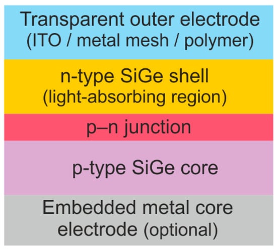
Figure 6.
Graphical architecture of radial SiGe fiber solar cell (cross-section).
A p-type SiGe core is surrounded by an n-type SiGe shell, forming a continuous junction along the fiber length. Photogenerated carriers are separated by the radial built-in electric field. Holes are collected by an inner metal core electrode (embedded during fiber drawing or contacted at the fiber ends), while electrons are collected by a conformal outer electrode (transparent conductive oxide, metal mesh, or conductive polymer) deposited on the fiber surface. Electrical isolation between electrodes is ensured by controlled contact regions and dielectric buffering. The coaxial geometry enables short carrier collection lengths, mechanical robustness under bending, and scalable electrical interconnection when fibers are woven into textile architectures for photovoltaic power generation.
Finally, the question is why radial junctions work best? First, there is a short carrier collection distance (critical for indirect-bandgap SiGe). Second, they are mechanically robust under bending. Third, there is a large junction area per unit length. And fourth, there is standard architecture for nanowire and fiber solar cells.
2.15. Soldier of the Future
Products fabricated from silicon (Si) and germanium (Ge) may serve as the foundation for a new class of multifunctional materials intended for implementation in the concept of the future soldier.
The intrinsic properties of these elements enable the development of fabrics capable of energy generation, physiological monitoring, adaptive camouflage, and environmental protection, while simultaneously integrating multiple systems within a soldier’s exoskeleton and wearable network.
Silicon and germanium, when processed in the form of thin films, nanofibers, or SiGe composites, can form flexible photovoltaic structures integrated into military textiles. Their semiconducting behavior and mechanical flexibility allow for direct energy harvesting on the surface of uniforms and personal equipment (e.g., backpacks or vests), supplying electrical power to an array of on-body systems such as sensors, communication units, ignition devices, and portable electronics. This integration reduces dependence on conventional batteries and enhances operational autonomy in field conditions.
Miniaturized and highly sensitive biosensors, embedded within e-textiles, can monitor vital physiological parameters such as body temperature, heart rate, hydration level, blood pressure, muscle tension, brain activity, and stress or fatigue levels. Another group of sensors may consist of environmental modules capable of detecting ambient temperature, pressure, humidity, or chemical contamination near the soldier, providing real-time situational awareness.
The utilization of Si and Ge in low-power, high-speed microsystems, particularly in conjunction with advances in neurobiology, photonics, and nanotechnology, opens the possibility of developing control units for exoskeletons and human–machine interfaces. Furthermore, the photonic and thermal characteristics of these materials can be employed in multispectral adaptive camouflage systems, designed to dynamically adjust color, gloss, and thermal emissivity to match the surrounding environment. However, the practical implementation of these technologies requires addressing several technical and ethical constraints. The most demanding challenges include the following:
- Durability under field conditions (temperature, humidity, radiation),
- Optimization of energy efficiency and autonomous power supply,
- Ecological and health issues related to germanium processing,
- Biocompatibility of body-assisting systems, and
- Ethical aspects of human–machine integration.
Future research should therefore focus on the following:
- Hybrid SiGe nanofiber architectures,
- Energy recovery systems based on body movement and thermal gradients,
- Biocompatible protective coatings, and
- Cybersecurity of biological and physiological data acquired from soldiers.
The collective potential of silicon and germanium strongly suggests that these materials may become key structural elements of the future soldier’s energetic and sensory infrastructure, combining intelligence, resilience, and autonomy in a single adaptive system. Emerging technologies identified for use by soldiers in tactical and defense operations are presented in Figure 7 [102].
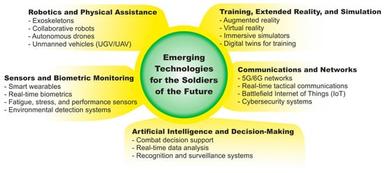
Figure 7.
Emerging technologies identified for use by soldiers in tactical and defense operations, prepared based on [102].
However, the open question remains: how would the proposed PV fibers address key practical issues like washability, durability against abrasion, and connection/interface with other electronic components? Key aspects are summarized in Table 12 [103,104,105,106,107].
Table 12.
Key aspects of practical issues of SiGe used.
Collectively, these advances underline a roadmap for designing practical photovoltaic fibers that meet essential use-case requirements (see Table 13).
Table 13.
Roadmap for designing practical photovoltaic fibers based on SiGe.
Although many advances originate from organic, tribovoltaic, and sensor fiber systems, the engineering principles—washability, abrasion resistance, and robust electrical interfaces—are directly applicable to the development of durable photovoltaic fibers. As SiGe and other high-performance photonic fiber technologies mature, integrating these practical design considerations will be critical to realizing wearable and deployable photovoltaic systems that can withstand daily use and interfacing demands in real environments.
In an era of rapidly advancing artificial intelligence, it is impossible not to ask what specific role is being envisioned for artificial intelligence/machine learning (AI/ML) in optimizing the manufacturing and processing of SiGe fibers? We suggest considering the following aspects, which are included and discussed in Table 14.
Table 14.
What specific role is being envisioned for artificial intelligence/machine learning (AI/ML) in optimizing the manufacturing and processing of SiGe fibers?
Finally, AI enables closed-loop experimentation:
- ➢
- Predict optimal parameters;
- ➢
- Fabricate fibers;
- ➢
- Characterize outcomes;
- ➢
- Retrain models automatically.
This paradigm is particularly valuable for SiGe systems, where experimental costs are high and physical models are incomplete.
In the context of SiGe photovoltaic fibers, AI/ML should be viewed not as a black-box replacement for physics, but as a force multiplier that
- ➢
- Integrates fragmented datasets;
- ➢
- Bridges modeling and experiments;
- ➢
- Accelerates convergence toward scalable fabrication.
When combined with physics-based understanding, AI/ML becomes a strategic enabler for overcoming the remaining technical barriers to long, uniform, and robust SiGe fiber photovoltaics.
3. Conclusions
In summary, it is a fact that in the 21st century, clothing-integrated photovoltaic cells are an interesting option for powering mobile electronic devices. Silicon solar cells have been used with the most promising combination of flexibility and efficiency. The topic of flexible photovoltaics and research is undergoing intensive development worldwide, both from a scientific and an application perspective. Since 2000, research on clothing-integrated solar cells has been regularly presented at trade fairs and exhibitions dedicated to “smart textiles” or “smart clothing”.
From the user’s perspective, photovoltaic clothing should be no different from traditional clothing and should be easy to use, comfortable, and reliable. Furthermore, photovoltaic clothing should be as easy to maintain/clean as any other fabric. The most important and most limiting requirement, however, is the flexibility of the solar cells used in integration with clothing. Current solutions usually result in only one-way bending, not full flexibility like fabric. Furthermore, the user expects the visible elements of the photovoltaic fabric to be visually appealing and blend in with the clothing. Furthermore, connecting cables, charge controllers, and batteries are expected to be invisible, lightweight, and maintenance-free. Photovoltaic fabrics designed for military applications should also meet these requirements. The presented analysis of the advantages and limitations of Si and Ge gives grounds to claim that the world of science is close to producing a feather-light photovoltaic optic fiber, exhibiting mechanical properties typical of Kevlar, enabling power/recharging of portable electric devices while simultaneously protecting against mechanical damage and explosions. Directional solidification of SiGe in a strong thermal gradient will play a key role in achieving this goal.
Author Contributions
Original draft preparation, writing-reviewing and editing, conceptualization, and analyses, A.I. and A.G.; analyses and writing-reviewing, W.P. (Witalis Pellowski), J.M., M.M., M.S., K.A.B., M.Ś., W.P. (Wojciech Przybyl) and P.K. All authors have read and agreed to the published version of the manuscript.
Funding
This research received no external funding.
Data Availability Statement
The authors declare that the data supporting the findings of this study are available within the paper.
Acknowledgments
Authors (A.I. and K.A.B.) are grateful for financial support from Polish National Centre of Research and Development (TECHMATSTRATEG1/347431/14/NCBR/2018).
Conflicts of Interest
The authors declare no conflict of interest.
References
- Sze, S.M.; Li, Y.; Ng, K.K. Physics of Semiconductor Devices; Wiley: New York, NY, USA, 2021. [Google Scholar]
- Kasap, O.; Capper, P. Springer Handbook of Electronic and Photonic Materials, 2nd ed.; Springer: Cham, Switzerland, 2017. [Google Scholar] [CrossRef]
- Madelung, O. Semiconductors: Data Handbook, 3rd ed.; Springer: Berlin, Germany, 2004. [Google Scholar] [CrossRef]
- Theeuwes, R.J.; Kessels, W.M.M.; Macco, B. Surface passivation approaches for silicon, germanium, and III–V semiconductors. J. Vac. Sci. Technol. A 2024, 42, 060801. [Google Scholar] [CrossRef]
- Shen, L.; Teng, C.; Wang, Z.; Bai, H.; Kumar, S.; Min, R. Semiconductor multimaterial optical fibers for biomedical applications. Biosensors 2022, 12, 882. [Google Scholar] [CrossRef]
- Ballato, J.; Hawkins, T.; Foy, P.; Yazgan-Kokuoz, B.; McMillen, C.; Burka, L.; Morris, S.; Stolen, R.; Rice, R. Advancements in semiconductor core optical fiber. Opt. Fiber Technol. 2010, 16, 399–408. [Google Scholar] [CrossRef]
- Peacock, A.C.; Sparks, J.R.; Healy, N. Semiconductor optical fibres: Progress and opportunities. Laser Photonics Rev. 2014, 8, 53–72. [Google Scholar] [CrossRef]
- Gibson, U.J.; Wei, L.; Ballato, J. Semiconductor core fibres: Materials science in a bottle. Nat. Commun. 2021, 12, 3990. [Google Scholar] [CrossRef]
- Park, S.; Loke, G.; Fink, Y.; Anikeeva, P. Flexible fiber-based optoelectronics for neural interfaces. Chem. Soc. Rev. 2019, 48, 1826–1852. [Google Scholar] [CrossRef] [PubMed]
- Yan, W.; Page, A.; Nguyen-Dang, T.; Qu, Y.; Sordo, F.; Wei, L.; Sorin, F. Advanced Multimaterial Electronic and Optoelectronic Fibers and Textiles. Adv. Mater. 2019, 31, 1802348. [Google Scholar] [CrossRef]
- Ren, H.; Shen, L.; Runge, A.F.J.; Hawkins, T.W.; Ballato, J.; Gibson, U.; Peacock, A.C. Low-loss silicon core fibre platform for mid-infrared nonlinear photonics. Light Sci. Appl. 2019, 8, 105. [Google Scholar] [CrossRef] [PubMed]
- Park, S.; Guo, Y.; Jia, X.; Choe, H.K.; Grena, B.; Kang, J.; Park, J.; Lu, C.; Canales, A.; Chen, R.; et al. One-step optogenetics with multifunctional flexible polymer fibers. Nat. Neurosci. 2017, 20, 612–619. [Google Scholar] [CrossRef]
- Zhou, B.; Liu, B.; Zhang, S. The Advancement of 7XXX Series Aluminum Alloys for Aircraft Structures: A Review. Materials 2022, 11, 718. [Google Scholar] [CrossRef]
- Modupeola, D.; Popoola, P. Recent Advances in Joining Technologies of Aluminum Alloys: A Review. Discov. Mater. 2024, 4, 86. [Google Scholar] [CrossRef]
- Erkan, T.; Öztürk, F. AZ31 Magnesium Alloy in the Aerospace Industry: A Review on the Effect of Composition, Microstructure, and Mechanical Properties on Alloy Performance. Kocaeli J. Sci. Eng. 2024, 7, 109–130. [Google Scholar] [CrossRef]
- Jiang, Z.; Hu, B.; Li, Z.; Yao, F.; Han, J.; Li, D.; Zeng, X. A Review of Magnesium Alloys as Structure-Function Integrated Materials. Acta Metall. Sin. (Engl. Lett.) 2024, 37, 1301–1338. [Google Scholar] [CrossRef]
- Wang, H.; Luo, X.C.; Zhang, D.T.; Qiu, C.; Chen, D.L. High-Strength Extruded Magnesium Alloys: A Critical Review. J. Mater. Sci. Technol. 2024, 199, 27–52. [Google Scholar] [CrossRef]
- Tamjid, M.I.; Abtew, M.A.; Kopot, C. Lightweight Textile and Fiber-Reinforced Composites for Soft Body Armor (SBA): Advances in Panel Design, Materials, and Testing Standards. J. Compos. Sci. 2025, 9, 337. [Google Scholar] [CrossRef]
- Lyujia, G. Advancements and Challenges of Smart Materials in Aerospace: Applications, Mechanisms, and Future Prospects. Appl. Comput. Eng. 2025, 147, 7–13. [Google Scholar] [CrossRef]
- Ravi, V. A Comprehensive Review of Advanced Armor Materials and Emerging Technologies in Ballistic Protection for the Next Generation: Factors, Applications, and Future Prospects. Int. Adv. Res. J. Sci. Eng. Technol. 2025, 12, 76–90. [Google Scholar] [CrossRef]
- Jackson, C. Titanium Alloys 2025 Defense—Applications and Alloy Index Signals. AlloyIndex News, 25 September 2025. [Google Scholar]
- Chen, J.; Chen, B. Progress in Additive Manufacturing of Magnesium Alloys: A Review. Materials 2024, 17, 3851. [Google Scholar] [CrossRef] [PubMed]
- Shuvodeep, D.; Zhao, W.; Yuan, Z. Editorial: Lightweight Mechanical and Aerospace Structures and Materials. Front. Mech. Eng. 2024, 10, 1459814. [Google Scholar] [CrossRef]
- Resego, P.; Rangappa, S.M.; Siengchin, S.; Oladijo, O.P.; Ozbakkaloglu, T. Advances in Lightweight Composite Structures and Manufacturing Technologies: A Comprehensive Review. Heliyon 2024, 10, e39661. [Google Scholar] [CrossRef]
- Voron, M.; Skorobagatko, Y.; Tymoshenko, A.; Semenko, A.; Schwab, S.; Smirnov, O. The Potential of Lightweight Steels Application for the Production of Armor Elements for Military Technique. Soc. Dev. Secur. 2024, 14, 106–112. [Google Scholar] [CrossRef]
- Bianchi, I.; Forcellese, A.; Mignanelli, C.; Simoncini, M.; Verdini, T. Development and Life Cycle Analyses of Carbon Fiber Reinforced Polymer Tubular Parts for Metal Replacement in Aerospace Applications. J. Mater. Eng. Perform. 2025, 34, 15324–15335. [Google Scholar] [CrossRef]
- Shetty, R.; Gracias, G.A.; Hegde, A.; Bagade, S.M.; Supriya, J.P.; Shashwat Raman, V. Titanium Alloy and Its Composites: Machinability Review. Int. J. Syst. Assur. Eng. Manag. 2025. [Google Scholar] [CrossRef]
- Coucheron, D.A.; Fokine, M.; Patil, N.; Breiby, D.W.; Buset, O.T.; Healy, N.; Peacock, A.C.; Hawkins, T.; Jones, M.; Ballato, J.; et al. Laser recrystallization and inscription of compositional microstructures in crystalline SiGe-core fibres. Nat. Commun. 2016, 7, 13265. [Google Scholar] [CrossRef]
- Gibson, U.J. Making Silicon-Germanium Core Fibers a Reality. ScienceDaily, 28 October 2016. Available online: https://www.sciencedaily.com/releases/2016/10/161025130101.htm (accessed on 1 December 2025).
- Jens, K.; Jörg, B.; Katrin, W.; Claudia, A.; Zhiwen, P.; Sonja, U.; Kay, S.; Hartmut, B. Diffusion and Interface Effects during Preparation of All-Solid Microstructured Fibers. Materials 2014, 7, 6879. [Google Scholar] [CrossRef]
- Gumennik, A.; Levy, E.C.; Grena, B.; Hou, C.; Rein, M.; Abouraddy, A.F.; Joannopoulos, J.D.; Fink, Y. Confined in-fiber solidification and structural control of silicon and silicon–germanium microparticles. Proc. Natl. Acad. Sci. USA 2017, 114, 7240–7245. [Google Scholar] [CrossRef] [PubMed]
- Shanks, W.C.P., III; Kimball, B.E.; Tolcin, A.C.; Guberman, D.E. Germanium and Indium. In Critical Mineral Resources of the United States-Economic and Environmental Geology and Prospects for Future Supply; U.S. Geological Survey: Reston, VA, USA, 2017; Chapter I; Volume 1022, pp. I1–I27. [Google Scholar] [CrossRef]
- USGS MYB 1994-2017, U.S. Geological Survey, Minerals Yearbook 1994–2017: Germanium. Available online: https://www.usgs.gov/centers/nmic/germanium-statistics-and-information (accessed on 1 December 2025).
- European Commission. Study on the Review of the List of Critical Raw Materials—Critical Raw Materials Factsheets; Publications Office of the European Union: Luxembourg, 2020. [Google Scholar] [CrossRef]
- Patel, M.; Karamalidis, A.K. Germanium: A review of its US demand, uses, resources, chemistry, and separation technologies. Sep. Purif. Technol. 2021, 275, 118981. [Google Scholar] [CrossRef]
- Guberman, D.E. Germanium: U.S. Geological Survey Mineral Commodity Summaries; U.S. Geological Survey: Reston, VA, USA, 2013; pp. 64–65. Available online: https://minerals.usgs.gov/minerals/pubs/commodity/germanium/mcs-2013-germa.pdf (accessed on 1 December 2025).
- European Commission: Directorate-General for Internal Market, Industry, Entrepreneurship and SMEs. Study on the EU’s List of Critical Raw Materials (2020)—Final Report; Publications Office of the European Union: Luxembourg, 2020; Available online: https://data.europa.eu/doi/10.2873/11619 (accessed on 1 December 2025).
- Rosenberg, E. Germanium: Environmental occurrence, importance and speciation. Rev. Environ. Sci. Bio/Technol. 2009, 8, 29–57. [Google Scholar] [CrossRef]
- Yandem, G.; Jabłońska-Czapla, M. Review of indium, gallium, and germanium as emerging contaminants: Occurrence, speciation and evaluation of the potential environmental impact. Arch. Environ. Prot. 2024, 50, 84–99. [Google Scholar] [CrossRef]
- Haller, E.E. Germanium: From its discovery to SiGe devices. Mater. Sci. Semicond. Process. 2006, 9, 408–422. [Google Scholar] [CrossRef]
- Wilson, G.M.; Al-Jassim, M.; Metzger, W.K.; Glunz, S.W.; Verlinden, P.; Xiong, G.; Mansfield, L.M.; Stanbery, B.J.; Zhu, K.; Yan, Y.; et al. The 2020 photovoltaic technologies roadmap. J. Phys. D Appl. Phys. 2020, 53, 493001. [Google Scholar] [CrossRef]
- Curtolo, D.C.; Friedrich, S.; Friedrich, B. High Purity Germanium, a Review on Principle, Theories and Technical Production Methodologies. J. Cryst. Process Technol. 2017, 7, 65–84. [Google Scholar] [CrossRef]
- Srivastava, R.R.; Ilyas, S. Harnessing Germanium from Industrial Residues and Electronic Waste for a Sustainable Energy Future. Green Chem. 2025, 27, 14744–14768. [Google Scholar] [CrossRef]
- Rudnik, E. Challenges and Opportunities in Hydrometallurgical Recovery of Germanium from Coal By-Products. Molecules 2025, 30, 1695. [Google Scholar] [CrossRef]
- Current State of Germanium Supply. Quest Metals Blog, 18 June 2025.
- Jabłońska-Czapla, M.; Grygoyć, K.; Rachwał, M.; Fornalczyk, A.; Willner, J. Assessment of Contamination, Mobility and Application of Selected Technology-Critical Elements as Indicators of Anthropogenic Pollution of Bottom Sediments. Environ. Sci. Pollut. Res. 2024, 31, 49694–49714. [Google Scholar] [CrossRef]
- Cai, J.; Zhang, B.; Dang, J.; Zhao, Y.; Liang, D.; Xie, Q.; Fan, M.; Liu, J. Insights into critical metal element migration and enrichment in coal gasification. RSC Adv. 2025, 15, 8169–8179. [Google Scholar] [CrossRef]
- Pitzke, K.; Wippich, C.; Woznica, A.; Hebisch, R.; Brock, T.; Hartwig, A.; MAK Commision. Germanium—Determination of germanium and its non-volatile inorganic compounds in workplace air using inductively coupled plasma mass spectrometry (ICP-MS). MAK Collect. Occup. Health Saf. 2024, 9, Doc041. [Google Scholar] [CrossRef]
- Wölfer, E.; Burkhardt, C.; Kleine, T. Germanium stable isotope measurements by double-spike MC-ICPMS. J. Anal. At. Spectrom. 2025, 40, 1023–1036. [Google Scholar] [CrossRef]
- Alguacil, F.J.; Robla, J.I. Some Recent Advances in Germanium Recovery from Various Resources. Metals 2024, 14, 559. [Google Scholar] [CrossRef]
- Smith, A.J.; Brown, L.M.; Lee, H.K. Elemental Speciation Update: Germanium. J. Anal. At. Spectrom. 2024, 39, 205–217. [Google Scholar] [CrossRef]
- Zohar, I.; Ganem, H.E.; DiSegni, D.M.; Jonas-Levi, A. Effect of Sewage Sludge and Digestate from Anaerobic Fermentation on the Accumulation of Cadmium (Cd), Gallium (Ga), Germanium (Ge), and Rare Earth Elements (REEs) in Soil and Uptake by Plants with Different Nutrition Strategies. Front. Environ. Sci. 2025, 13, 1628175. [Google Scholar] [CrossRef]
- López-Urzúa, S.; Derry, L.A.; Bouchez, J. Quantifying the Agricultural Footprint on the Silicon Cycle: Insights from Silicon Isotopes and Ge/Si Ratios. Biogeosciences 2025, 22, 6067–6095. [Google Scholar] [CrossRef]
- Montserrat, F.; Rodríguez-Murillo, J.-C. Germanium in the Environment: Current Knowledge and Identification of Gaps. Soil Environ. Health 2025, 3, 100132. [Google Scholar]
- Villani, M.; Hirst, C.; du Bois d’Aische, E.; Thomas, M.; Lundin, E.; Giesler, R.; Mörth, C.-M.; Opfergelt, S. Lengthening of Biogeochemical Processes during Winter in Degraded Permafrost Soils. Geochem. Perspect. Lett. 2025, 34, 36–42. [Google Scholar] [CrossRef]
- Dobrzyński, D.; Tetfejer, K.; Stępień, M.; Karasiński, J.; Tupys, A.; Słaby, E. Geochemistry of Germanium in Thermal Waters of the Jelenia Góra Geothermal System (Sudetes, Poland): Solute Relationships and Aquifer Mineralogy. Ann. Soc. Geol. Pol. 2023, 93, 323–344. [Google Scholar] [CrossRef]
- Huston, D.L.; Bastrakov, E. Germanium, Indium, Gallium and Cadmium in Zinc Ores. Aust. J. Earth Sci. 2024, 71, 1125–1155. [Google Scholar] [CrossRef]
- Fraunhofer Institute for Solar Energy Systems, ISE. Photovoltaics Report; ISE: Freiburg, Germany, 2023. [Google Scholar]
- Di Sabatino, M.; Hendawi, R.; Garcia, A.S. Silicon Solar Cells: Trends, Manufacturing Challenges, and AI Perspectives. Crystals 2024, 14, 167. [Google Scholar] [CrossRef]
- Green, M.A.; Dunlop, E.D.; Hohl-Ebinger, J.; Yoshita, M.; Kopidakis, N.; Bothe, K.; Hinken, D.; Rauer, M.; Hao, X. Solar cell efficiency tables (Version 60). Prog. Photovoltaics Res. Appl. 2022, 30, 687–701. [Google Scholar] [CrossRef]
- Tuan Le, A.H.; Basnet, R.; Yan, D.; Chen, W.; Nandakumar, N.; Duttagupta, S.; Seif, J.P.; Hameiri, Z. Temperature-dependent performance of silicon solar cells with polysilicon passivating contacts. Sol. Energy Mater. Sol. Cells 2021, 225, 111020. [Google Scholar] [CrossRef]
- Green, M.A. General temperature dependence of solar cell performance and implications for device modelling. Prog. Photovolt. Res. Appl. 2003, 11, 333–340. [Google Scholar] [CrossRef]
- Osterwald, C.R.; Campanelli, M.; Moriarty, T.; Emery, K.A.; Williams, R. Temperature-dependent spectral mismatch corrections. IEEE J. Photovolt. 2015, 5, 1692–1697. [Google Scholar] [CrossRef]
- Müllejans, H.; Wagner, T.; Merli, F.; Jäger-Waldau, A.; Dunlop, A.E.D. Changes in spectra response with temperature and irradiance intensity. Thin Solid Film. 2004, 451–452, 145–151. [Google Scholar] [CrossRef]
- Jordan, D.C.; Kurtz, S.R.; Van Sant, K.; Newmiller, J. Compendium of photovoltaic degradation rates. Prog. Photovolt. Res. Appl. 2016, 24, 978–989. [Google Scholar] [CrossRef]
- Arruti, O.A.; Virtuani, A.; Ballif, C. Long-term performance and reliability of silicon heterojunction solar modules. Prog. Photovolt. Res. Appl. 2023, 31, 664–677. [Google Scholar] [CrossRef]
- Louwen, A.; van Sark, W.; Schropp, R.; Faaij, A. A cost roadmap for silicon heterojunction solar cells. Sol. Energy Mater. Sol. Cells 2016, 147, 295–314. [Google Scholar] [CrossRef]
- Mdallal, A.; Yasin, A.; Mahmoud, M.; Ali Abdelkareem, M.; Hai Alami, A.; Ghani Olabi, A. A comprehensive review on solar photovoltaics: Navigating generational shifts, innovations, and sustainability. Sustain. Horiz. 2025, 13, 100137. [Google Scholar] [CrossRef]
- McCann, M.J.; Catchpole, K.R.; Weber, K.J.; Blakers, A.W. A review of thin-film crystalline silicon for solar cell applications. Part 1: Native substrates. Sol. Energy Mater. Sol. Cells 2001, 68, 135–171. [Google Scholar] [CrossRef]
- Liu, W.; Liu, Y.; Yang, Z.; Xu, C.; Li, X.; Huang, S.; Shi, J.; Du, J.; Han, A.; Yang, Y.; et al. Flexible solar cells based on foldable silicon wafers with blunted edges. Nature 2023, 617, 717–723. [Google Scholar] [CrossRef]
- Yadav, N.; Khare, A. Resolving interfacial challenges in perovskite solar cells: From defect control to energy band optimization. Surf. Interfaces 2025, 56, 105593. [Google Scholar] [CrossRef]
- Sun, G.; Chang, F.; Soref, R.A. High efficiency thin-film crystalline Si/Ge tandem solar cell. Opt. Express 2010, 18, 3746–3753. [Google Scholar] [CrossRef]
- Kayes, B.M.; Atwater, H.A.; Lewis, N.S. Comparison of the device physics principles of planar and radial p–n junction nanorod solar cells. J. Appl. Phys. 2005, 97, 114302. [Google Scholar] [CrossRef]
- Stoppa, M.; Chiolerio, A. Wearable Electronics and Smart Textiles: A Critical Review. Sensors 2014, 14, 11957–11992. [Google Scholar] [CrossRef] [PubMed]
- National Research Council. Energy-Efficient Technologies for the Dismounted Soldier; The National Academies Press: Washington, DC, USA, 1997; Available online: https://www.nationalacademies.org/read/5905/chapter/1 (accessed on 1 December 2025).
- Schubert, M.B.; Werner, J.H. Flexible solar cells for clothing. Mater. Today 2006, 9, 42–50. [Google Scholar] [CrossRef]
- Gui, H.; Zhang, Z.; Blalock, B.J. Review of Power Electronics Components at Cryogenic Temperatures. IEEE Trans. Power Electron. 2020, 35, 5144–5156. [Google Scholar] [CrossRef]
- Aishwarya, K.; Lakshmi, B. TCAD simulation study of heavy ion radiation effects on hetero junctionless tunnel field effect transistor. Sci. Rep. 2024, 14, 7643. [Google Scholar] [CrossRef]
- Lide, D.R. (Ed.) CRC Handbook of Chemistry and Physics; Internet Version 2005; CRC Press: Boca Raton, FL, USA, 2005; pp. 4–28. Available online: https://books.google.pl/books?id=q2qJId5TKOkC&printsec=frontcover&hl=pl&source=gbs_ge_summary_r&cad=0#v=onepage&q&f=false (accessed on 1 December 2025).
- Olesinski, R.W.; Abbaschian, G.J. The Ge-Si (Germanium-Silicon) System. Bull. Alloy Phase Diagr. 1984, 5, 180–183. [Google Scholar] [CrossRef]
- Soma, T.; Matsuo, H.; Katoh, T. The Heat of Mixing in Liquid Si-Ge, Si-Sn, and Ge-Sn Mixtures. Phys. Status Solidi (B) 1981, 106, K5–K7. [Google Scholar] [CrossRef]
- Soma, T.; Iwanami, H.; Matsuo, H. Phase Transition under Pressure of Si-Ge Solid Solutions. Solid State Commun. 1982, 42, 469–471. [Google Scholar] [CrossRef]
- Soma, T.; Iwanami, H.; Matsuo, H. Equation of State of Si-Ge Solid Solution. Phys. Status Solidi (B) 1982, 110, 75–79. [Google Scholar] [CrossRef]
- Soma, T.; Iwanami, H.; Matsuo Kagaya, H. Pressure-Volume Relation Under High Pressure for Si-Ge Solid Solution. Phys. Status Solidi (B) 1982, 111, K23–K26. [Google Scholar] [CrossRef]
- Mogaddam, N.A.P.; Alagoz, A.S.; Yerci, S.; Turan, R.; Foss, S.; Finstad, T.G. Phase separation in SiGe nanocrystals embedded in SiO2 matrix during high temperature annealing. J. Appl. Phys. 2008, 104, 124309. [Google Scholar] [CrossRef]
- Gotoh, R.; Fujiwara, K.; Yang, X.; Koizumi, H.; Nozawa, J.; Uda, S. Formation mechanism of cellular structures during unidirectional growth of binary semiconductor Si-rich SiGe materials. Appl. Phys. Lett. 2012, 100, 021903. [Google Scholar] [CrossRef]
- Littlejohns, C.G.; Nedeljkovic, M.; Mallinson, C.F.; Watts, J.F.; Mashanovich, G.Z.; Reed, G.T.; Gardes, F.Y. Next generation device grade silicon-germanium on insulator. Sci. Rep. 2015, 5, 8288. [Google Scholar] [CrossRef]
- Su, H.; Hurd Price, C.-A.; Jing, L.; Tian, Q.; Liu, J.; Qian, K. Janus particles: Design, preparation, and biomedical applications. Mater. Today Bio 2019, 4, 100033. [Google Scholar] [CrossRef]
- Sun, Y.; Thompson, S.E.; Nishida, T. Physics of strain effects in semiconductors and metal-oxide-semiconductor field-effect transistors. J. Appl. Phys. 2007, 101, 104503. [Google Scholar]
- Healy, N.; Mailis, S.; Bulgakova, N.M.; Sazio, P.J.A.; Day, T.D.; Sparks, J.R.; Cheng, H.Y.; Badding, J.V.; Peacock, A.C. Extreme electronic bandgap modification in laser-crystallized silicon optical fibres. Nat. Mater. 2014, 13, 1122–1127. [Google Scholar] [CrossRef] [PubMed]
- Mehringer, C.; Wagner, R.; Jakuttis, T.; Butz, B.; Spiecker, E.; Peukert, W. Gas phase synthesis of anisotropic silicon germanium hybrid nanoparticles. J. Aerosol Sci. 2014, 67, 119–130. [Google Scholar] [CrossRef]
- Avci, H.; Hassanin, A.; Hamouda, T.; Kiliç, A. High performance fibers: A review on current state of art and future challenges. J. Eng. Archit. Fac. Eskiseh. Osman. Univ. 2019, 27, 130–155. [Google Scholar] [CrossRef]
- Lyu, J.; Liu, Z.; Wu, X.; Li, G.; Fang, D.; Zhang, X. Nanofibrous Kevlar Aerogel Films and Their Phase-Change Composites for Highly Efficient Infrared Stealth. ACS Nano 2019, 13, 2236–2245. [Google Scholar] [CrossRef]
- Kerr, M.; Chawla, N.; Chawla, K. The cyclic fatigue of high-performance fibers. JOM 2005, 57, 67–71. [Google Scholar] [CrossRef]
- Hearle, J.W.S. High-Performance Fibres; Woodhead Publishing: Cambridge, UK, 2001; ISBN 9781855735392 (hbk), 9781855737549 (ebk). [Google Scholar]
- Substituent Effects. 2019. Available online: http://www.mhhe.com/physsci/chemistry/carey/student/olc/graphics/carey04oc/ref/ch12substituenteffects.html (accessed on 1 December 2025).
- World Health Organization. Ultraviolet Radiation and Health. 2019. Available online: http://www.who.int/uv/uv_and_health/en/ (accessed on 1 December 2025).
- Lei, X.; Xiao, K.; Wu, X.; Huang, C. Dynamic Mechanical Properties of Several High-Performance Single Fibers. Materials 2021, 14, 3574. [Google Scholar] [CrossRef]
- Kuryliuk, V.; Popiuk, K.; Belyavina, N.; Kuryliuk, A. Atomistic study of mechanical properties of SiGe hollow-core nanowires. Mater. Res. Express 2025, 12, 085006. [Google Scholar] [CrossRef]
- Wang, Z.; Wang, Z.; Li, D.; Yang, C.; Zhang, Q.; Chen, M.; Gao, H.; Wei, L. High-quality semiconductor fibres via mechanical design. Nature 2024, 626, 72–78. [Google Scholar] [CrossRef] [PubMed]
- Rahmana, M.H.; Haque Chowdhurya, E.; Islam, M.M. Understanding Mechanical Properties and Failure Mechanism of Germanium-Silicon Alloy at Nanoscale. arXiv 2020, arXiv:2004.13445. [Google Scholar] [CrossRef]
- Luna, E.; Catana, P.; Calderon, J.; Ponce, M. Advances in Technologies for the Soldiers of the Future. Athenea J. 2025, 6, 29–42. [Google Scholar] [CrossRef]
- Fan, B.; Liu, G.; Dai, Y.; Dong, Z.; Luan, R.; Gong, L.; Zhang, Z.; Wang, Z.L.; Zhang, C. A wearable DC tribovoltaic power textile woven by P/N-type organic semiconductor fibers. Energy Environ. Sci. 2024, 17, 8621–8632. [Google Scholar] [CrossRef]
- Kim, H.; Choi, J.G.; Oh, T.; Lee, I.; Lee, H.; Jin, H.; Hong, C.-H.; Kim, H.J.; Kim, T.-W.; Park, S. Waterproof and conductive tough fibers for washable e-textile. npj Flex. Electron. 2025, 9, 28. [Google Scholar] [CrossRef]
- Stachewicz, U. Emerging Trends in Electrospinning: From Nanofibers to Applications. Macromol. Rapid Commun. 2025, 46, 2500394. [Google Scholar] [CrossRef] [PubMed]
- Wang, X.; Chen, G.; Cai, L.; Li, R.; He, M. Weavable Transparent Conductive Fibers with Harsh Environment Tolerance. ACS Appl. Mater. Interfaces 2021, 13, 7. [Google Scholar] [CrossRef] [PubMed]
- Bai, X.; Zhu, M.; Pan, S. Fiber electronics for wearable interactive systems. J. Mater. Chem. C 2025, 13, 17396–17415. [Google Scholar] [CrossRef]
Disclaimer/Publisher’s Note: The statements, opinions and data contained in all publications are solely those of the individual author(s) and contributor(s) and not of MDPI and/or the editor(s). MDPI and/or the editor(s) disclaim responsibility for any injury to people or property resulting from any ideas, methods, instructions or products referred to in the content. |
© 2026 by the authors. Licensee MDPI, Basel, Switzerland. This article is an open access article distributed under the terms and conditions of the Creative Commons Attribution (CC BY) license.