Abstract
An MMC is widely applied to the HVDC power transmission system. With a large number of insulated gate bipolar transistors (IGBTs) utilized in MMC-HVDC converter stations, an extremely complicated EM environment is generated due to the dv/dt and di/dt during the IGBT switching process. A magnetic field simulation model is proposed to calculate the magnetic field generated by a 4.5 kV/5 kA IGBT-based MMC submodule under the DPT, with the dynamic switching behavior of IGBTs considered. Firstly, a behavior model of 4.5 kV/5 kA IGBTs is built with the help of commercial software. To validate its effectiveness, a DPT simulation model is built. A comparison between the simulation result and the measured data is performed. Finally, a quasi-static Maxwell model is utilized to approximate the near field caused by the current Ic of the DPT. The simulation result of the magnetic field strength at the point near the gate driver PCB is verified by the measurement data. The proposed magnetic field simulation model can help to analyze the EMI behavior and EMI design for MMC-HVDC submodules under DPT.
1. Introduction
Modular multilevel converters have been widely applied to many HVDC projects worldwide due to their advantages of bidirectional power transmission, commutation failure-less problems, good power quality, and high reliability [1]. The reliability of HVDC power transmission has become more and more significant, and it is vital for the safety and steady operation of HVDC systems [2,3]. Nowadays, most research on MMC-HVDC is focused on topologies, modulation and control strategies, circulating current suppression, and capacitor voltage balance [4]. However, EMI problems are rarely considered [5]. Submodules are the core components of MMC-HVDC, and the reliability is important to the safe operation of converter valves. According to the failure statistics of converter valves in typical VSC-HVDC projects in China, the failure rate caused by IGBTs accounts for 2% of all the failure cases. Meanwhile, the failure rate caused by the secondary equipment, like the drive unit, control unit, and communication unit, is over 80% [2,4]. With the development of wideband gap devices towards higher power density, the di/dt and dv/dt will be even more harsh, and the influence of EMI on the secondary equipment will be much more severe [6]. With the utilization of 4.5 kV/5 kA and 6.5kV/3kA IGBTs in the UHVDC projects, the di/dt and dv/dt may be even more harsh.
As it is known, EMI includes three key elements: EMI sources, propagation paths, and sensitive devices. Usually, di/dt and dv/dt of the power electronics switches in the submodule, such as IGBTs, are considered to be the primary sources of EMI. The values of dv/dt and di/dt during the switching period of the IGBT in MMC are much higher, and the maximum dv/dt of the IGBT can be 1.8 kV/μs [7]. The over-voltage and ringing induced by the di/dt noise could cause high-voltage stress, extra loss, and severe radio frequency emission problems. Spurious gate voltage, crosstalk issues, and high common mode (CM) voltage generated by the high dv/dt noise may lead to the false trigger of gate drive ICs [7,8]. Regarding the MMC EMI source suppression techniques, research on modulation strategies is conducted. By optimizing the pulse width modulation (PWM) strategy, low-frequency EMI noise (from 150 kHz to several megahertz) can be reduced without adding any passive equipment. By adjusting the frequency, amplitude, and phase of the carrier, spread-spectrum technology, an emerging method, can be used to optimize the PWM strategy. There are three types of spread-spectrum technology: random PWM, periodic PWM, and programmed PWM [9]. In [10], a space spread-spectrum strategy is put forward to relieve EMI harmonic surges by making the carrier frequency of each submodule different while keeping carrier frequencies fixed instead of changing with time. Sun verified that nearest-level modulation performs better than phase-shifting carrier pulse width modulation in EMI suppression [11]. In the aspect of conducted EMI reduction measures, several modulation-based methods to reduce the common-mode (CM) voltage of the output middle point are proposed in [4,5,10,12,13,14].
According to the propagation paths, EMI could be divided into conducted EMI and radiated EMI. As for the mechanisms of conducted EMI of MMC, research has been undertaken. The common-mode voltage of MMC with the nearest-level modulation scheme is analyzed in [14]. The scheme proposed can mitigate the common-mode voltage and common-mode current caused by the modulation without causing obvious power-quality degradation and the utilization of the DC bus. In [15], a piecewise approximation method is adopted to simulate the switching voltage and current of the real device, which can promote the accuracy of high-frequency EMI modeling. In [16], the GPU’s massive parallelism technique was employed to simulate the conducted EMI characteristics of the MMC-HVDC system. By separating all the two-port networks and MMC SMs, a fine-grained network is obtained. In the aspect of EMI modeling, Chen built a CM EMI model for the submodule auxiliary power supply [14]. EMI filters, active gate drivers, and snubber circuits are techniques utilized to reduce high-frequency EMI from the source (up to 30 MHz) [10].
Studies on radiated EMI of MMC-HVDC are also performed. Measurements of the radiated electric field characteristics for a multi-terminal MMC-HVDC converter system are studied in [17]. The converter valve tower is modeled as a complex antenna structure, and the calculation of near-field radiation intensity for the converter valve tower is performed in commercial software [18]. In [19], a novel method, which combines the method of moments with antenna theory to analyze the radiated EM disturbance of the VSC-HVDC converter system, is presented. With the utilization of a large number of IGBTs in MMC, for instance, the maximum number of submodules per arm has exceeded 400 [5], which brings many potential EMI sources into the power system and forms an extremely complex EM environment [20]. This complex EMI source may disturb normal operations of components of the secondary system, which are vulnerable to EM disturbance, such as sensors, control units, and driver units [4,5]. Research on the radiated EMI of the converter valve only is commonly made. It is intuitively believed and verified that the gate driver PCB is strongly influenced by the dv/dt and di/dt generated by the closest IGBTs, and the magnetic field disturbance contributed by its nearest submodel can be up to about 90% [21]. Generally, the gate-driver PCB is recognized to experience the most critical EMI environment under the double pulse test (DPT). However, studies on the EMI environment of submodules under DPT have not examined IGBTs up to 4.5 kV/5 kA, which may lead to operation failure during the switching period and deteriorate the safety operation of the MMC-HVDC converter valve.
Apparently, EMI problems have been studied by researchers. However, most of them are not press-pack structures used in MMC-HVDC projects. The maximum rated value of the DC collector current is up to 5 kA, which is the highest in the available commercial IGBT products. For such a new device, its operating condition, such as the current handled, is different compared to other IGBTs. The di/dt and the EMI caused by it for such an IGBT are necessary to be studied since they are quite important and expensive for MMC-HVDC submodules and valve stations. Since the near-field generated by the IGBT is often considered to have a strong influence on the electromagnetic-sensitive component, a near-field simulation model is proposed to accurately calculate the near-field caused by the di/dt during the switching period by combining the dynamic switching behavior of IGBTs with the quasi-static Maxwell model. The organization of this paper is shown as follows. Firstly, the dynamic behavior of 4.5 kV/5 kA IGBTs and freewheeling diodes is introduced during the switching period. Then, this dynamic behavior model is simulated by using commercial software, and it is validated by using DPT. Finally, a near-field model is built by combining the dynamic behavior model and the quasi-static Maxwell equations to approximate the full-wave Maxwell equations, and its effectiveness is verified by measuring the magnetic field strength generated by the DPT.
2. Behavior Model of 4.5 kV/5 kA IGBTs and Freewheeling Diodes
A schematic diagram of the main circuit of a three-phase MMC is shown in Figure 1a. A typical MMC-HVDC usually consists of three phases, each including a lower and an upper arm. A series of submodules is interconnected to form an MMC-HVDC valve, and a multilevel voltage waveform is generated at its terminals. The submodules can be interconnected according to the application’s requirement, such as the DC to three-phase topology as shown in Figure 1a, which is widely used in HVDC power transmission. For a real MMC-HVDC project, it may have more than 200 submodules per arm to generate a high-quality sinusoidal voltage waveform by selectively inserting or bypassing SMs via switching actions. The stepped output voltage, formed by aggregating SM capacitor voltages, approximates a sine wave with minimal harmonic distortion. A typical architecture of an MMC valve tower is shown in Figure 1b.
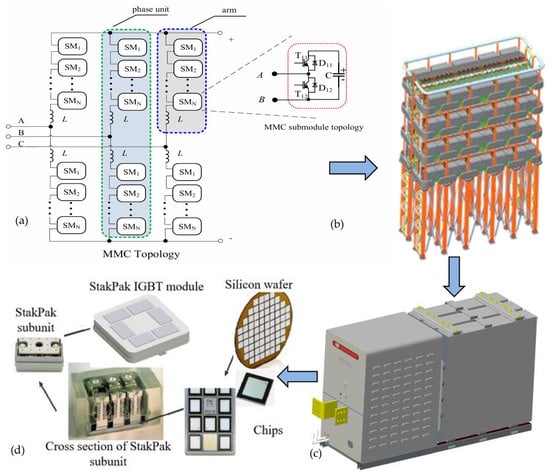
Figure 1.
MMC-HVDC topology (a), the architecture of an MMC valve tower (b), a typical submodule (c), and IGBT internal structure (d).
A typical submodule, illustrated in Figure 1c, usually consists of the primary part, such as IGBTs, capacitors, and diodes, and the secondary part, such as the drive unit, power supply unit, and control unit. Submodules are the basic and key components of an MMC valve. A variety of topologies of the submodule, such as the half-bridge, full-bridge, cross-connected submodule, and so on, have been proposed and studied. The half-bridge submodule has been widely adopted nowadays for its cost-effective topology. As one of the key components of MMC submodules, IGBTs play an important role in the DC and AC energy conversion. As it is mentioned, the high dv/dt and di/dt during the switching period of IGBTs are the main sources of EMI. Therefore, an accurate IGBT and its recovery diode model are essential for the EMI analysis. The internal structure of a 4.5 kV/5 kA press-pack IGBT is shown in Figure 1d. It is shown that the details of the internal structure of the press-pack IGBT are very complex.
To accurately model the electrical behavior of the IGBT is quite difficult since all the geometry and material parameters are needed and hard to acquire. The model of semiconductor devices, such as IGBT, involves the drift and diffusion of carriers, which is usually formulated by the ambipolar diffusion equation (ADE). It is quite cumbersome to solve this equation, and some of the parameters need to be extracted from the device’s transient waveforms; dedicated characteristic test equipment is also needed. Here, an advanced dynamic IGBT model and a dynamic freewheeling diode behavior model are adopted [16,22,23].
The data needed for building this behavior model of the 4.5 kV/5 kA IGBT and its freewheeling diode during the turn-on/turn-off period can be acquired from the manufacturer’s datasheet, which can be easily obtained. The behavior model utilized here is characterized by the parasitic capacitances and inductances, as shown in Figure 2. These electrical components of this behavior model can be extracted from information such as the IGBTs’ transfer characteristics and output characteristics [16,22,23].
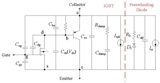
Figure 2.
Equivalent circuit of the IGBT behavior model.
2.1. IGBT Model
The static characteristics of IGBT can be modeled by using a bipolar junction transistor (BJT) and a metal oxide semiconductor field effect transistor (MOSFET) in a Darlington connection. The dynamic characteristic during the switching process can be represented by the junction capacitance and diffusion capacitance. The output characteristics for the linear and saturation regions of the MOSFET can be modeled by the Shichman–Hodges model, which can be formulated by Equations (1)–(4).
Saturation voltage,
Saturation current,
The drain current within the linear region (VDS < VGS),
The drain current for the saturation region (VDS ≥ VGS),
Here, KLM is the model parameter to be identified. Usually, the drain current ID is equal to the source current Is.
The forward conduction characteristics of the BJT considered here can be formulated by,
In general, Isat_BJT is equal to ID. VT is the temperature voltage, which can be solved by
VT = k∙(Tjnc + 273)/q
As is known, the transient switching characteristics of IGBTs are primarily influenced by the junction capacitances between terminals. The corresponding capacitance for the p-n junction under the positive-biased enhanced state and negative-biased depleted state is shown as follows.
Enhanced state ():
depleted state ():
Here,
For Ceg, Cdg, Cec, Cds, Cgs, VJCT is Veg, Vdg, Vec, Vds, and Vgs, respectively.
The diffusion capacitance within the freewheeling diode is modeled using the same approach can be defined as
Here, i(t) is equal to ib and id for Cbe and Cdf, respectively.
The switch-off current edge is affected by parameters τtail and δtail because δtail shapes the falling edge, while τtail is the duration time. The injected current Itail, at load current Iload is expressed as
2.2. Diode Model
The freewheeling diode is modeled as an ideal diode in series with a current-dependent resistor. The static current of the freewheeling diode and resistor can be given by the following equations,
The waveform of the diode reverse recovery current can be defined as a form of piece-wise function with five sections, as depicted in Figure 3. These sections are connected in a way to maintain differentiability at the boundary from one region to the other. The maximum current Irr_max, is formulated by
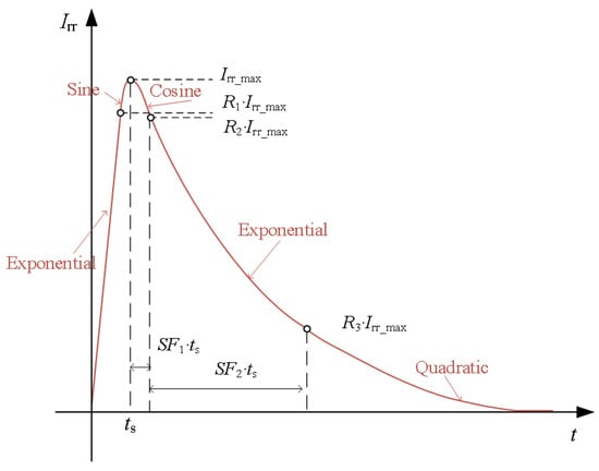
Figure 3.
Reverse recovery waveform of a diode.
Time ts can be calculated from the reverse recovery charge Qrr and the form factors when Irr max is reached. The IGBTs’ transfer characteristics and output characteristics used for this behavior model determination are given in Figure 4a and Figure 4b, respectively.
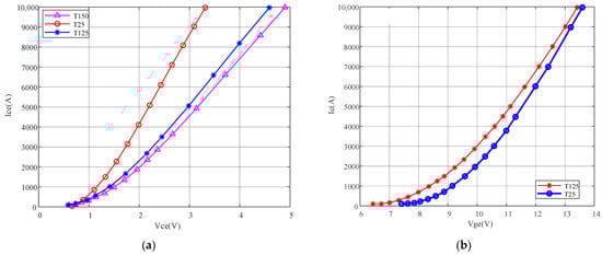
Figure 4.
Typical output characteristics, chip level (a); typical transfer characteristics, chip level (b).
As for the dynamic properties of the IGBT, they can be determined by the turn-on/turn-off energy and turn-on/turn-off time. These values are set to be the reference values for optimization during the electrical components’ extraction process of this behavior model. The optimal results are listed in Table 1, and the overall error is less than 10%.

Table 1.
Comparison of the modeling results with the datasheet values.
3. Double Pulse Test Simulation and Validation
As mentioned above, it consists of several hundred submodules for a real MMC valve tower. An approximated sine wave can be obtained. By measuring the current at different positions of an MMC assembly shown in Figure 5a, we can observe its characteristics. From Figure 5b, it can be observed that current i1 through the phase leg is close to a sine wave. However, the waveform of the current through the IGBT is quite different from i1. It has many square-like waves. Apparently, the di/dt of these waves is much larger than that of a sin wave. Hence, a DPT is adopted here to model these square-like waves.
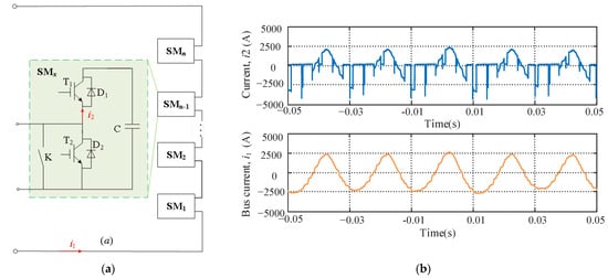
Figure 5.
Current measuring positions (a) and current vs. time (b) of an MMC submodule.
Firstly, to validate the adopted behavior model of the IGBT, a DPT is conducted. The schematic diagram of a DPT for half-bridge topology is shown in Figure 6a. A DPT enables IGBTs to be switched on and off at different current levels. By adjusting the switching times (t0~t1, t1~t2, t2~t3) in Figure 6b, the turn-on and turn-off waveforms, such as Vge, Vce, and Ic, of the IGBTs can be controlled and measured over the full range of operating conditions. It is a standard method for measuring switching parameters, such as turn-on energy, turn-off energy, turn-on time, turn-off time, leakage inductance, reverse recovery current, and so on. To be noticed, IGBT T1 is always set to be in the OFF state during the whole process for the half-bridge submodule. Before t0, the capacitor Cin is charged. At t0, a positive value of Vge (+15 V) is applied, and current Ic goes through Cin-Lind-T2-Cin, which is shown in Figure 6a with a red solid line. During t0~t1, current Ic increases with time, and Ic = IL, IRR = 0, and Vce = 0. At t1, a negative value of Vge (−15 V) is applied. Then, during t1~t2, current IL goes through Lind-D1-Lind, which is illustrated as the green line in Figure 6a, and Ic = 0.
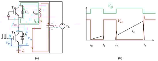
Figure 6.
Schematic diagram of DPT for half bridge (a) and typical waveform of dual pulse test for Vge, Vce, and Ic (b).
The turn-off current is about 10 kA at t3 for the DPT. The pre-charged voltage for the capacitor, Cin, is about 3200 V at t0. The inductance, Lind, is 56 μH, and the capacitance, Cin, is 27 mF. The resistance for the driver during the turn-on state is 1.3Ω, while the resistance for the turn-off is 7.8Ω. The stray inductance, Lloop, for the current loop is about 185 nH. T1 and T2 are 4.5 kV/5 kA IGBTs with the built-in behavior model. A zero voltage is applied to the gate driver for T1 to ensure that the IGBT T1 is turned off. A double pulse signal is applied to the gate driver of T2. The turn-on voltage is 15 V, and the turn-off voltage is −10 V. Current Ic is measured by using a Rogowski coil, and voltages Vce and Vge are also measured. By using the behavior model acquired for the 4.5 kV/5 kA IGBT, a DPT simulation model is built by using ANSYS Electronic Desktop 2023R2 Simplorer, as shown in Figure 7. A basic block diagram of the IGBT used for the DPT experimental setup is shown in Figure 8.
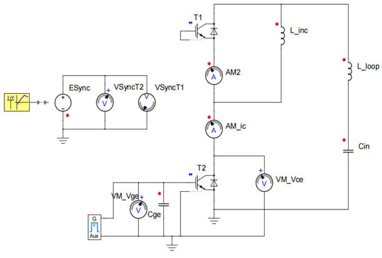
Figure 7.
DPT simulation model based on the behavior model of 4.5 kV/5 kA IGBT.
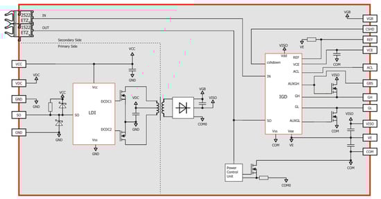
Figure 8.
The basic block diagram of the gate driver used for the IGBTs [25].
As shown in Figure 9a, Figure 10a, and Figure 11a, simulation results are quite close to the measured data overall. The sensors used for measurement are briefly introduced. A Rogowski coil is used for current measurement, and the bandwidth is up to 13 MHz. The range is up to 30 kA. The bandwidth for the oscilloscope used is from 200 MHz to 1 GHz. The bandwidth of the differential voltage probe used is 200 MHz, and the range is up to 30 kV. By zooming in on results during the turn-on and turn-off period of Vge, waveforms of the simulation and measured data, as shown in Figure 9b,c, are quite close but with minor differences. The simulated Vge starts falling about 2 μs earlier than the measured data. For the current Ic shown in Figure 10c, the simulated Ic starts falling about 2 μs earlier than the measured data during the turn-off period. The overshoot current of the simulated Ic is about 2000 A, larger than the measured data during the turn-on period shown in Figure 10b. For the current Ic, its rising time (from 10% to 90% Ic) is about 1.08 μs, and the di/dt is about 5.88 kA/μs (from 40% to 60% Ic). As depicted in Figure 11c, the simulated Vce during the turn-off period is about 1000 V larger than the measured data. This is caused by the clamped overshoot voltage Vce while no voltage clamping measures are taken for the simulation. For voltage, Vce, shown in Figure 11b, the two curves agree well overall, and the falling time of the simulated Vce is faster. For Vce illustrated in Figure 11c, the rising speed of the measured data is faster, and the time of the simulated Vce starting to rise is about 5 μs later than the measured data. The rising speed of Vce in Figure 11c is faster than its falling speed in Figure 11b, and the dv/dt is 1.83 kV/μs (from 40~60% Vce).
There are several reasons causing these mismatches between the simulation results and the measurement data. The first reason is that the behavior model is constructed based on the data obtained from the datasheet. These data cannot fully reflect the dynamic characteristics of the IGBT and diode devices. Especially, the accumulated charge in the base region of the diode cannot be modeled. This may cause the inaccuracy for the current overshoot as shown in Figure 10b. As for the current ring, it is caused by the parasitic parameters introduced by the IGBT packages, the main circuit, and the gate driver circuit, as well as cables used in the experiment. For Vce at Figure 11c, the rising speed of the measurement curve is faster than the simulated data. It is because the equivalent inductance in the test circuit is larger than that of the simulated circuit. Other factors, such as the carrier dynamics and electrothermal coupling effects of IGBTs and diodes, the temperature effect on this behavior model, as well as manufacturing dispersion, may also have an impact on the measurement.

Figure 9.
Comparison of simulation results and the measured data of current Vge during the turn-on period (b), the turn-off period (c), and the whole double pulse period (a).

Figure 10.
Comparison of simulation results and the measured data of current Ic during the turn-on period (b), the turn-off period (c), and the whole double pulse period (a).

Figure 11.
Comparison of simulation results and the measured data of current Vce during the turn-on period (b), the turn-off period (c), and the whole double pulse period (a).
4. Near-Field Simulation and Validation
From the DPT measured data, values of di/dt and dv/dt are quite large. By the IGBT behavior model, its dynamic characteristics are simulated and verified. The secondary equipment is vulnerable and might be affected by the radiated EM field generated by the di/dt and dv/dt. For the radiated EM field, the near-field is generally considered to have a strong influence on the secondary devices. In this section, the near-field around the IGBT’s gate driver PCB is simulated and validated.
Traditionally, square waveforms or trapezoidal waveforms can be used to approximate the current waveforms of Ic. However, some significant information is lost, and the inaccuracy of the high-frequency characteristics may be caused by this. Therefore, an S-shape waveform model is adopted to approximate current Ic, and it is also used to estimate the spectral envelope. A typical periodic S-shape waveform, which contains more information than the typical square waveforms and trapezoidal waveforms, is shown in Figure 12, and the Fourier coefficients of this waveform can be computed based on the periodic impulse train and differentiation properties of the Fourier series. The 1st, 2nd, and 3rd derivative waveforms of a periodic S-shape waveform are illustrated in Figure 12. The Fourier coefficients of this periodic S-shape waveform are calculated and expressed by (15) and (16) [26].
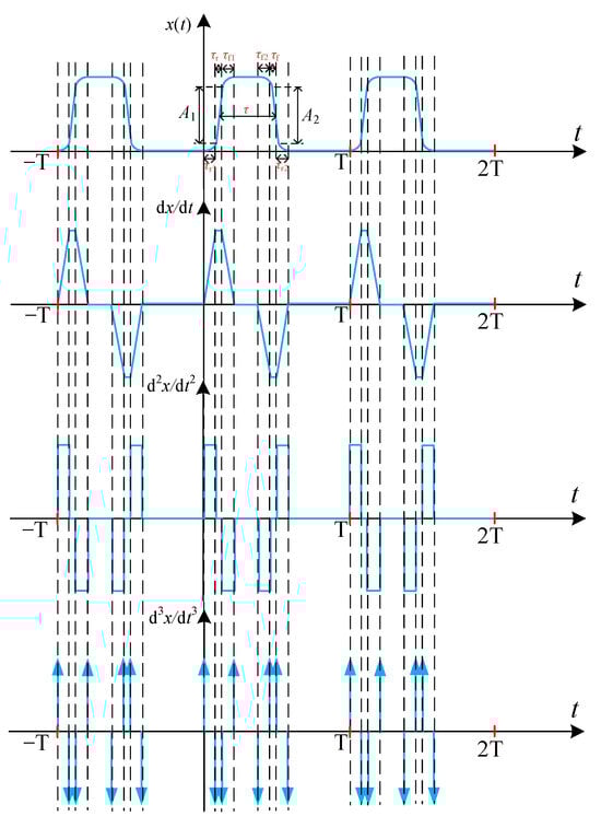
Figure 12.
Periodic S-shape waveform and its 1st, 2nd, and 3rd derivative waveforms.
Assuming that A1 = A2, τr = τf, τr1= τf1 = τr2 = τf2, then the Fourier coefficients of periodic S-shape waveforms can be expressed as,
Then, the three break points, fc1, fc2, and fc3, in the spectral envelope of a symmetrical periodic S-shape waveform shown in Figure 13 can be solved by,
Therefore, the breakpoints in the spectral envelope, fc1 = 10.6 kHz, fc2 = 159 kH, and fc3 = 1.27 MHz, are from the current waveform of Ic. When the distance to the EMI source is within λ/2π, it is usually considered to be a near field. Here, λ is the wavelength of the EM field. The wavelength of the 1.27 MHz EM field is about 236 m, and λ/2π is equal to 37.58 m. The distance between the gate driver PCB and the IGBTs is about 0.5 m, which is far smaller than λ/2π. Hence, the displacement current can be neglected in the region where the gate driver PCB and the IGBTs are located. In general, the near field can be approximated by an induction EM field when the distance to the EMI source is less than λ/20 = 1.88 m. Moreover, the magnetic field dominates within the near-field region since the EMI source has a larger current (10 kA) and a smaller voltage (3200 V).
The current generated by the double pulse test is similar to an S-shaped waveform. Hence, a transient magnetic field is induced. The rising and falling time is much smaller compared to the pulse width, which implies that the eddy current field would occur. Therefore, a 3D eddy current field is adopted to approximate this near-field. The governing equations for solving the magnetic field are given below.
Non-conductor region:
Conductor region:
Boundary condition:

Figure 13.
The spectral envelope of a symmetric periodic S-shape waveform.
A backward Euler solver is used to solve this time-dependent problem. A variable time-step is adopted; the minimum time-step is 0.4 us, while the maximum time-step is 50 us. An adaptive mesh method is adopted. The domain size surrounded for simulation is about 5 times larger than the MMC submodule. By using this method, the mesh can be automatically refined according to the error obtained during iteration for the simulation. The stop criterion is that the nonlinear residual is 0.005. The mesh and boundary condition parameters are listed in Table 2. The materials used are given in Table 3. The brief flowchart diagram is given in Figure 14. Firstly, we obtain the data, such as the transfer characteristics, from the datasheet of the IGBTs. A dynamic behavior model of the IGBT is built with the help of these data. Based on this dynamic model, a DPT circuit is constructed to obtain the current Ic, which is used as the excitation for near-field simulation. Lastly, the near field is calculated based on the quasi-static Maxwell equations.
Table 2.
Mesh/boundary parameters for simulation.
Table 3.
Material properties for simulation.
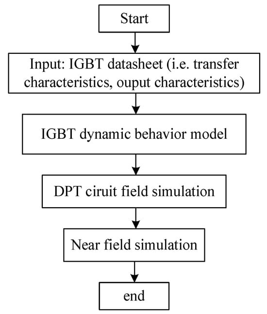
Figure 14.
The flowchart diagram of the near field proposed for simulation.
By the field-circuit coupling method, the current density, Js, can be obtained by the following formula listed below.
where I is the current through the conductor, and Δ is the area of the conductor cross-section.
After the determination of Js, the magnetic field can be simulated. The 3D geometry model of an MMC submodule is given in Figure 15a, and the schematic diagram of the magnetic field strength measurement setup is given in Figure 15b. Because of the complexity of the 3D geometry, only the relevant current path conductors are given in Figure 15a to depict how the current Ic flows in and out. As depicted in Figure 15a, the current path of Ic is Cin_p → HT1 → inductor → busbar → HT2 → T2 → HT3 → Cin_n. Here, Cin_p and Cin_n are the positive and negative of capacitors. HT1~HT3 are the heat sinks. IGBT T1 is shorted by an inductor. The inductor is not modeled in this 3D geometry model.
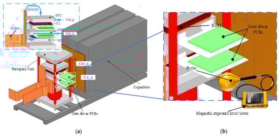
Figure 15.
Three-dimensional geometry model (a) and the measurement schematic diagram (b) of the MMC submodule.
The magnetic field simulated near the PCB of the gate driver is illustrated in Figure 16. The dominant component of the magnetic field strength for the upper gate driver PCB is parallel with its horizontal direction, while the lower PCB is parallel with its vertical direction, as shown in Figure 16a. The magnetic field strength of the surface for the magnetic exposure level tester during the measurement process is also shown in Figure 16b. To validate the effectiveness of the proposed method, a broadband EM field measurement device, namely the magnetic exposure level tester, is utilized to measure the magnetic field of the testing spot near the PCB shown in Figure 17a. The measured data is transferred to the oscillator by a BNC cable. A comparison between the simulation result and the measured data is illustrated in Figure 17b. The simulated result agrees with the measurement data roughly during the period when the current Ic is under excitation, as marked in Figure 17b–d. A typical waveform of Ic is illustrated in Figure 6b. The magnetic field strength, H, induced by Ic, which is marked by a rectangular box in Figure 17b. The magnetic field strength for these two parts agrees with the measured data roughly. There are some discrepancies between them. The reason for this discrepancy is that data noise is brought in during the measurement process, caused by the BNC cable. Though data noise appeared, the simulated data matched the measured data in tendency. As for the result, apart from these rectangular boxes shown in Figure 17b, the simulated data do not match the measured data. It is because the measured magnetic field strength is generated by the current IL, which is not considered since we cannot accurately build its current loop. The simulated magnetic field is generated by current Ic. It is the reason why these parts do not agree with each other during this period. In order to verify the proposed model, the magnetic field at another 2 positions is measured. The simulation result and the measured data are compared as shown in Figure 17c,d. Similarly to the result given in Figure 17b, the magnetic field strength at these 2 positions agrees with the measured data roughly. The reason for the discrepancy is explained above. The relative error is given in Figure 18. The maximum relative error of the magnetic field induced by the current Ic, which is the current source for the model simulated, is about 11%. The result with a large discrepancy is caused by the current IL, which is not modeled in this simulation. The numerical metrics about this simulation in the time window of Ic workers are also summarized in Table 4. The mean absolute error is 1.65, while the root mean square error is 16.90. The time shift between measured and simulated signals is about 50 us. It is clear that our model is validated when Ic dominates.
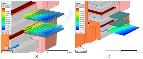
Figure 16.
Magnetic field strength of gate driver PCB (a) and magnetic exposure level tester surface (b) at 70.258 μs.
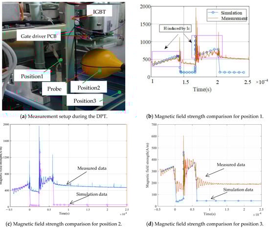
Figure 17.
Magnetic field strength comparison at different positions.
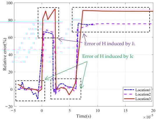
Figure 18.
The relative error of magnetic field strength, H, at different locations.
Table 4.
Numerical metrics.
5. Conclusions
The near field of a 4.5 kV/5 kA IGBT-based press-pack MMC-HVDC submodule with the maximum rated value of the DC collector current up to 5 kA is studied. For such a new device, its operating condition, such as the current handled, is different compared to other types of IGBTs. The di/dt and the EMI caused by it for such an IGBT need to be studied since it is quite important and expensive for MMC-HVDC submodules and valve stations. The gate driver suffering from the IGBT turn-on/off period is susceptible to the EMI since the distance between them is quite close. It is urgent to solve the near-field of gate drivers suffering from the IGBTs near them, and it is practical for the design of the MMC submodule in the case of the arrangement of IGBT gate driver PCBs.
Since the computation cost of the near field solved by the full-wave Maxwell equations is high for a complex 3D geometry model, a simulation method is proposed for the near-field calculation of 4.5 kV/5 kA IGBT-based MMC submodules under dual pulse test. This method integrates the IGBT dynamic switching behavior and the quasi-static Maxwell equations for near-field simulation since the distance between the EMI source and susceptible subject is much smaller than the electromagnetic wavelength. By using this method, we can solve the near-field more cost-effectively with desirable accuracy.
In a word, the novelty and contribution of this paper can be attributed to (1) the near field of a 4.5 kV/5 kA IGBT-based press-pack MMC submodule with the turning-off current up to 10 kA is conducted, which is rarely studied, and (2) an integration method that combines a dynamic behavior model and a quasi-static Maxwell model helps to fasten the calculation speed of the near field with desirable accuracy.
This proposed model can predict the near field caused by the current Ic during the DPT in distances smaller than λ/2π. This means that the transient period cannot be too fast. Because of cables connecting with the inductance, the magnetic field strength will be affected by its current when the IGBT is in the turn-off state. This is the biggest error source between the simulation result and the measured data during these periods. This error source can be fixed by a more comprehensive model, which includes cables connecting the inductance. The proposed model provides a tool to understand the EMI mechanism and its effect on the secondary devices with a desirable accuracy as well as an acceptable cost, and it is helpful for the arrangement of IGBT gate driver PCBs in the design stage.
The next step is to study a more comprehensive model, including the IL loop to eliminate this error, how the secondary devices, such as the driver PCBs, suffer from the magnetic field generated by the IGBT during the turn-on/off period, and methods to suppress the EMI.
Author Contributions
Conceptualization, H.L. and S.W.; methodology, H.L. and Z.C.; validation, Y.H. (Yongjie Hu) and K.X.; formal analysis, Y.H. (Yongrui Huang); data curation, K.X.; writing—original draft preparation, X.Z. and L.L.; writing—review and editing, Z.S. and K.L.; visualization, H.L.; project administration, H.L.; funding acquisition, H.L. All authors have read and agreed to the published version of the manuscript.
Funding
This work was supported by the Key Research and Development Projects in Henan Province (252102240120).
Data Availability Statement
The authors declare that the data supporting the findings of this study are available within the paper.
Conflicts of Interest
Author Hailin Li, Zhilei Si, Lulu Liu, Yongjie Hu, Kun Liu, Zhongting Chang, Yongrui Huang, Kepeng Xia, Xiaofeng Zhou were employed by the company XJ Electric Corporation, LTD. The remaining authors declare that the research was conducted in the absence of any commercial or financial relationships that could be construed as a potential conflict of interest.
Abbreviations
The following abbreviations are used in this manuscript:
| MMC | Modular Multilevel Converter |
| IGBTs | Insulated gate bipolar transistors |
| HVDC | High Voltage Direct Current |
| DPT | Double Pulse Testing |
| PCB | Printed Circuit Board |
| EMI | Electromagnetic Interference |
| VSC | Voltage Source Converter |
| CM | Common mode |
| IC | Integrator Chip |
| PWM | Pulse width modulation |
| DC | Direct Current |
| GPUs | Graphics Processing Units |
| ADE | Ambipolar diffusion equation |
| BJT | Bipolar junction transistor |
| MOSFET | Metal oxide semiconductor field effect transistor |
| EM | Electromagnetic |
| BNC | Bayonet Neill–Concelman |
| VGS | Gate-source voltage |
| VDS | Drain-source voltage |
| VP | Pinch-off voltage |
| AFET, MFET, NFET, K | Coefficients |
| VBE | Base-emitter voltage |
| Ic | The collector current |
| Isat_BJT, MBJT, BN | Parameters of the BJT |
| k | Boltzmann constant |
| q | The electron charge |
| Tjnc | The junction temperature |
| C0, α, β, δ and Vdiff | Coefficients for junction capacitances |
| Kshift | The parameter |
| VJCT | The p-n junction voltage |
| τ, M | Coefficients for the diffusion capacitance model within the freewheeling diode |
| Isat_fwd, Mfwd, and Rb_fwd | Parameters for the freewheeling diode |
| Vfwd | The freewheeling diode voltage |
| INOM | The nominal current of igbts |
| ks | The turn-off slope rate of the waveform |
| τfwd | The lifetime of carriers |
| Tn | The transit time of the electron |
| A | Vector magnetic potential |
| ν | Magnetic reluctivity |
| σ | Conductivity |
| φ | Electrical potential |
| Js | Current density |
References
- Perez, M.; Ceballos, S.; Konstantinou, G.; Pou, J.; Aguilera, R. Modular multilevel converters: Recent achievements and challenges. IEEE Open J. Ind. Electron. Soc. 2021, 2, 224–239. [Google Scholar] [CrossRef]
- Liu, Z.; Guo, X. High-voltage Large-capacity VSC Valve Reliability Enhancement. Power Syst. Technol. 2020, 44, 3604–3613. [Google Scholar]
- Liu, C.; Li, B.; Zhang, Y.; Jiang, Q.; Liu, T. The LCC type DC grids forming method and fault ride-through strategy based on fault current limiters. Int. J. Electr. Power Energy Syst. 2025, 170, 110843. [Google Scholar] [CrossRef]
- Wang, Z.; Li, H.; Chu, Z. A Review of EMI Research in Modular Multilevel Converter for HVDC Applications. IEEE Trans. Power Electron. 2022, 37, 14482–14498. [Google Scholar] [CrossRef]
- Sun, T.; Pei, X.; Shan, Y.; Pei, J.; Jiang, D. Submodule Switching-State Based EMI Modeling and Mixed-Mode EMI Phenomenon in MMC. IEEE Trans. Power Electron. 2023, 38, 1831–1843. [Google Scholar] [CrossRef]
- Zhang, B.; Wang, S. A Survey of EMI Research in Power Electronics Systems with Wide-Bandgap Semiconductor Devices. IEEE J. Emerg. Sel. Top. Power Electron. 2020, 8, 626–643. [Google Scholar] [CrossRef]
- Liu, B.; Ren, R.; Zhang, Z. Impacts of high frequency, high di/dt, dv/dt environment on sensing quality of GaN based converters and their mitigation. CPSS Trans. Power Electron. Appl. 2018, 3, 301–312. [Google Scholar] [CrossRef]
- Nguyen, V.S.; Kerachev, L.; Crebier, J.C. Characterization and analysis of an innovative gate driver and power supplies architecture for hf power devices with high dv/dt. IEEE Trans. Power Electron. 2017, 32, 6079–6090. [Google Scholar] [CrossRef]
- Chen, J.; Jiang, D.; Sun, W.; Shen, Z.; Zhang, Y. A family of spread-spectrum modulation schemes based on distribution characteristics to reduce conducted EMI for power electronics converters. IEEE Trans. Ind. Appl. 2020, 56, 5142–5157. [Google Scholar] [CrossRef]
- Shan, Y.; Pei, X.; Sun, T.; Zhang, M.; Zhou, P.; Jiang, D. Space spread-spectrum strategy for mmc to reduce the conducted EMI. IEEE Trans. Ind. Electron. 2022, 69, 10807–10818. [Google Scholar] [CrossRef]
- Sun, T.; Pei, X. Comparison analysis on EMI sources of MMC under NLM and CPS-PWM strategies. In Proceedings of the 2019 4th IEEE Workshop on the Electronic Grid, Xiamen, China, 11–14 November 2019. [Google Scholar]
- Wang, J.; Li, H.; Yang, Z. Common-mode voltage reduction of modular multilevel converter based on chaotic carrier phase shifted sinusoidal pulse width modulation. In Proceedings of the 2020 IEEE International Symposium on Electromagnetic Compatibility & Signal/Power Integrity, Reno, NV, USA, 28 July–28 August 2020. [Google Scholar]
- Li, H.; Wang, J.; Yang, Z. Common-mode voltage reduction of modular multilevel converter based on six-segment carrier level shifted sinusoidal pulse width modulation. In Proceedings of the 2020 IEEE 9th International Power Electronics and Motion Control Conference (IPEMC2020-ECCE Asia), Nanjing, China, 29 November–2 December 2020. [Google Scholar]
- Chen, J. Common-mode voltage reduction scheme for mmc with low switching frequency in ac-dc power conversion system. IEEE Trans. Ind. Inform. 2022, 18, 278–287. [Google Scholar] [CrossRef]
- Jin, M.; Weiming, M. Power Converter EMI Analysis Including IGBT Nonlinear Switching Transient Model. IEEE Trans. Ind. Electron. 2006, 53, 1577–1583. [Google Scholar] [CrossRef]
- Zhu, R.; Lin, N.; Dinavahi, V.; Liang, G. An accurate and fast method for conducted EMI modeling and simulation of MMC-Based hvdc converter station. IEEE Trans. Power Electron. 2020, 35, 4689–4702. [Google Scholar] [CrossRef]
- Zhang, J.; Lu, T.; Zhang, W.; Shen, H.; Yang, Z. Frequency-Time domain characteristics of radiated electric fields in a multi- terminal MMC-HVDC station. IEEE Access 2019, 7, 99937–99944. [Google Scholar] [CrossRef]
- Liang, G.; Zhu, R. Predictive analysis for radiated electromagnetic disturbance in MMC-HVDC valve hall. CPSS Trans. Power Electron. Appl. 2020, 5, 126–134. [Google Scholar] [CrossRef]
- Sun, H.; Du, L.; Liang, G. Calculation of electromagnetic radiation of VSC-HVdc converter system. IEEE Trans. Magn. 2016, 52, 9400504. [Google Scholar] [CrossRef]
- Wen, F.; Lu, Z.; Cao, J. Improvement of EMC capability of the submodule’s controller in the VSC-HVDC converter. J. Glob. Energy Interconnect. 2020, 3, 248–254. [Google Scholar]
- Wang, H. Research on Magnetic Disturbance Characteristics of Drive Control Unit of Flexible DC Converter Valve. Ph.D. Thesis, North China Electric Power University, Beijing, China, June 2021. [Google Scholar]
- Shim, H. Inverter modeling including non-ideal IGBT characteristics in Hybrid Electric Vehicle for accurate EMI noise prediction. In Proceedings of the 2015 IEEE International Symposium on Electromagnetic Compatibility, Dresden, Germany, 16–22 August 2015. [Google Scholar]
- Shim, H. Analysis of high frequency characteristics of power inverter using accurate IGBT model based on datasheet and measurement. In Proceedings of the 2015 IEEE Electrical Design of Advanced Packaging and Systems Symposium (EDAPS), Seoul, Republic of Korea, 14–16 December 2015. [Google Scholar]
- 5SMA3000L450300, ABB. Available online: https://new.abb.com/products/5SMA3000L450300/5sma3000l450300 (accessed on 1 October 2018).
- 1SC0450, Power Integration. Available online: https://www.hy-line-group.com/products/hpc/datasheet/powerintegrations/product_brief_1sc0450_2015.pdf (accessed on 1 January 2015).
- Zhang, B. EMI Modeling and Reduction of Conducted Noisein Switching Power Converters. Ph.D. Thesis, Kyushu University, Fukuoka, Japan, July 2019. [Google Scholar]
Disclaimer/Publisher’s Note: The statements, opinions and data contained in all publications are solely those of the individual author(s) and contributor(s) and not of MDPI and/or the editor(s). MDPI and/or the editor(s) disclaim responsibility for any injury to people or property resulting from any ideas, methods, instructions or products referred to in the content. |
© 2025 by the authors. Licensee MDPI, Basel, Switzerland. This article is an open access article distributed under the terms and conditions of the Creative Commons Attribution (CC BY) license.