Article

The Improvement of the Mathematical Model of a Calculable Voltage Standard with a Single Junction Thermal Voltage Converter


by
Michał Pecyna
*,
Krzysztof Kubiczek
and
Marian Kampik
*
Department of Measurement Science, Electronics and Control, Faculty of Electrical Engineering, Silesian University of Technology, 44-100 Gliwice, Poland
*
Authors to whom correspondence should be addressed.
Energies 2026, 19(1), 62; https://doi.org/10.3390/en19010062
Submission received: 5 November 2025 / Revised: 3 December 2025 / Accepted: 18 December 2025 / Published: 22 December 2025
(This article belongs to the Special Issue Stationary Energy Storage Systems for Renewable Energies)

Abstract

This paper presents the modification and experimental validation of a mathematical model for a single junction thermal voltage converter (SJTC) designed for high-precision alternating current (AC) voltage transfer. The original model is severely constrained by two main issues: (1) computational instability above 50 MHz due to the limitations of the housing impedance approximation, and (2) insufficient accuracy above 1 MHz due to the neglect of high-frequency skin effect and magnetic core effects in the Dumet wire leads. Significant refinements are subsequently implemented to extend the calculable frequency range of the standard from 1 to 100 MHz. This required re-evaluation of the Dumet wire leads’ frequency-dependent resistance and inductance using finite element method (FEM) simulations, which accounted for the skin effect and the magnetic permeability of the FeNi42 core. Additionally, the housing impedance calculation is stabilized using a formulation based on scaled modified Bessel functions, and the electrical conductivity of the input N-type connector pin is explicitly modeled. The improved model is validated against a reference calorimetric thermal voltage converter (CTVC) using 3 and 5 V nominal voltage standards. The results indicated excellent agreement between the calculated and measured AC-direct current (DC) transfer differences up to 10 MHz. In the extended frequency regime, the model correctly predicted the transition to negative transfer differences observed above 2 MHz for the 5 V standard. The largest discrepancies between the measured and calculated values occurred at 100 MHz. The measured transfer difference reached −15,090 (µV/V) with an expanded uncertainty (k = 2) of 190 (µV/V), whereas the calculated value is −12,500 (µV/V) with an expanded uncertainty of 3900 (µV/V). Although the deviation between the model and measurement increased above 30 MHz, the results remained consistent within the expanded measurement uncertainties across the entire 10 kHz to 100 MHz range, demonstrating the model’s suitability for providing traceability in high-frequency voltage metrology.

1. Introduction

Accurate measurement of the root mean square (RMS) value of alternating current (AC) voltage is important in the field of electrical metrology, essential for ensuring traceability in calibration laboratories, verifying the performance of measurement instruments, and supporting applications in telecommunications and high-frequency electronics [1]. Among the available measurement techniques, the AC–direct current (DC) transfer method using thermal voltage converters (TVC) is widely recognized for its ability to achieve the highest accuracy across a broad frequency range [1,2]. In simple terms, this method determines the RMS value of an AC signal by comparing it to a DC voltage that produces the same heating effect in the heater of the TVC [1,2].
In the 1–100 MHz frequency range, the AC-DC transfer difference of the TVC is caused by physical effects such as the skin effect, impedance mismatches [3], electromagnetic wave phenomena, and thermoelectric effects [4]. The magnitude of the AC-DC transfer difference and its uncertainty strongly depend on the signal frequency [1,5].
Among TVCs, one of the recent single-junction thermal voltage converters (SJTCs) designs was developed by Grzenik and Kampik [4]. The modifications of the early design included the application of a range resistor made of a segment of resistive wire and the replacement of the GR-874 connector with an N-type connector at the converter’s input. Planar multijunction thermal voltage converters (PMJTCs), the second TVC type, feature a thin-film planar design with a resistor (heater) deposited on an insulating substrate such as Al2O3, AlN or, more recently, diamond [6]. This configuration provides higher sensitivity compared with SJTCs and ensures better fabrication repeatability. In recent years, research on PMJTCs has been focused mainly on improving the long-term stability of the thin-film thermoelements by eliminating Bi–Cu junctions, which are prone to degradation [7,8,9]. This improvement was confirmed by long-term stability tests [8], accelerated aging tests [7], and highly accelerated life testing (HALT) [9]. Other studies addressed the optimization of the thermocouple geometry for the maximization of the signal-to-noise ratio (SNR) [10]. Further developments have aimed at minimizing the AC–DC transfer difference in a 10 kHz–1 MHz frequency band, e.g., by employing a U-shaped heater sputter-deposited on an AlN chip [11]. A new research direction involves the use of diamond substrate characterized by extremely high thermal conductivity, enabling the reduction in the thermal time constant and the achievement of a more uniform temperature distribution compared with PMJTCs using Al2O3 and AlN substrates [6].
Calorimetric thermal voltage converters (CTVCs), the third type of TVCs, are characterized by a coaxial structure, where the resistor (heater) is located at the end of the inner center conductor of the coaxial line, terminated by a thin copper disk. A multijunction thermoelectric sensor measures the temperature difference between this copper disk (thermally connected to the heater) and the approximately ambient reference temperature of the CTVC enclosure. This configuration provides improved impedance matching, which extends the operational frequency range and minimizes the AC-DC transfer difference. The first CTVC was developed at the National Research Council of Canada (NRC) by Filipski et al. [1,12]. The design was later refined by the Silesian University of Technology (SUT) [13]. The modifications included the implementation of a thermoelement fabricated using flex-printed circuit board (PCB) technology, which enhanced the converter sensitivity and improved manufacturing repeatability with respect to the original design. Additionally, the use of a coaxial line made of non-magnetic stainless steel (type 304), providing electrothermal symmetry between the central conductor and hollow cylinder, contributed to minimizing the reversal error by about 90% [14]. The authors demonstrated that replacing the currently used microwave rod resistor with a disk-type resistor, although improving temperature uniformity and simplifying the mechanical structure, significantly increases the AC-DC transfer difference above 10 MHz [13].
SJTC-type standards are characterized by relatively low AC-DC transfer difference values and good long-term stability. Their simple construction (e.g., without the need for expensive thin-film vacuum technology) makes them a more economical alternative to PMJTC-type standards. Moreover, the coaxial geometry of SJTCs simplifies their mathematical model, which is particularly important for their application as calculable standards.
Several mathematical models have been proposed to predict the transfer difference of various designs of SJTC-type TVCs [4,15]. One of them is the model developed at SUT [4]. The model is accurate up to about 1 MHz. However, above this frequency, its performance is deteriorated by two important factors: (i) the material properties of some of the parts used to assemble the device, which were unknown during its development, and (ii) the model becomes numerically unstable at a high frequency range.
The previously developed mathematical model of the presented SJTC-type standards exhibits several limitations that hinder their applicability at higher frequencies. One of them is due to the ferromagnetic property of SJTC glass-through leads made from an alloy called Dumet [4]. Dumet is a wire consisting of a core made of FeNi42 alloy covered with a copper coating. It is characterized by a coefficient of thermal expansion close to that of glass, which makes it suitable for applications requiring the maintenance of hermeticity in glass-to-metal seals, such as in the manufacturing of light bulbs. The frequency characteristics of the Dumet leads were previously determined under the assumption of a constant magnetic permeability of the wire core, which represents an oversimplification within the frequency range up to 100 MHz. In addition, the earlier expressions describing the housing impedance can cause numerical stability issues, particularly in computations performed at higher frequencies. Furthermore, in the previous mathematical model, the electrical parameters of the N-type connector pin were adopted in a simplified form, without directly accounting for its actual geometry and material composition, which—to a certain extent—may affect the reliability of the AC–DC transfer difference computations at high frequencies.
This work addresses these limitations by developing an improved mathematical model of an SJTC-type TVC that extends its frequency range from 1 to 100 MHz. These improvements include several steps: first, the frequency-dependent properties of the Dumet wire are re-evaluated using finite element method (FEM) simulations in COMSOL Multiphysics version 6.3 software [16]. Next, the currently existing mathematical expression describing the housing impedance is modified to ensure better numerical stability and improved accuracy in the calculations. Finally, the electrical conductivity of the N-type connector central pin and a solder joint is estimated based on their geometry and material composition.
The model is implemented in MATLAB version R2023b software [17] to enable fast and stable matrix numerical computation, including efficient estimations of uncertainty using the Monte Carlo method, and optimization of the constructions of further SJTC-type TVCs. The proposed new model is validated by measuring the AC-DC transfer difference of the physical model of the TVC of nominal voltage of 5 V [18] using the CTVC developed at SUT as a reference [19]. The article is structured as follows: Section 2 describes the fundamentals of SJTC-type thermal converters, including the definition of the AC–DC transfer difference and a description of the standard developed at SUT. Section 3 outlines the previously developed mathematical model of the SJTC standard designed at SUT [4], including its theoretical basis and uncertainty evaluation using the Monte Carlo method. Section 4 discusses the modifications introduced in the improved model, such as FEM-based re-evaluation of Dumet wire frequency-dependent parameters, the reformulation of the housing impedance, and the determination of the N-type connector pin conductivity. Section 5 presents the results obtained from the improved model and their comparison with experimental data [18]. Section 6 provides conclusions and outlines future research directions.

2. SJTC State of the Art

2.1. AC-DC Transfer Difference

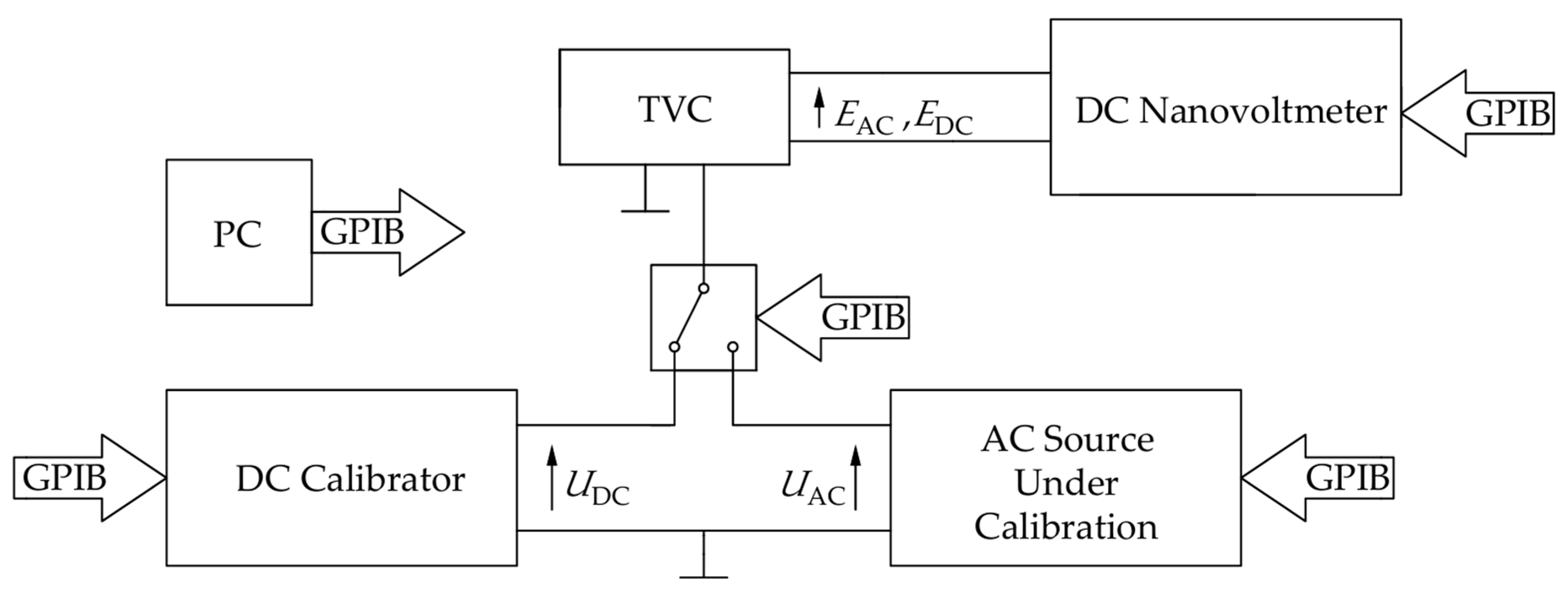
A schematic representation of the simplified AC–DC transfer difference measurement setup that illustrates the principle of operation is depicted in Figure 1.
The definition of AC RMS voltage originates from the Joule-Lentz heating principle: it is equal to the equivalent DC voltage that, when applied across the same resistance for the same amount of time, dissipates the same amount of thermal energy.
Thus, to simplify, a TVC is composed of a resistor (heater) and a thermocouple used to measure the temperature rise above the ambient temperature. In the first step, an unknown AC voltage is applied to the TVC’s input, while a DC nanovoltmeter measures the steady-state output voltage, which is proportional to the temperature rise of the heater. Subsequently, a known value of the DC voltage from a precision calibrator is applied to the TVC heater and is adjusted until the output voltage is the same as the one previously obtained for the AC case. If the output voltages are the same, the unknown AC RMS voltage should be equal to the newly found DC voltage equivalent. However, at higher frequencies, some phenomena occur that are absent for DC; for example, the skin effect, standing waves, reflections, interferences, and effects due to impedance mismatch. All these combined create the so-called AC-DC transfer difference, which is one of the most relevant parameters of TVCs. It is mathematically defined as follows [5]:
δ U = U AC U DC U DC |   E AC = E DC ,
where U AC is the RMS value of the AC voltage, U DC is a value of standard DC voltage, and E AC and E DC are the values of the TVC output voltage for the applied voltages U AC and U DC , respectively.

2.2. SJTC Developed at SUT

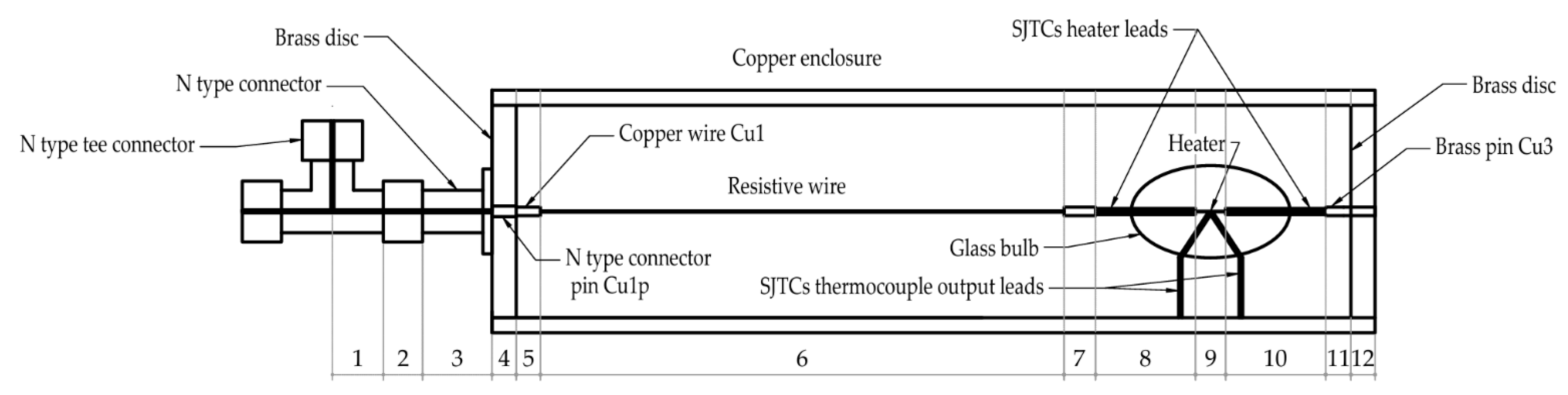
The SJTC-based calculable TVC, developed at SUT in 2014 [4], is equipped with an N-type connector and a range resistor made of ISAOHM resistance wire. A significant modification was the replacement of the expensive SJTC with Pt–Ir alloy leads with an SJTC with Dumet wires. The cross-sectional diagram of the SUT TVC is presented in Figure 2.
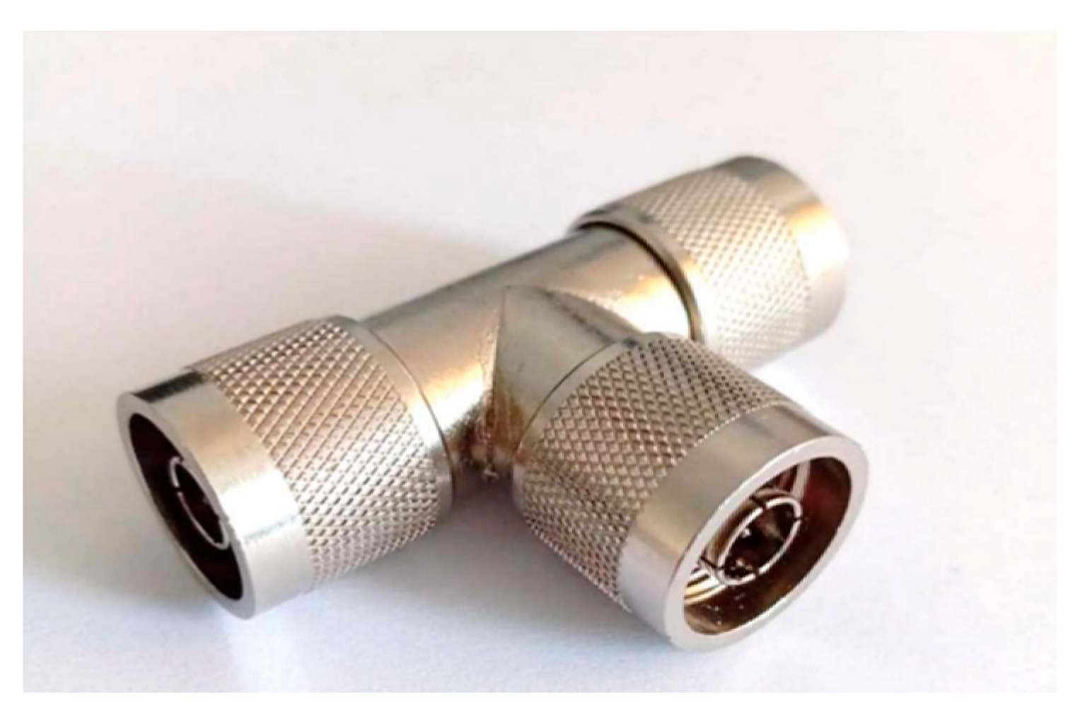
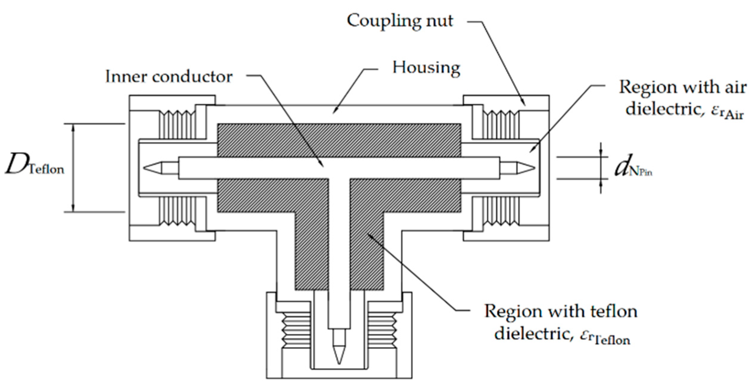
The model was divided into 11 sections. Figure 3 shows the N-type tee connector employed in the design.
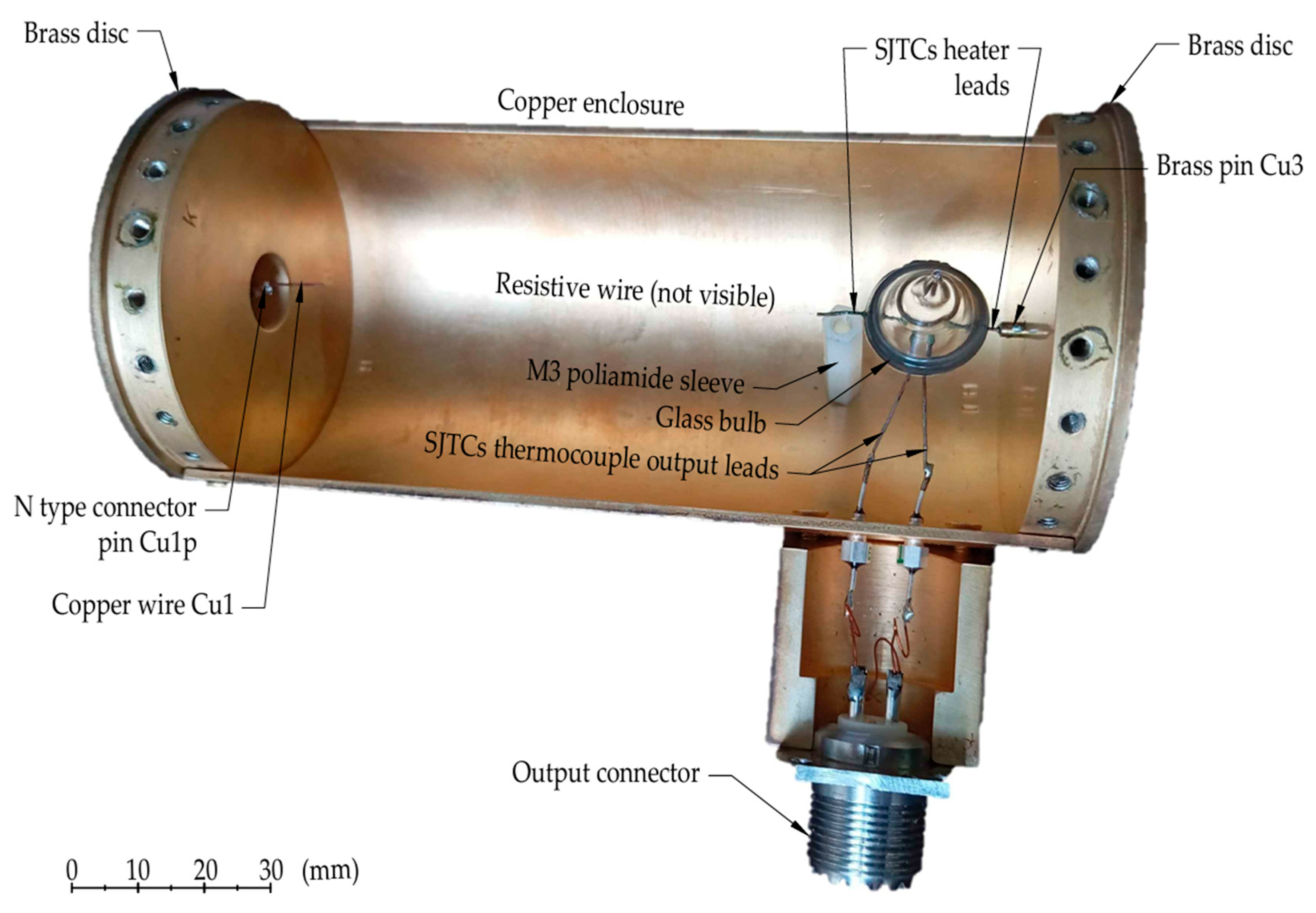
The first section of the SJTC, depicted in Figure 2, is a tee (Figure 3) connected to the input N-type connector (sections 2–4) of the TVC. It corresponds to the area between the internal wire’s connection point and the reference plane of the N-type connector. In an N-type coaxial connector, the reference plane is defined as the mating surface of the outer conductors of the male and female parts. The position of the reference plane is specified in the standard [20]. The tee is equipped with three female N-type sockets and is designed for a characteristic impedance of 50 Ω. The N-type connector (sections 2–4) is terminated with a male socket on the tee side and a brass pin (Cu1p). Both the tee and the N-type connector have sectors where the insulator is air and sectors with a Teflon (PTFE) insulator. The front closing disc has holes for attaching the N-type connector base and inserting the Cu1p pin into the housing. A copper Cu1 wire (section 5) is soldered to the brass Cu1p pin (section 4). The range resistor (section 6), made of ISAOHM wire, determines the rated voltage of the standard. A wire with a diameter of 25 µm was used for UN = 3 V, while a 15-µm wire was utilized for UN = 5 V. The wire was connected to the Cu1 and Cu2 (section 7) wires by welding. The next wires (Cu2 and Cu3, defined in section 10) were soldered to the SJTC heater leads (sections 8 and 10), made of Dumet. Soldering was performed with Sn60Pb40 solder (Cynel-Unipress, Warsaw, Poland). The SJTC heater (section 9) is made of non-magnetic EVANOHM wire [21]. A single thermoelectric junction mounted on the heater converts the temperature difference between the contact point and the terminals into the SJTC’s output voltage. The SJTC output terminals and heater leads were made of Dumet. The Cu3 wire (section 11) (made of brass, despite its designation) was threaded on one end and screwed into the rear closing disc. The internal design of a similar TVC with a lower nominal input voltage (UN = 1.5 V), following a partial disassembly of the housing, is illustrated in Figure 4.
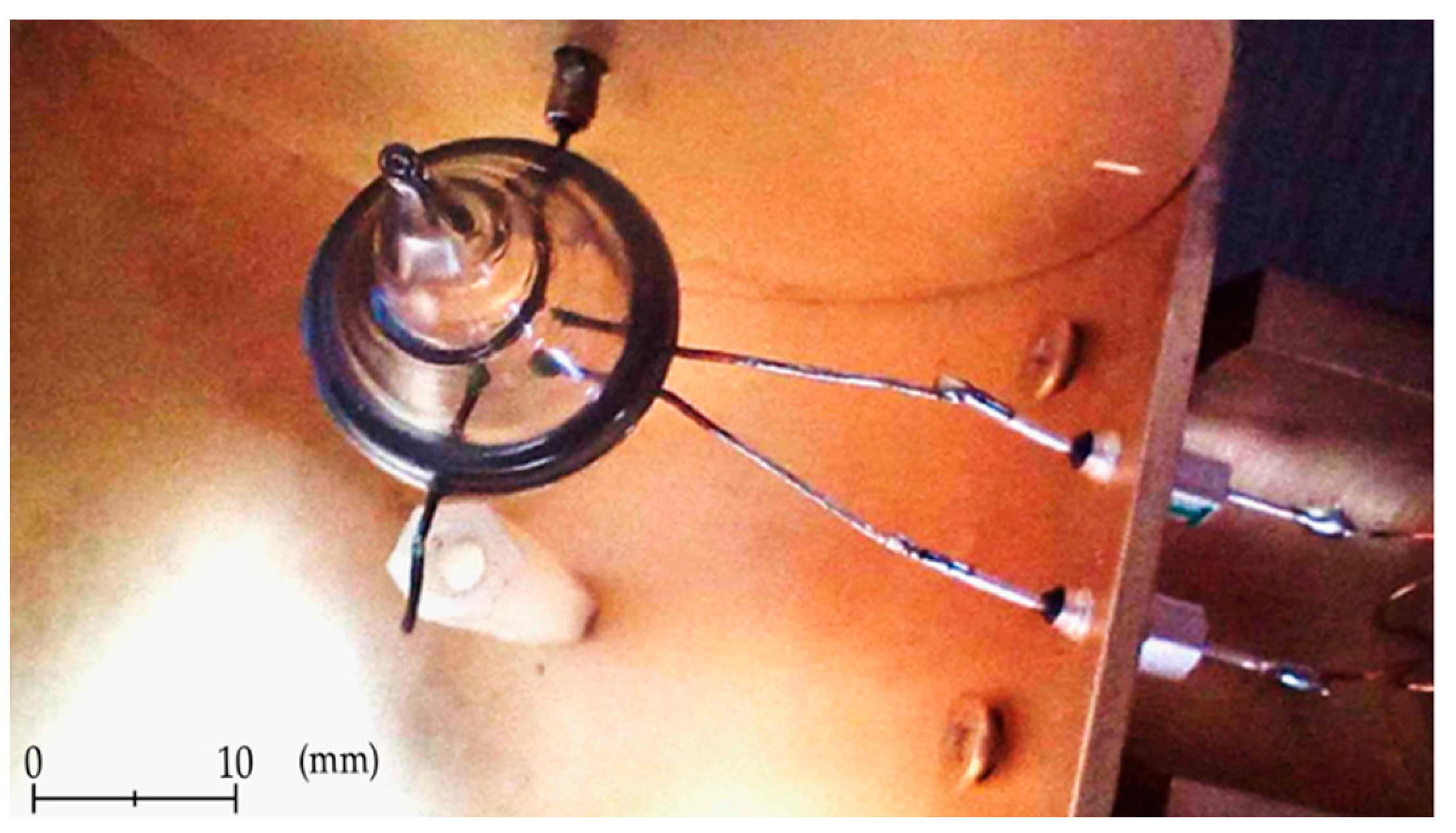
In the case of the 1.5 V standard, one of the SJTC’s heater leads was used instead of the Cu2 wire, which is why this element is not marked in Figure 4. The threaded holes visible in the closing disc are designed to receive the screws that fasten the half of the housing cover made from brass. The hole arrangement supports a uniform current distribution, thereby reducing the transfer difference and simplifying the mathematical model. The output connector of the TVC is not included in the cross-sectional diagram in Figure 2 because it does not appear in the mathematical model of the standard. Figure 5 shows details of the SJTC mounting.
Section 8 contains an M3 polyamide threaded sleeve, which supports the SJTC. This support is necessary due to the very small diameter of the resistive wire, which cannot withstand mechanical loads. The housing is made of phosphorus-deoxidized copper (DHP) and closed on both sides with MO58 brass discs (sections 4 and 12). The housing was coated with a thin gold layer to provide protection against environmental factors.

3. Mathematical Model

3.1. Mathematical Model of AC-DC Transfer Difference

The mathematical model given in ref. [4] allows for numerical determination of the transfer difference δ U in the frequency range from 10 kHz to 1 MHz. The calculations are based on a relation similar to Equation (1) but expressed in its transformed form, i.e., [4]
δ U = U AC U DC U DC P AC = P DC ,
where P AC denotes the Joule power dissipated in the SJTC’s heater when voltage U AC is applied to its terminals, and P DC denotes the Joule power dissipated in the SJTC’s heater when voltage U DC is applied to its terminals.
Equation (2) follows directly from the definition of the AC-DC transfer difference, under the assumption that thermoelectric effects have no significant influence on δ U . Such an assumption is acceptable because their contribution in the 10 kHz–1 MHz frequency range is negligibly small. The model was implemented in the Wolfram Mathematica environment. For modeling purposes, the following assumptions were adopted:
  • Coaxial symmetry for each model region;
  • Homogeneity of the materials used in the construction;
  • Each model region may be analyzed independently.
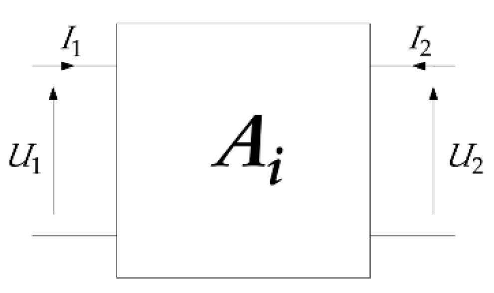
Each of the sections shown in Figure 2 can be treated as a two-port network and described by a matrix. The schematic representation of an elementary ABCD matrix is shown in Figure 6.
The two-ports representing the ith individual region of the standard are described by the following matrix equation [4]:
U 1 I 1 = A i U 2 I 1 = A i B i C i D i U 2 I 2 .
The definitions of the voltages and currents are shown in Figure 6. The matrix A y , describing the entire standard, is the product of the matrices A i , which corresponds to the individual regions of the model [4]:
A y = 1 12 A i .
Such a structure of the model enables independent description and analysis of each region.

3.2. Mathematical Models of Individual Sections

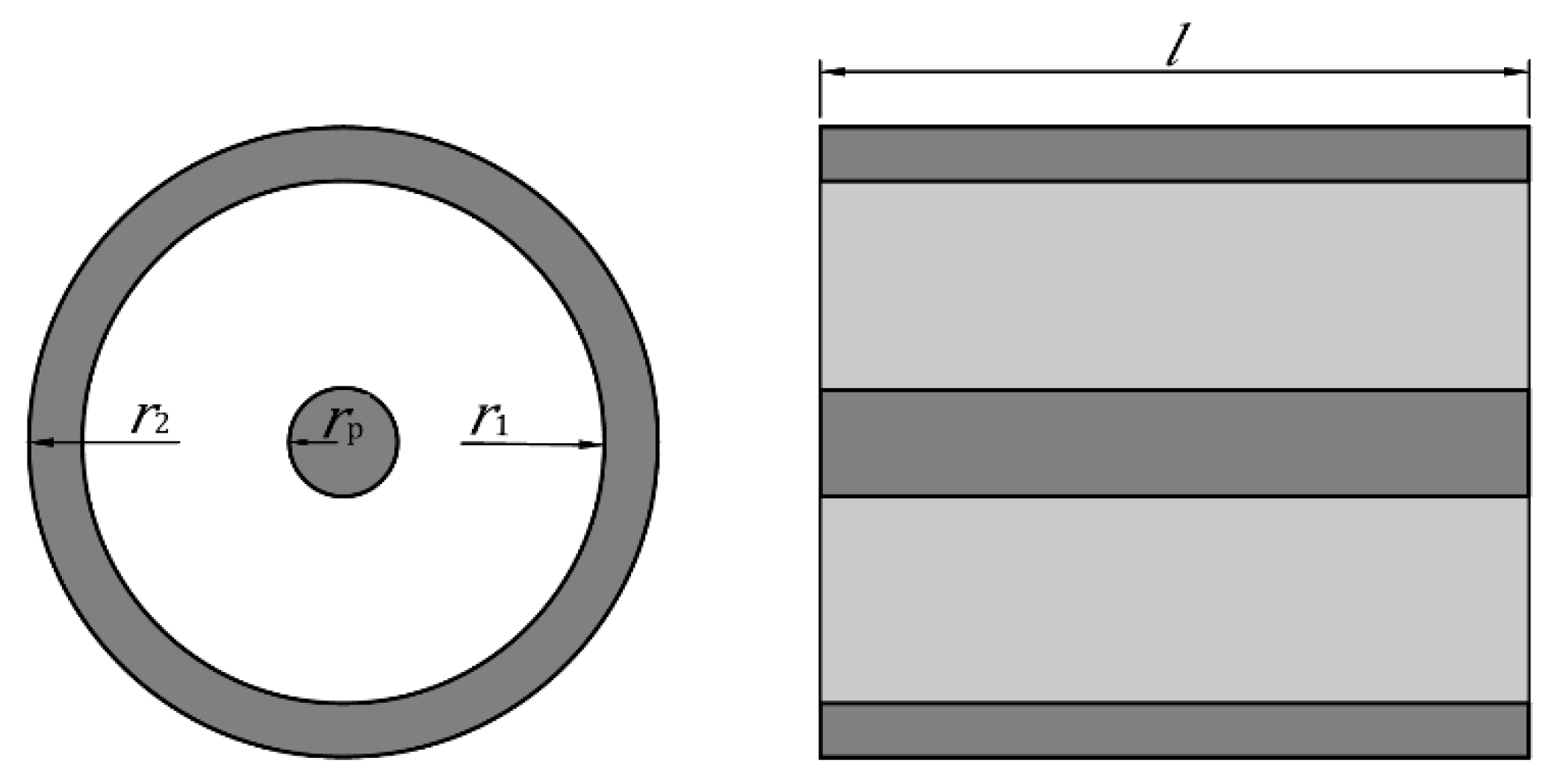
Figure 7 displays the schematic diagram of a single coaxial section of the model, combined with its geometric dimensions’ definitions.
The geometric dimensions, indicated in Figure 7 (i.e., r1, r2, rp, and l), denote the inner and outer radii of the housing, the radius of the inner conductor, and the length of the considered model region, respectively. The transmission matrix of this region, derived from telegrapher’s equations, has the form [22]:
A i = cosh γ l Z C sinh γ l 1 Z C sinh γ l cosh γ l ,
where Z c is the characteristic impedance of the long line and γ is the propagation constant:
Z C = j ω L + R j ω C ,
γ = j ω C ( j ω L + R ) .
The impedance of the closing discs of the housing, Z Disc , was modeled via the relation [15]:
Z Disc = 1 + j 2 π π f μ r Disc μ 0 σ Disc ln r 2 r 1 coth l 1 + j π f μ r Disc μ 0 σ Disc ,
where σ Disc is the electrical conductivity and μ r Disc is the relative magnetic permeability of the closing disc material.
To avoid inconsistencies resulting from the use of different formulae, the DC resistance of the closing discs R Disc was evaluated from Equation (8) for a frequency of 1 Hz, where the influence of the skin effect can be neglected. The DC resistance of the inner conductor R i and of the housing R o is computed from geometric dimensions and the electric conductivity of these components for each analyzed section of the model.
The impedance of the inner conductor Z i was determined using the relation [4]:
Z i = l j ω μ 0 μ i σ i π r i σ i I 0 r i j ω μ 0 μ i σ i I 0 r i j ω μ 0 μ i σ i ,
where I 0 ( ) and I 0 ( ) denote the modified Bessel functions of the first kind of order zero and its derivative, respectively. Equation (9) is not used for computing SJTC’s heater leads impedance due to the ferromagnetic properties of the Dumet wire. Evaluation of the SJTC’s heater leads impedance is presented in Section 4.2. The impedance of the housing can be defined by the expression [23]:
Z o = ml r 1 σ o π I 0 m r 1 K 0 m r 2 K 0 m r 1 I 0 m r 2 I 0 m r 1 K 0 m r 2 K 0 m r 1 I 0 m r 2 ,
where K 0 ( ) and K 0 ( ) denote the modified Bessel function of the second kind of order zero, and its derivative, and the propagation constant m is defined here as follows:
m = j σ o μ 0 μ o ω .
The modified Bessel functions in Equation (10) change value steeply with their arguments, leading to numerical instability at high frequencies and for large enclosure radii. To avoid this instability, the authors of ref. [4] implemented a polynomial approximation for these functions, as proposed in ref. [24] in the form:
Z o = j ml 2 π r 1 1 + A ϕ m r 1 ϕ m r 1 ϕ m r 2 A ϕ m r 1 ϕ m r 1 ϕ m r 2 ,
where parameters A and m are defined by the formulae [24]:
A = exp 2 1 + j m r 2 m r 1 θ m r 2 + θ m r 2 + θ m r 1 θ m r 1 ,
m = j π ω σ o μ 0 μ o ,
where ϕ ( ) and θ ( ) are complex polynomials defined in ref. [24].
The impedance of a single region is moddeled as follows:
Z = Z i + Z o + l ω μ 0 μ r air 2 π ln r 1 r i ,
where μ r air is the relative magnetic permeability of air.
The polynomial approximation in Equation (12) was used to avoid numerical instability within the operating range up to 1 MHz. However, this approximation may lead to significant inaccuracy above 1 MHz. Refinement of this formula is one of the main goals of this article and is studied in Section 4.3.

3.3. Uncertainty Evaluation by the Monte Carlo Method

The uncertainty of the transfer difference u δ U can be determined using the Monte Carlo method. The latter relies on repeatedly computing the AC-DC transfer difference while randomly sampling sets of input variables according to their specified probability distributions. In accordance with the guidelines given in ref. [25], the uncertainty u δ U is calculated as the sample standard deviation:
u δ U = 1 M 1 r = 1 M δ U r δ U ~ 2 ,
where M is the number of iterations, δ U r is the value of δ U computed in the rth iteration, and δ U ~ is the arithmetic mean over M iterations. The best estimate of the transfer difference is computed as the arithmetic mean of all the iterations, which is given by [25]:
δ U = δ U ~ = 1 M r = 1 M δ U r .
The input data for the model were assumed to follow uniform distributions because the values of the absolute maximal permissible errors were presumed. In the computations, the number of iterations M was set to 106. Such a value of M ensures a 95% confidence interval for the output quantity, corresponding to an accuracy of about one to two significant digits of the result [25]. This method was employed, in particular, due to the complexity of the model, which significantly hampers the application of uncertainty propagation.

4. Model Modifications

4.1. Validation of Model Input Parameters

Some of the unknown parameters of the previous model were the geometrical dimensions of the T-connector, whose cross-section is shown in Figure 8.
As the manufacturer does not provide detailed information about the connector geometry, the missing parameters must either be measured or estimated. The external dimensions, such as the diameter of the connector arm, the length of the part of which the internal insulation is made of Teflon, and the thickness of the enclosure (in which the insulator is dry air), were measured with a caliper. In cases where direct measurement was difficult, the standard [20], containing tolerances for selected dimensions of the discussed connector, was used as a reference.
The diameter of the dielectric in the section filled with Teflon was determined using the empirical formula for the characteristic impedance of a coaxial transmission line [26]:
Z C = 138 log 10 D d ε r ,
where ε r is the relative permittivity of the dielectric, D is the outer diameter of the dielectric, and d is the diameter of the inner conductor.
From Equation (18), after rearrangement and substitution, the following relation is obtained:
D Teflon = d N Pin 10 ε r Teflon Z C 138 ,
where Z c is the characteristic impedance of the connector, equal to 50 Ω, D Teflon is the diameter of the Teflon section of the connector, d N Pin is the diameter of the central pin of the N-type connector, and ε r Teflon is the relative permittivity of Teflon, as shown in Figure 8.

4.2. Extension of the Dumet Wire Frequency Characteristics to 100 MHz

The Dumet leads of the used SJTC consist of a FeNi42 core with a diameter of approximately 456 μm coated with a 19.5 μm copper layer. SJTCs of this type represent a cost-effective alternative to significantly more expensive SJTCs with Pt–Ir alloy leads. However, since FeNi42 alloy is a ferromagnetic material with frequency-dependent magnetic permeability, an evaluation of its permeability variations on the impedance of the SJTC leads is required. Furthermore, it is necessary to include the frequency dependence of the Dumet parameters due to the skin effect phenomenon.
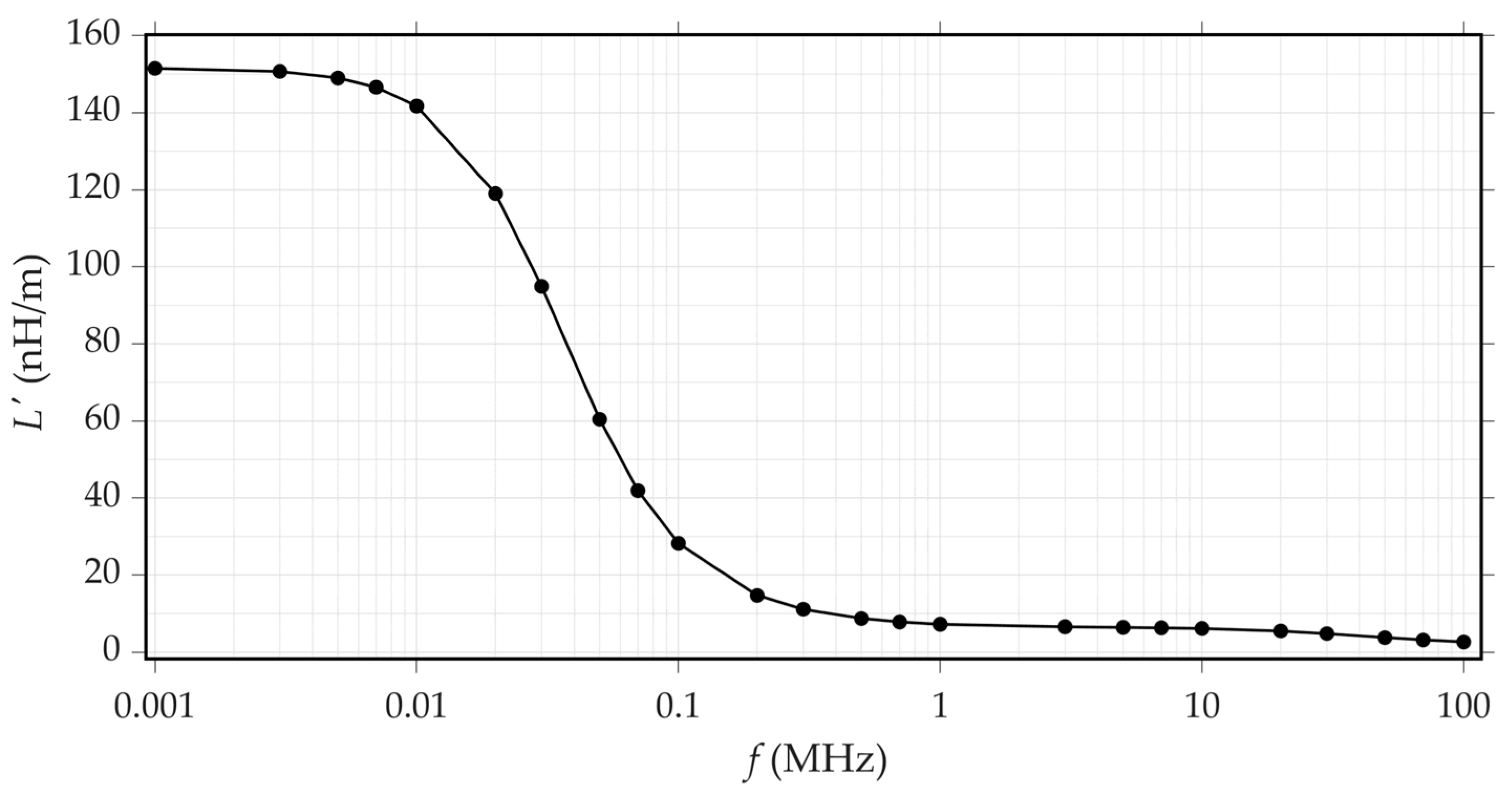
Let us denote the frequency characteristics of the resistance per unit length and inductance per unit length of Dumet wire by R = f ( f ) and L = f ( f ) , respectively. The mathematical model of the considered standard, presented in ref. [4], included these characteristics in the frequency range from 1 kHz to 1 MHz. To extend the frequency range of these characteristics up to 100 MHz, a FEM simulation model of a Dumet segment was performed in COMSOL Multiphysics using a 2D geometry. The resistance and inductance values per unit length were determined using the relations [28]:
R = 1 I 2 Q r d Ω ,
L = 2 I 2 W m d Ω ,
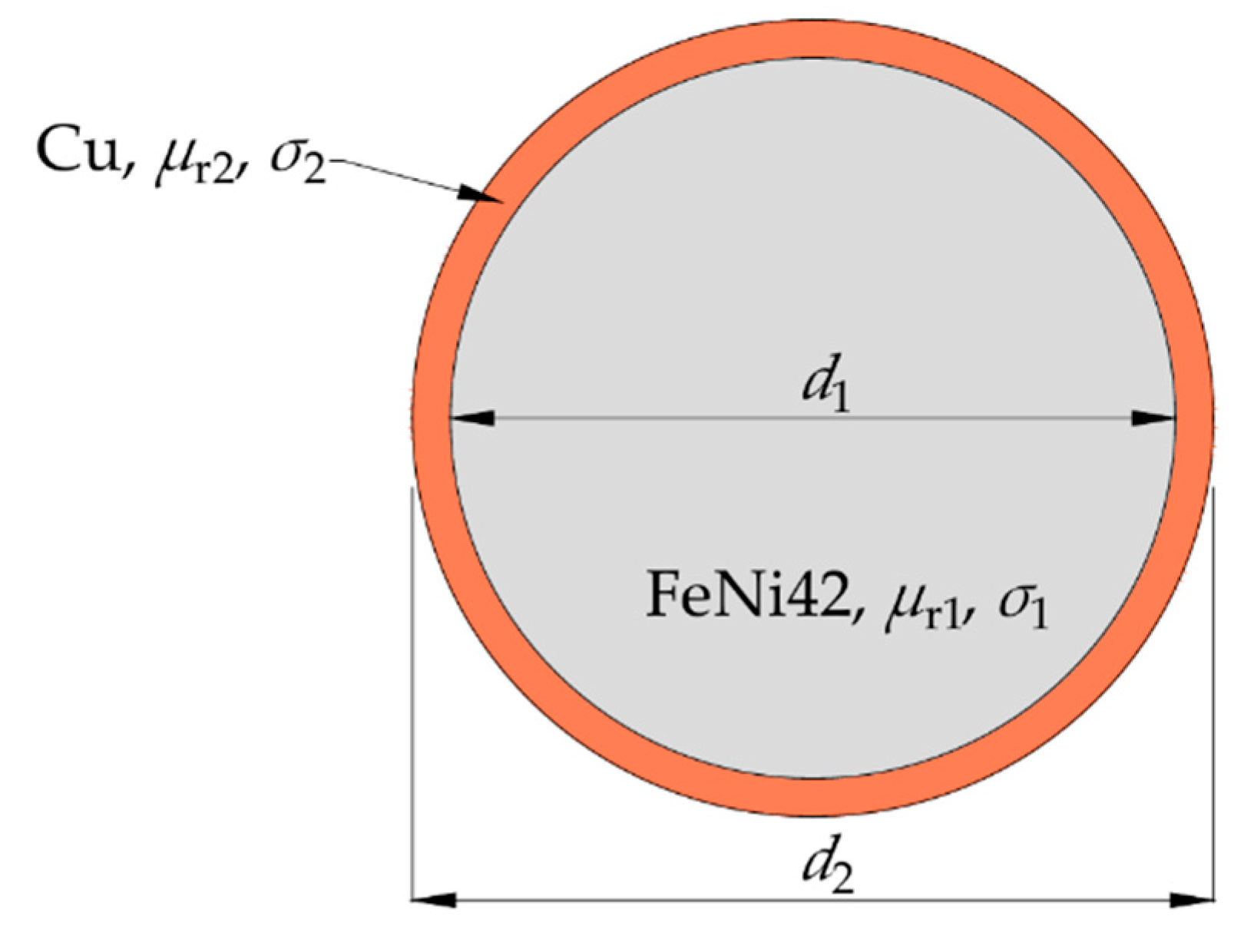
where I is the RMS value of the AC in the conductor, Q r is the Joule heat energy accumulated in the conductor cross-section under steady-state conditions, and W m is the magnetic energy density within the cross-section, also under steady-state conditions. The cross-section of the analyzed structure is shown in Figure 9.
The key parameters of FeNi42 and copper, relevant to the considered problem, are their magnetic permeabilities ( μ r 1 ( f ) and μ r 2 = 1 ) and electrical conductivities ( σ 1 = 1.4   MS / m and σ 2 = 58.4   MS / m ) [4], as well as the diameters d 1 = 456   μ m and d 2 = 504   μ m .
Since the magnetic permeability of FeNi42 varies with frequency, it was determined by interpolating the frequency characteristics μ r 1 ( f ) and μ r 1 ( f ) . The complex relative magnetic permeability is expressed as:
μ r 1 f = μ r 1 ( f ) j μ r 1 ( f ) ,
where μ r 1 is the real part and μ r 1 is the imaginary part of the relative permeability. The values of μ r 1 and μ r 1 were adopted from ref. [29].
In ref. [29], as manufacturers typically provide only a single-frequency value for permeability, a specialized two-step measurement and derivation technique was employed to obtain the full frequency characteristic. The experimental characterization was performed on an Alloy 42 lead frame, where a pair of parallel leads external to the package body was treated as a transmission line. The primary experimental data measured were the frequency-dependent resistance (R) and inductance (L) of this lead plus the return path across a broad spectrum from 0.1 MHz up to 1000 MHz. Crucially, the complex permeability was not measured directly. Instead, the experimental R and L characteristics were utilized in a 2-D electromagnetic simulator to solve the reverse problem. The simulator iteratively adjusted the real μ and imaginary μ″ parts of the complex permeability until the simulated R and L values matched the measured experimental data across the entire frequency range. This rigorous, frequency-sweeping derivation process ensures that the derived permeability is optimized for accurately modeling the high-frequency skin effect and inductance within the conductor geometry, maintaining consistency with the electromagnetic behavior of the Alloy 42 material up to 1 GHz.
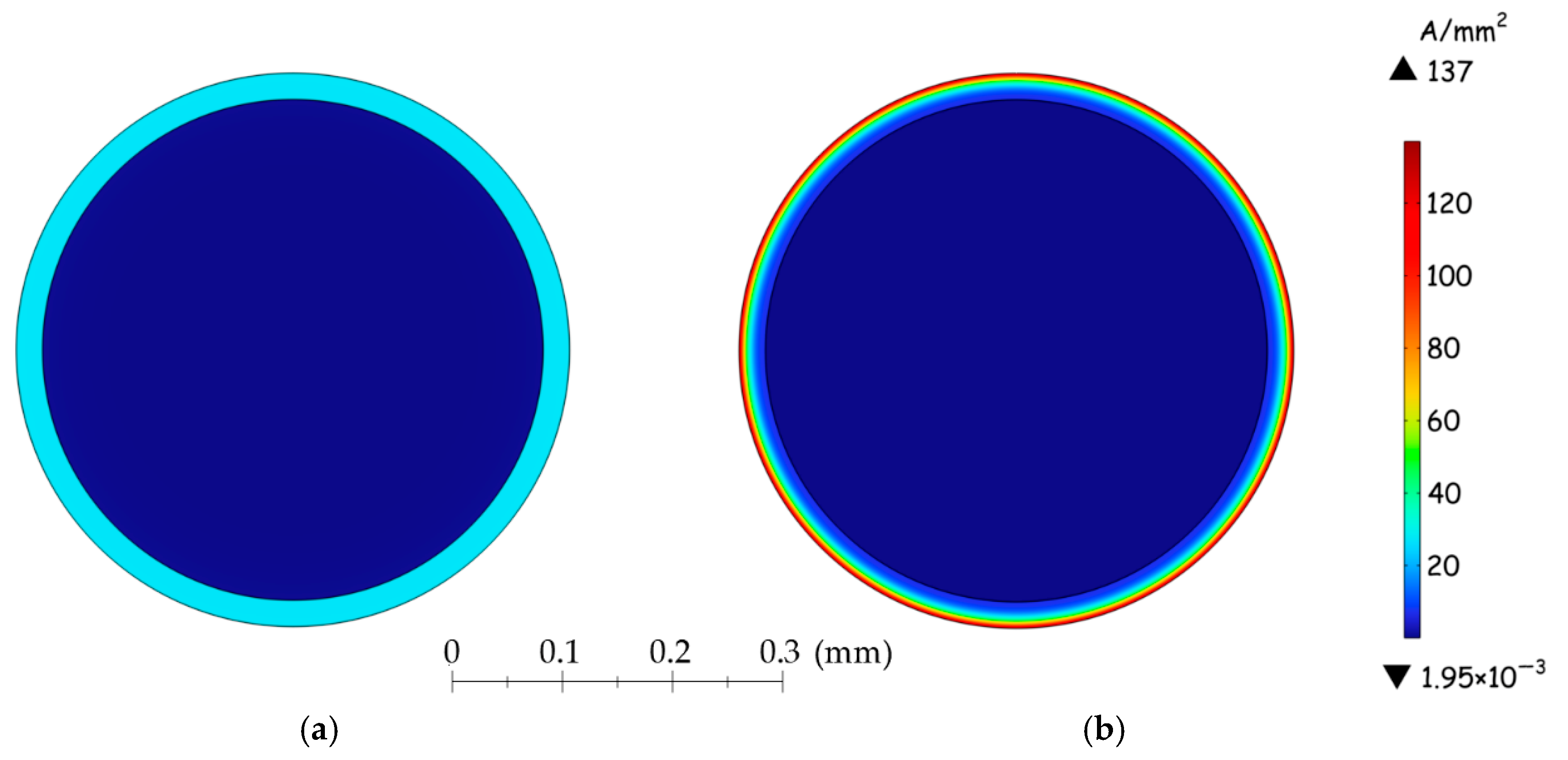
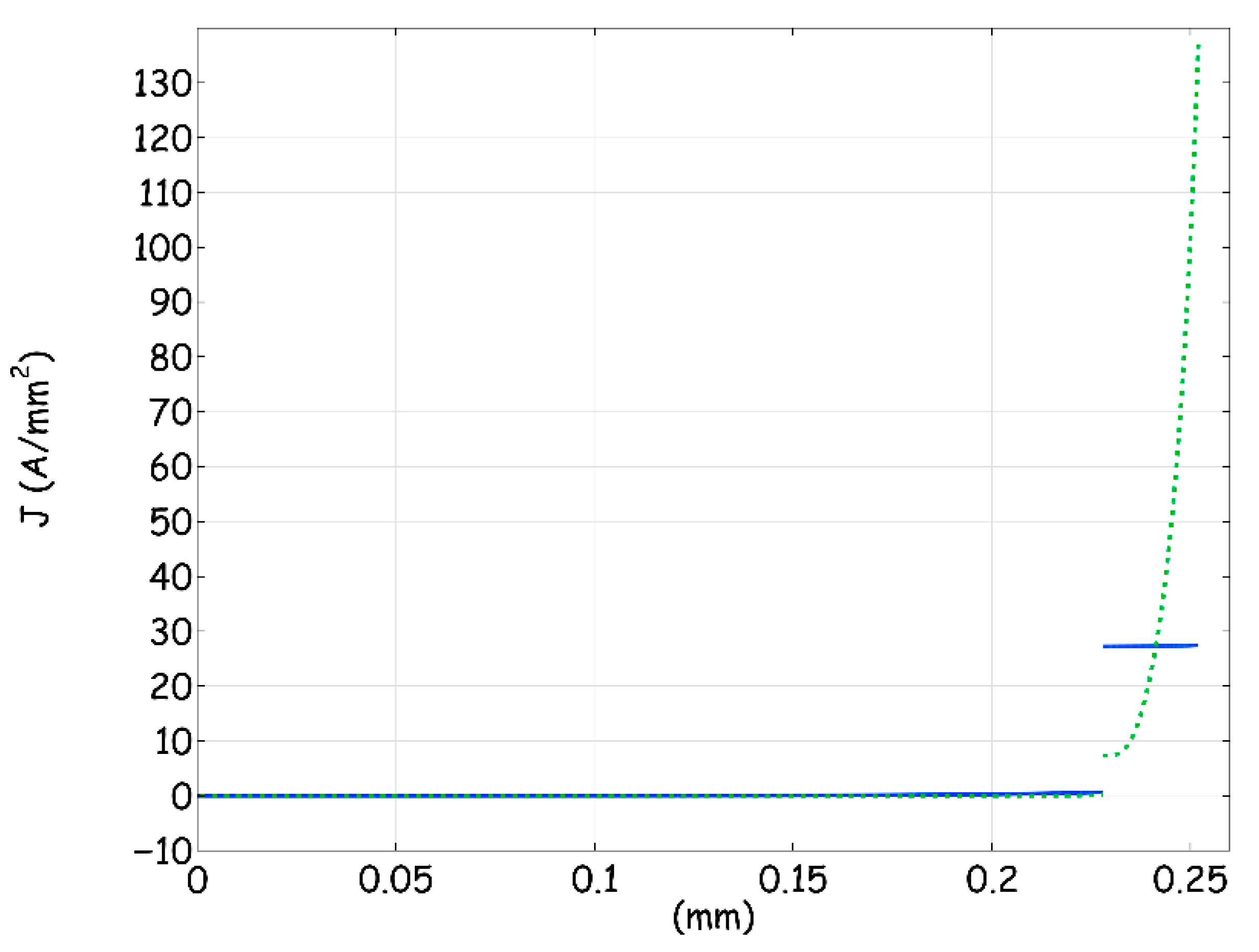
The magnetic permeability of FeNi42 varies nonlinearly with frequency: the real part μ r 1 decreases significantly, while the imaginary part μ r 1 reaches its maximum in the range of approximately 10–20 MHz. Figure 10 illustrates the distribution of the current density J within the Dumet wire cross-section for frequencies of 1 MHz and 100 MHz. Figure 11 presents the simulated distribution of the current density J along the diameter of the Dumet wire at two selected frequencies.
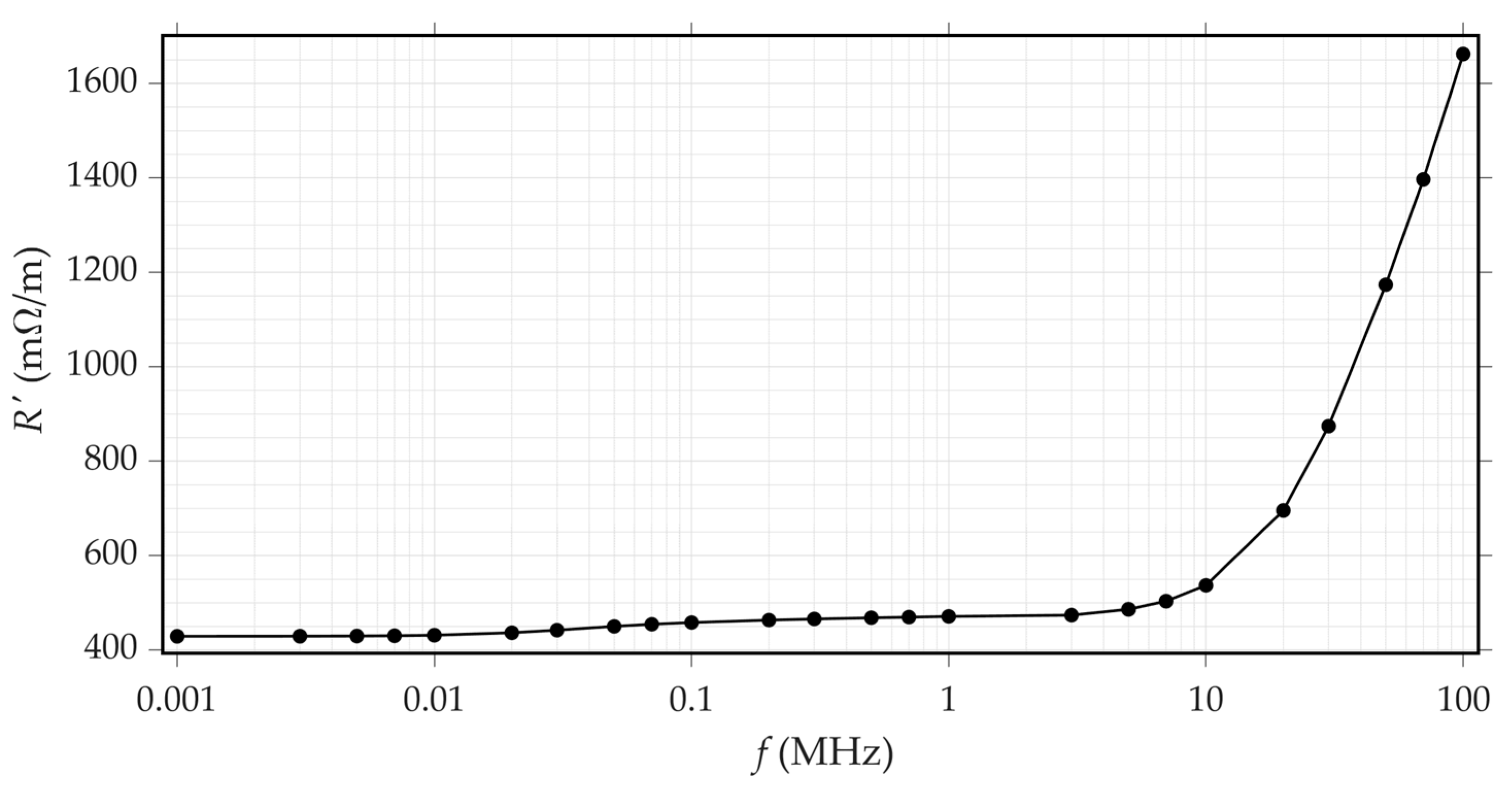
As shown in Figure 11, the maximum current density at 100 MHz is about five times higher than that at 1 MHz. For both 1 MHz and 100 MHz, the current density remains positive over the entire conductor cross-section and no reverse current component is observed. The results of the FEM simulation for the Dumet frequency characteristics are presented in Figure 12 and Figure 13.
As seen in Figure 12 and Figure 13, the resistance of Dumet begins to rise significantly above 10 MHz, while the inductance decreases sharply, particularly in the range 10–100 kHz. Both effects relate to the skin effect through the reduction in the effective conductor cross-section, as illustrated in Figure 10. The reduction of the inductance is further associated with the decrease in the FeNi42 magnetic permeability. The combined effect of these two phenomena results in a several dozen-fold decrease in inductance at 100 MHz compared with 1 kHz.

4.3. A New Impedance Approximation of the Housing

The approximation function used in ref. [4] for the enclosure impedance, expressed via Equation (12), ensured numerical stability of the model in the frequency range up to 1 MHz. However, this approach proved to be insufficient for extending the frequency range of the mathematical model beyond such a frequency. Moreover, a polynomial approximation of the modified Bessel functions may lead to significant inaccuracies.
To improve the numerical stability of the algorithm, as well as the accuracy and efficiency of the calculations, we begin with different formulations of the impedance of the enclosure [30]:
Z o = γ 2 π σ o r 1 I 0 γ r 1 K 1 γ r 2 + I 1 γ r 2 K 0 γ r 1 I 1 γ r 1 K 1 γ r 2 I 1 γ r 2 K 1 γ r 1 ,
where γ is the complex propagation constant, defined as [30]:
γ = j σ o μ 0 μ o ω ω 2 ε 0 ε o μ 0 μ o .
Since the value of σ o is sufficiently high, Equation (20) can be simplified to the form [31]:
γ = j σ o μ 0 μ o ω .
Formula (23) is still numerically unstable due to very high/very low results of the quotients and products of the modified Bessel functions. To avoid this issue, we propose in this article a scaling of the modified Bessel functions using their exponential equivalent. Equation (23) is then transformed by scaling the modified Bessel functions [32]:
I n s γ r = exp γ r I n γ r ,
K n s γ r = exp ( γ r ) K n ( γ r ) ,
where n denotes the order of the modified Bessel function (in the analyzed case, n = 0 or n = 1).
Substituting Equations (26) and (27) into (23) yields the final form of the function representing the enclosure impedance:
Z o = γ 2 π σ o r 1 I 0 s γ r 1 K 1 s γ r 2 exp γ ( r 1 r 2 ) + I 1 s γ r 2 K 0 s γ r 1 exp γ ( r 2 r 1 ) I 1 s γ r 1 K 1 s γ r 2 exp γ ( r 1 r 2 ) I 1 s γ r 2 K 1 s γ r 1 exp γ ( r 2 r 1 ) .
Equation (28) remains numerically stable even at high frequencies. This results from the fact that the subtraction of the radii in the argument of the scaling function reduces its magnitude, thereby limiting the occurrence of extreme numerical values and preventing numerical oscillations.
The scaled modified Bessel functions are computed from [33]:
I 0 s γ r 1 2 π γ r 1 + m = 1 NA c m γ r m ,
I 1 s γ r 1 2 π γ r 1 m = 1 NA d m γ r m ,
K 0 s γ r π 2 γ r 1 + m = 1 NA 1 m c m γ r m ,
K 1 s γ r π 2 γ r 1 m = 1 NA 1 m d m γ r m ,
where the parameters c m , d m , and NA are defined as [33]:
c m = 1 m 8 m m ! t = 1 m 2 t 1 2 ,
d m = 1 m + 1 8 m m ! t = 1 m 4 2 t 1 2 ,
NA = 12     f o r 25 < α r < 50 9     f o r 50 α r < 100 7     f o r 100 α r < 300 5     f o r 300 α r < 1000 3     f o r 10 , 000 α r ,
where the parameter α r is the product of the radius r (in the analyzed case r is equal r 1 or r 2 ) and the attenuation constant α, defined as [33]:
α = γ 1 + j = σ μ ω 2 .
The replacement of the (variable-precision floating-point numbers with 32 significant digits) approximation polynomial with a new formulation based on scaled modified Bessel functions significantly improved the model’s performance. This change reduced the average run-time for a single frequency point calculation by more than 30 times and eliminated the catastrophic numerical instability that previously occurred above 50 MHz.

4.4. Determination of the Conductivity of the N-Type Connector Pin–Cu1 Joint

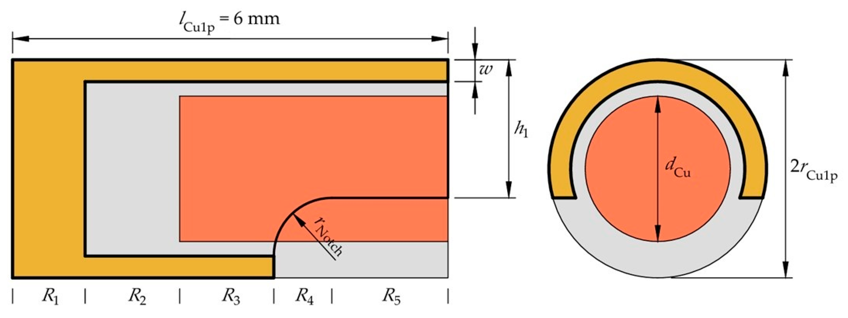
In the mathematical model presented in ref. [4], resistance R and impedance Z in the section of the brass pin of the N-type connector were calculated solely by considering the segment of the copper conductor located inside the pin cavity, neglecting the conductance of the pin itself and of the solder joint. This constituted a significant simplification. Figure 14 presents the cross-sectional schematic of the Cu1p section, showing the material distribution and section labeling.
To increase the accuracy of the mathematical model in the analyzed section of the standard, resistance R and impedance Z are calculated using the cross-sectional surface A Culp = π r Culp 2 and the length of the brass pin l Culp , as well as the resultant electrical conductivity σ Culp determined as:
σ Culp = l Culp R Culp π r Culp 2 ,
where the total resistance R Culp is the sum of the resistances R 1 R 5 of the individual sections of the Cu1p section in Figure 14:
R Culp = R 1 + R 2 + R 3 + R 4 + R 5 .
Resistances R 1 R 5 were calculated based on the corresponding lengths l R 1 l R 5 , representing each section, cross-sectional surfaces, and electrical conductivities of copper, brass, and soldering that are denoted, respectively, as σ Cu , σ Brass , and σ Sn60Pb40 . As an example, the resistance of section R 5 is determined as:
R 5 = 1 1 R 5 Brass + 1 R 5 Cu + 1 R 5 Sn60Pb40 ,
where
R 5 Brass = l R 5 σ Brass A r Culp , h 1 + A r Culp w , 2 r Culp h 1 w π r Culp w 2 ,
R 5 Cu = l R 5 σ Cu π d Cu 2 2 ,
R 5 Sn60Pb40 = l R 5 σ Sn60Pb40 π r 2 A r Culp , h 1 + A r Culp w , 2 r Culp h 1 w π r Culp w 2 π d Cu 2 2 ,
where, as depicted in Figure 14, d Cu is the diameter of the copper wire, w is the wall thickness of the brass pin, and h 1 represents the height of the circular segment measured from the chord to the arc of the brass pin in section R 5 . The parameter A r , h denotes a function describing the area of a circular segment:
A r , h = 1 2 r 2 2 arccos r h r sin 2 arccos r h r ,
where r is the radius of the disc and h is the height of the circular segment measured from the chord to the arc. The resistances R 1 , R 2 , and R 3 are calculated analogously to R 5 .
In the case of R 4 , due to the varying cross-sections of the brass and Sn60Pb40 alloy, the resistance is determined as:
R 4 = 0 l R 4 dx σ Cu π d Cu 2 2 + σ Sn60Pb40 A Sn60Pb40 x + σ Brass A Brass x ,
where
A Brass x = A r Culp , h x π ( r Culp w ) 2 + A r Culp w , 2 r Culp h x w ,
A Sn60Pb40 x = π r Culp 2 A Brass x π d Cu 2 2 ,
and x is a variable representing the position along section R 4 , with x ϵ 0 ,   l R 4 . The function h ( x ) describes the height of the circular segment measured from the chord to the arc of the circular segment corresponding to the notch in the brass connector pin (section R 4 ), and l R 4 is the length of R 4 section. Assuming that the notch shape is a circular fragment, h ( x ) is derived from the circle equation as follows:
h ( x ) = h 1 + r Notch r Notch 2 x 2 ,
where r Notch is the radius of the notch, as depicted in Figure 14.
Due to the complexity of the integral, the calculations were performed numerically in MATLAB. An advantage of this method is the possibility of estimating the uncertainty using the Monte Carlo method with generally available programming tools. The copper conductor segment soldered to the pin of the N-type connector (Cu1p) was presumed to be a cylinder with a diameter of 2 mm (the same as conductors Cu1 and Cu2) and a length of approximately 5 mm. The conductivity σ Culp is determined to be 15.3   MS / m and its uncertainty u ( σ Culp ) is 6.4   MS / m (for k = 2).

5. Results

The mathematical model, originally implemented in Wolfram Mathematica for its symbolic computation capability, was reimplemented in MATLAB to perform the millions of iterations required for a Monte Carlo uncertainty analysis.
This transition to MATLAB’s double-precision floating-point arithmetic caused a numerical overflow error. A local variable in the impedance calculation function exceeded its maximum permissible value at frequencies of 470 kHz and above, an issue not encountered in Mathematica’s symbolic environment. This was resolved by modifying the function that approximates the enclosure’s impedance.
Additionally, to improve consistency between DC and AC calculations, the original DC resistance formulas were replaced. The new method calculates DC resistance by taking the real part of the AC impedance formulas evaluated at a very low frequency (0.1 Hz). This aligns the methodologies for calculating both DC resistance and AC impedance.
The Monte Carlo method was used to evaluate the uncertainty of the calculated AC-DC transfer differences [25]. The input parameters were randomly sampled within their absolute error bounds, assuming a uniform distribution, except for two parameters—i.e., D Teflon and the thickness of the tee housing in the area with Teflon insulator—for which uncertainties were specified and a Gaussian distribution was applied. All the input parameters with their error bounds are listed in Appendix A.
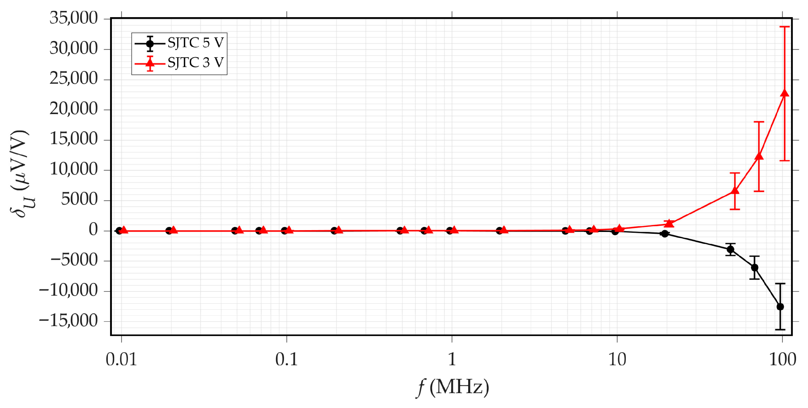
Figure 15 presents calculated AC-DC transfer differences obtained from the improved mathematical model of the SJTC 3 V and SJTC 5 V standards over the frequency range from 10 kHz to 100 MHz.
As shown in Figure 15, in the frequency range from 10 kHz to 100 MHz, both the transfer difference and its associated uncertainty increase with frequency for both standards. For the SJTC 3 V standard, the calculated transfer difference reaches 23,000 μV/V at 100 MHz, accompanied by an expanded uncertainty of 12,000 μV/V. In contrast, the SJTC 5 V standard exhibits a more gradual response, with the transfer difference reaching only −12,500 μV/V at the same frequency. Both standards maintain a relatively flat characteristic, with variations remaining within 300 μV/V up to approximately 10 MHz. Above 2 MHz, the AC-DC transfer difference of the SJTC 5 V standard transitions to negative values. Furthermore, the uncertainty for the SJTC 3 V standard is consistently higher, reaching 12,000 μV/V compared with 3900 μV/V for the 5 V standard, primarily due to the shorter enclosure amplifying boundary effects.
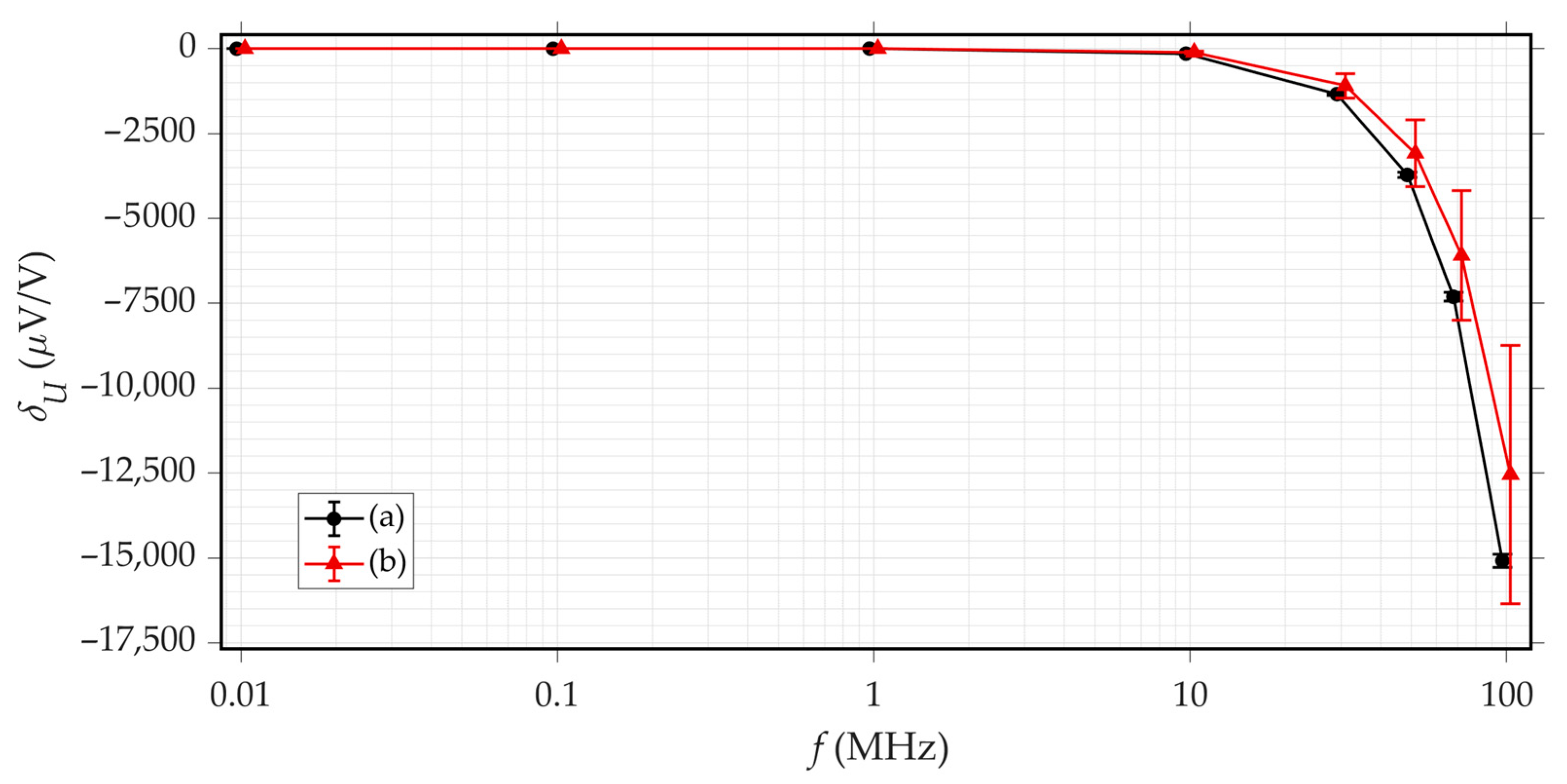
To validate the newly developed mathematical model, the SJTC 5 V TVC was compared with a CTVC developed at SUT [19]. All the measurements were performed in an electromagnetically shielded measurement chamber with a precisely controlled temperature (21 ± 0.1 °C) and measured humidity. The results of AC/DC transfer difference measurements performed at 3 V and in the frequency range from 10 kHz to 100 MHz are presented in Figure 16.
Figure 16 presents a comparison between the measured transfer difference and the values calculated using the improved model. In the frequency range up to approximately 10 MHz, the absolute difference between the modeled and measured AC-DC transfer differences remains below 2.5 μV/V, demonstrating excellent agreement. However, as the frequency increases, the discrepancy widens, reaching approximately 15 μV/V at 50 MHz and peaking at 42 μV/V at 100 MHz.
The method depicted in Figure 16 (red triangles), despite exhibiting higher uncertainties than the CTVC reference (black dots), is preferable in many contexts because its mathematical model has been substantially improved compared with previously existing models. The SJTC (Figure 16, red triangles) remains a standard widely used by the National Measurement Institutes (NMIs) worldwide due to its very low thermal time constant, high stability, and relatively low cost. In contrast, the CTVC (Figure 16, black dots) possesses a substantial thermal time constant—approximately 15 times higher than that of the SJTC—which can deteriorate measurement throughput and complicate automated calibration procedures [12].
This deviation in the 30–100 MHz range is attributed to three primary physical factors that are difficult to fully capture in the mathematical model. First, the transition zone between the N-type connector and the internal coaxial structure introduces parasitic stray capacitances and inductances. While the improved model accounts for the pin conductivity, the complex 3D geometry of the “launch” area creates small impedance mismatches that amplify transfer differences as the wavelength shortens. Moreover, the model assumes perfect electrical contact between the materials, which can slightly deviate the results at higher frequencies.
Second, the finite element method (FEM) simulations for the Dumet wire leads were performed using 2D axial symmetry. In the actual physical realization, the heater leads must be bent to accommodate the housing, and the solder joints possess irregular shapes. These 3D geometric asymmetries introduce non-coaxial electromagnetic field components that become significant contributors to the transfer difference only at frequencies exceeding 30 MHz. Finally, the dielectric properties of the glass bead sealing the SJTC element (section 8) are assumed to be constant. In reality, the dielectric loss tangent of the glass likely increases in the VHF range, leading to additional AC energy dissipation that is not present in the DC regime, thereby contributing to the observed divergence.
In addition, above approximately 30 MHz, a sharp increase in the uncertainty of the model-based results is observed. Despite these discrepancies, the overlap of the expanded uncertainty intervals (k = 2) indicates that the measured and modeled results are consistent within their estimated uncertainties.

6. Conclusions

This study presented a comprehensive modification of the mathematical model for a calculable SJTC, successfully extending its operational frequency range from 1 MHz to 100 MHz. The limitations of the previous model, specifically regarding computational inefficiency and numerical instability at higher frequencies, were effectively addressed.
The key improvements included the re-evaluation of the Dumet wire leads’ characteristics through FEM simulations, which accounted for the skin effect and the frequency-dependent magnetic permeability of the FeNi42 core. Additionally, the numerical stability of the algorithm was significantly enhanced by replacing the polynomial approximation of the housing impedance with a new formulation based on scaled modified Bessel functions. The model’s accuracy was further refined by incorporating the detailed geometry and electrical conductivity of the N-type connector’s central pin and solder joint.
The improved model was validated by comparing calculated AC-DC transfer differences with experimental measurements of a 5 V nominal voltage standard. The results demonstrated good agreement between the theoretical and measured data, particularly in the frequency range up to 10 MHz. Although discrepancies increased at frequencies above 30 MHz due to unmodeled parasitic reactances and 3D geometric effects, the modeled results remained consistent with measurement data within the expanded uncertainty intervals (k = 2).
The reimplementation of the model in MATLAB facilitated robust uncertainty evaluation using the Monte Carlo method, establishing this refined model as a valuable tool for optimizing the design and ensuring the traceability of thermal AC voltage standards in the high-frequency regime.

Author Contributions

K.K. and M.K.: conceptualization and methodology, analysis of results, funding acquisition, supervision, review, and corrections. M.P.: investigations, visualization, original draft preparation, and writing. All authors have read and agreed to the published version of the manuscript.

Funding

This work was supported by the Polish National Science Centre (NCN, grant no. 2022/47/B/ST7/00047).

Data Availability Statement

The original contributions presented in this study are included in the article. Further inquiries can be directed to the corresponding author.

Conflicts of Interest

The authors declare no conflicts of interest. The funders had no role in the design of the study, in the collection, analyses, or interpretation of data, in the writing of the manuscript, or in the decision to publish the results.

Appendix A

This appendix contains model input parameters for the SJTC 5 V used in Monte Carlo simulations. The parameters are listed in Table A1.
Table A1. Model input parameters for the SJTC 5 V.
ParameterValueMaximum Permissible Error
Electrical conductivity of the enclosures of the N-type input connector and the tee9.3 MS/m2.3 MS/m
Electrical conductivity of the internal wires of the N-type input connector and the tee9.3 MS/m2.3 MS/m
Electrical conductivity of the closing disks14.9 MS/m0.05 MS/m
Electrical conductivity of the enclosure46 MS/m4 MS/m
Electrical conductivity of the Cu1 and Cu2 wires57 MS/m3 MS/m
Electrical conductivity of the resistive wire0.77 MS/m0.06 MS/m
Electrical conductivity of the heater of the TVC0.752 MS/m0.003 MS/m
Thickness of the tee enclosure for the section with air insulation4 mm1 mm
Thickness of the enclosure closing disks10.0 mm0.1 mm
Thickness of the enclosure2.0 mm0.3 mm
Length of the section in the N-type input connector and tee with air insulation18 mm1 mm
Length of the section in the N-type tee connector with teflon insulation7 mm1 mm
Length of the section in the N-type input connector with teflon insulation17 mm1 mm
Length of the Cu1 wire9 mm1 mm
Length of the resistive wire132 mm1 mm
Length of the Cu2 wire4 mm1 mm
Length of the leads of the TVC8.7 mm1 mm
Length of the heater of the TVC6.6 mm1 mm
Length of the Cu3 wire3 mm1 mm
Diameter of the N-type tee enclosure17 mm0.6 mm
Diameter of the inner wires of the N-type input connector and tee 3.04 mm0.02 mm
Inner diameter of the enclosure in the section with air insulation in the N-type input connector and tee7 mm0.02 mm
Inner diameter of the enclosure60.0 mm0.2 mm
Diameter of the Cu1 and Cu2 wires0.5 mm0.1 mm
Diameter of the resistive wire150.4
Diameter of the Cu3 wire2.3 mm0.1 mm
Resistance of the TVC heater90 Ω10 Ω

References

  1. Shan, Y.; Meng, Y.S.; Filipski, P.S. Evaluation of a Calorimetric Thermal Voltage Converter for RF–DC Difference up to 1 GHz. IEEE Trans. Instrum. Meas. 2013, 63, 467–472. [Google Scholar] [CrossRef]
  2. Lipe, T.E.; Kinard, J.R.; Tang, Y.-H.; Benz, S.P.; Burroughs, C.J.; Dresselhaus, P.D. Thermal Voltage Converter Calibrations Using a Quantum ac Standard. Metrologia 2008, 45, 275–280. [Google Scholar] [CrossRef]
  3. Musioł, K. Experimental Study of Digitizers Used in High-Precision Impedance Measurements. Energies 2022, 15, 4051. [Google Scholar] [CrossRef]
  4. Grzenik, M.; Kampik, M. Calculable AC Voltage Standards for 10 kHz-1 MHz Frequency Range. IEEE Trans. Instrum. Meas. 2016, 66, 1372–1378. [Google Scholar] [CrossRef]
  5. Pogliano, U.; Bosco, G.C. Determination of the Frequency Dependence of the AC–DC Voltage Standard at IEN. IEEE Trans. Instrum. Meas. 2002, 51, 373–376. [Google Scholar]
  6. Amagai, Y.; Kato, H.; Makino, T.; Shimizume, K.; Okawa, K.; Muramatsu, H.; Sakamoto, N.; Kaneko, N.-H. Heat Transfer Analysis of a Diamond Chip Resistor in Planar Multijunction Thermal Converters. In Proceedings of the 2024 Conference on Precision Electromagnetic Measurements (CPEM), Denver, CO, USA, 8–12 July 2024; pp. 1–2. [Google Scholar]
  7. Fujiki, H.; Amagai, Y.; Shimizume, K.; Kishino, K.; Hidaka, S. Fabrication of Thin Film Multijunction Thermal Converters with Improved Long-Term Stability. IEEE Trans. Instrum. Meas. 2015, 64, 2389371. [Google Scholar] [CrossRef]
  8. Amaga, Y.; Fujiki, H.; Shimizume, K.; Hidaka, S. Improved Stability of Thin-Film Multijunction Thermal Converters. Electr. Eng. Jpn. 2014, 188, 18–26. [Google Scholar] [CrossRef]
  9. Amagai, Y.; Okawa, K.; Sakamoto, N.; Kaneko, N.-H. Highly Accelerated Life Testing of Bi–Sb Thermocouples in Planar Multijunction Thermal Converters. In Proceedings of the 2024 Conference on Precision Electromagnetic Measurements (CPEM), Denver, CO, USA, 8–12 July 2024; pp. 1–2. [Google Scholar]
  10. Amagai, Y.; Okawa, K.; Sakamoto, N.; Kaneko, N.-H. Signal-to-Noise Ratio Optimization for Planar Multijunction Thermal Converters. IEEE Trans. Instrum. Meas. 2023, 72, 1003507. [Google Scholar] [CrossRef]
  11. Hidaka, S.; Kishino, K.; Shimizume, K.; Takeda, S.; Fujiki, H.; Amagai, Y.; Sasaki, H. Multijunction Thermal Converter with Improved Frequency Characteristics Between 10 Hz and 1 MHz. IEEJ Trans. Electr. Electron. Eng. 2012, 8, 101–104. [Google Scholar] [CrossRef]
  12. Filipski, P.; Clark, R.; Paulusse, D. Calorimetric Thermal Voltage Converter as a Wideband Calculable Standard of AC-DC Difference. IEEE Trans. Instrum. Meas. 2002, 48, 387–390. [Google Scholar] [CrossRef]
  13. Kubiczek, K.; Kampik, M.; Musioł, K. Calorimetric Thermal Voltage Converter with a Microwave Disk Resistor as a Heater. IEEE Trans. Instrum. Meas. 2025, 74, 1504707. [Google Scholar] [CrossRef]
  14. Kubiczek, K.; Kampik, M.; Grzenik, M. Analysis of DC Reversal Error of the Calorimetric Thermal Voltage Converter. Measurement 2021, 168, 108439. [Google Scholar] [CrossRef]
  15. Filipski, P.S.; Clark, R.F.; Paulusse, D.C. Evaluation of LF AC–DC Difference of Coaxially Mounted Thermal Voltage Converter. In Proceedings of the IMTC’97—Instrumentation and Measurement Technology Conference, Ottawa, ON, Canada, 19–21 May 1997; pp. 720–725. [Google Scholar]
  16. COMSOL Multiphysics®, Version 6.3; COMSOL AB: Stockholm, Sweden, 2024; Available online: https://www.comsol.com (accessed on 24 October 2025).
  17. MATLAB, Version R2023b; The MathWorks, Inc.: Natick, MA, USA, 2023; Available online: https://www.mathworks.com (accessed on 24 October 2025).
  18. Kampik, M.; Grzenik, M.; Lippert, T.; Rydler, K.-E.; Tarasso, V.; Trinchera, B. Comparison of a Thermal AC Voltage Standard in the 1–30-MHz Frequency Range. IEEE Trans. Instrum. Meas. 2020, 70, 1500508. [Google Scholar] [CrossRef]
  19. Kubiczek, K.; Grzenik, M.; Kampik, M. Frequency-dependent component of AC-DC transfer difference of a redesigned calorimetric thermal converter. Measurement 2024, 226, 114136. [Google Scholar] [CrossRef]
  20. Department of Defense. MIL-STD-348B: Department of Defense Interface Standard—Radio Frequency Connector Interfaces for MIL-DTL-3643, MIL-DTL-3650, MIL-DTL-3655, MIL-DTL-25516, MIL-PRF-31031, MIL-PRF-39012, MIL-PRF-49142, MIL-PRF-55339, MIL-DTL-83517; Department of Defense: Washington, DC, USA, 2014. [Google Scholar]
  21. Carpenter Electrification. Evanohm® R—Data Sheet; Carpenter Electrification: Philadelphia, PA, USA, 2025. [Google Scholar]
  22. Malinowski, M.; Kubiczek, K.; Kampik, M. A Precision Coaxial Current Shunt for Current AC-DC Transfer. Measurement 2021, 176, 109126. [Google Scholar] [CrossRef]
  23. Dwight, H.B. Reactance and skin effect of concentric tubular conductors. Electr. Eng. 1942, 61, 513–518. [Google Scholar] [CrossRef]
  24. Mingli, W.; Yu, F. Numerical calculations of internal impedance of solid and tubular cylindrical conductors under large parameters. Iee. Proc. Gener. Transm. Distrib. 2004, 151, 67–72. [Google Scholar] [CrossRef]
  25. JCGM. Evaluation of Measurement Data—Supplement 1 to the “Guide to the Expression of Uncertainty in Measurement”—Propagation of Distributions Using a Monte Carlo Method, JCGM 101:2008; BIPM: Sèvres, France, 2008; Available online: https://www.bipm.org/en/publications/guides (accessed on 12 September 2025).
  26. Pasternack—Coaxial Cable Impedance Calculator with Formula. Available online: https://www.pasternack.com/t-calculator-coax-cutoff.aspx (accessed on 12 September 2025).
  27. Pasternack Enterprises, Inc. PE9390—N Tee Adapter Male-Male-Male, Datasheet; Pasternack Enterprises, Inc.: Irvine, CA, USA, 2012. [Google Scholar]
  28. COMSOL Inc. AC/DC Module—User’s Guide, Version 6.3; COMSOL Inc.: Burlington, VT, USA, 2024. [Google Scholar]
  29. Young, B. Determination of the frequency-dependent complex permeability of Alloy 42. In Proceedings of the 44th Electronic Components and Technology Conference, Washington, DC, USA, 1–4 May 1994. [Google Scholar]
  30. Vujevic, S.; Lovric, D.; Boras, V. High-Accurate Numerical Computation of Internal Impedance of Cylindrical Conductors for Complex Arguments of Arbitrary Magnitude. IEEE Trans. Electromagn. Compat. 2014, 56, 1431–1438. [Google Scholar] [CrossRef]
  31. Kubiczek, K.; Kampik, M. Fast and Numerically Stable Analytical Computations for the Power Induced in Cylindrical Multilayered Conductors Under External Magnetic Fields. IEEE Trans. Electromagn. Compat. 2022, 65, 292–299. [Google Scholar] [CrossRef]
  32. Kubiczek, K. Computation of the Characteristic Parameters of Coaxial Waveguides Used in Precision Sensors. Sensors 2023, 23, 2324. [Google Scholar] [CrossRef] [PubMed]
  33. Vujevic, S.; Lovric, D. On the numerical computation of cylindrical conductor internal impedance for complex arguments of large magnitude. Facta Univ. Ser. Electron. Energetics 2016, 30, 81–91. [Google Scholar] [CrossRef]
Figure 1. Schematic diagram illustrating the principle of operation of AC–DC transfer measurements.
Energies 19 00062 g001
Figure 2. Cross-section diagram of the SJTC type TVC standard according to ref. [4].
Energies 19 00062 g002
Figure 3. N-type tee connector used.
Energies 19 00062 g003
Figure 4. SJTC-type TVC standard of UN = 1.5 V, after partial disassembly of the housing. Due to its small diameter, the resistance wire is not visible in the figure.
Energies 19 00062 g004
Figure 5. Close-up of the standard’s SJTC after partial disassembly of the housing.
Energies 19 00062 g005
Figure 6. Two-port network describing a single region of the standard model.
Energies 19 00062 g006
Figure 7. Schematic diagram of a single coaxial area of the standard model. Its description is given in the text.
Energies 19 00062 g007
Figure 8. Schematic of the cross-section of the N-type T-connector, based on various sources [20,26,27].
Energies 19 00062 g008
Figure 9. Cross-section of the SJTC lead made of Dumet.
Energies 19 00062 g009
Figure 10. Distribution of current density J in the Dumet cross-section for (a) 1 MHz and (b) 100 MHz. The current density is given in units of A/m2.
Energies 19 00062 g010
Figure 11. Distribution of the current density J along the diameter of the Dumet wire cross-section at 1 MHz (blue line) and 100 MHz (green dotted line). The current density is expressed in units of A/m2. The x-axis corresponds to Figure 10.
Energies 19 00062 g011
Figure 12. Frequency characteristic of the resistance per-unit length resistance of the Dumet wire.
Energies 19 00062 g012
Figure 13. Frequency characteristic of the inductance per unit length of the Dumet wire.
Energies 19 00062 g013
Figure 14. Cross-sectional schematic of the Cu1p area, with brass highlighted in yellow, copper in orange, and the Sn60Pb40 alloy in gray, with division into sections r 1 r 5
Energies 19 00062 g014
Figure 15. Frequency characteristics of the transfer difference obtained from the improved mathematical model for the SJTC 3 V and SJTC 5 V standards in the frequency range from 10 kHz to 100 MHz. The vertical bars represent expanded (k = 2) uncertainties. The frequency values are slightly shifted for better readability.
Energies 19 00062 g015
Figure 16. Comparison of the (a) measured (against calculable CTVC) [19] and (b) calculated values of SJTC 5 V standard. The vertical bars represent expanded (k = 2) uncertainties. The frequency values are slightly shifted for better readability.
Energies 19 00062 g016
Disclaimer/Publisher’s Note: The statements, opinions and data contained in all publications are solely those of the individual author(s) and contributor(s) and not of MDPI and/or the editor(s). MDPI and/or the editor(s) disclaim responsibility for any injury to people or property resulting from any ideas, methods, instructions or products referred to in the content.