Abstract
Full-bridge resonant converters have gained widespread adoption due to their excellent performance characteristics. However, these converters face limitations in terms of gain expansion. To address this issue, this paper proposes a switch-multiplexed resonant converter with wide voltage gain. By employing an auxiliary capacitor and inductor, the converter can achieve pseudo partial power processing and effectively expand its voltage gain. To regulate the voltage of the converter, the duty cycle of the switching devices is designed to be modulated, which is different from the conventional resonant converter. By optimizing the design parameters, the resonant current of converter can operate in discontinuous current mode (DCM), eliminating reverse recovery losses and/or minimizing reactive current. All switching devices achieve soft switching, thereby removing switching losses and further enhancing efficiency. Finally, a 1 kW prototype is built to validate the effectiveness of the proposed converter.
1. Introduction
With the increasing urgency of energy demands and environmental challenges, distributed power systems have become a focal point in energy research because of their flexibility, reliability, and environmentally friendly characteristics. The DC-DC converter is a critical unit in distributed power systems, influencing their operational stability and reliability [1,2,3].
DC-DC converters can be approximately categorized into pulse width modulation (PWM) converters and resonant converters. Common PWM converters include the buck converter [4], boost converter [5], forward converter [6], and flyback converter [7], etc. These converters regulate the voltage gain by modifying the pulse width of the modulation signal. Their features utilize simple structures and ease of modulation, leading to significant challenges in achieving soft switching. This issue impacts their overall conversion efficiency. Resonant converters can achieve soft switching and easy control. Common resonant converters include LC and LLC converters. LLC resonant converters have gained widespread application due to their ability to achieve zero voltage switching (ZVS) and zero current switching (ZCS) across the entire load range, coupled with their high conversion efficiency. The LLC resonant converters employ pulse frequency modulation to control voltage gain [8]. When wide voltage gain is required, the switching frequency should deviate from the resonant frequency, leading to decreased efficiency. To enhance converter performance, researchers have modified the resonant converter structure, proposing a two-stage configuration. Refs. [9,10,11,12,13] combined the LLC resonant converter with a buck converter, where the buck converter serves as a voltage regulator in the front-end stage. The LLC resonant converter operates at its resonant point, providing electrical isolation and high-efficiency energy transfer. However, this two-stage structure results in relatively low system efficiency. And the large number of switching devices in two-stage converters limits improvements in power density. To enhance energy conversion efficiency and enable voltage gain regulation, Refs. [14,15,16,17] proposed a topology where the LLC converter is connected in parallel with a voltage gain regulation stage. The LLC stage handles the majority of power transfer, while the regulation stage adjusts the overall voltage gain of the topology. During regulation, this structure achieves high energy conversion efficiency and voltage regulation capability. However, when this topology uses buck or boost converters to regulate the output voltage, the electrical isolation capability is lost [18]. To reduce the number of switching devices, Refs. [19,20] proposed a switch-multiplexed two-stage buck-dual active bridge converter. Yet the two-stage structure, which offers advantages in the power characteristics of the buck inductor section, is currently only applied to dual active bridge converters and has not been extended to resonant converters. Under switch-multiplexing conditions, the input voltage is constrained because voltage gain must be adjusted through duty cycle modulation. This presents a significant challenge when applied to resonant converters, as achieving full-range soft switching for all switches remains an important research goal.
In recent years, the academic community has proposed a variety of converter topologies for achieving wide voltage gain and soft switching. For instance, Wu et al. proposed a fixed-frequency PWM-controlled bidirectional current-source soft-switching series resonant converter for energy storage applications in [21]. This converter can achieve full-range soft switching, but its current-source structure is relatively complex. Zuo et al. presented a fixed-frequency dual-PWM interleaved boost LLC resonant converter for photovoltaic applications in [22]. While this converter features a wide input voltage range, the interleaved structure increases the number of components. Gu et al. proposed a reconfigurable current-source LLC resonant converter based on cyclic PWM control in [23], which also offers a wide voltage gain range but requires complex reconfiguration logic. These existing topologies each have their advantages, yet they generally suffer from problems such as a large number of devices, complex control, or limited application scenarios.
To achieve wide voltage gain, this paper proposes a modified resonant converter with switch multiplexing. By multiplexing the switch, the proposed converter topology does not require additional switches. By employing the auxiliary capacitor and inductor, the converter can modulate the duty cycle of the multiplexed switches and process partial power in the switches network, leading to wide voltage gain. In addition, the proposed converter can operate in discontinuous current mode, and soft switching can be realized. In addition, compared with traditional partial power converters, the topology proposed in this paper also has advantages in terms of electrical isolation characteristics. Traditional partial power converters improve energy conversion efficiency, but auxiliary converters that transfer part of the power cause the entire converter to lose electrical isolation. In the converter proposed in this paper, the current flowing through the auxiliary converter section also passes through the transformer, ensuring the overall electrical isolation characteristics of the converter. In this paper, Section 2 analyzes the topology structure and the operation principle of the proposed converter. Section 3 analyzes the characteristics of the converter in detail, including the voltage gain, soft-switching condition and the pseudo partial power feature. Section 4 is the parameters design of the converter. Section 5 builds the prototype to verify the effectiveness of the proposed converter and its operating performance.
2. Topology and Principle Analysis of the Proposed Converter
2.1. Topology of the Proposed Converter
The switch-multiplexed LC resonant converter proposed in this paper is shown in Figure 1. Vin is the input voltage of the battery and Vout is the output voltage. The primary side of the converter consists of an inverter bridge formed by S1~S4, auxiliary inductor L1, auxiliary capacitor C2, and DC-blocking capacitor C3. The secondary side comprises a rectifier bridge formed by diodes D1~D4, resonant inductor L2, and resonant capacitor C4. The current through auxiliary inductor L1 is defined as i0. The transformer has a turns ratio of n:1. The primary ports of the transformer are defined as AB, with the current through these ports defined as i1. The secondary ports of the transformer are defined as CD, with the current through these ports defined as i2.
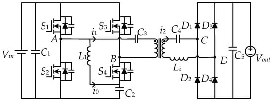
Figure 1.
The proposed switch-multiplexed resonant converter topology.
As for the proposed resonant converter, switches S1 and S2, auxiliary inductor L1, and auxiliary capacitor C2 constitute a buck converter. Specifically, the voltage of the auxiliary capacitor C2 can be regulated by adjusting the duty cycle of switches S1 and S2. When the converter works, part of the converter’s power is transferred through the auxiliary inductor L1. And by modulating the duty cycle of the multiplexed switches S1 and S2, the magnitude of the current of L1 can be controlled, which means that the power transferred by L1 is also changed. Then, the total power transferred by the converter can be adjusted to regulate the output voltage, which is the so-called pseudo partial power transmission.
The L1/C2 buck stage influences the full-bridge inverter by modifying the voltage amplitude at the midpoint of the primary side inverter bridge (VAB). Specifically, when S1 is turned on, the input voltage Vin charges the auxiliary capacitor C2 through L1, increasing VC2. When S2 is turned on, C2 discharges through L1. By adjusting the duty cycle D of S1 and S2, VC2 can be stably controlled at a specific value. This VC2 is superimposed on the input voltage to form the effective voltage of the full-bridge inverter, thereby changing the voltage gain of the converter. This mechanism avoids the need for additional independent voltage regulation stages, reducing component count and improving integration.
2.2. Operating Principle of the Topology
To analyze the topology conveniently, the parameters of the converter are defined. The operating frequency of the converter is defined as fs, and the time of one cycle-switching period is defined as Ts. The ratio of the conduction time of S1 and S2 to the switching period is defined as the duty cycle D. fr is the resonant frequency of the converter and defined as follows:
The operating waveforms of the converter are shown in Figure 2.
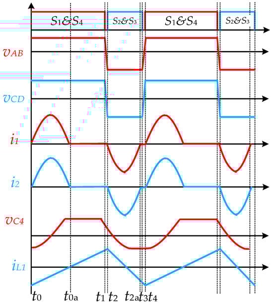
Figure 2.
The operation waveforms of the proposed converter.
In Figure 2, vAB is the input voltage, vCD is the output voltage, i1 is the current on the primary side of the transformer, i2 is the current on the secondary side of the transformer, vC4 is the voltage across the resonant capacitor, and iL1 is the current through the auxiliary inductor.
As shown in Figure 3, switches S1 and S4 operate simultaneously and switches S2 and S3 operate simultaneously. Primary side input voltage Vin transfers energy to capacitor C2 through the multiplexed switches S1 and S2 and the auxiliary inductor L1. When the duty cycle D changes, the voltage VC2 across the auxiliary capacitor C2 also changes accordingly. This subsequently alters the voltage amplitude VAB at the midpoint of the primary side inverter bridge, and the converter gain also changes. Consequently, part of the energy in this converter is transferred through the auxiliary inductor L1, while another portion is directly transferred through the inverter bridge. The specific operating mode of the converter is described as follows.
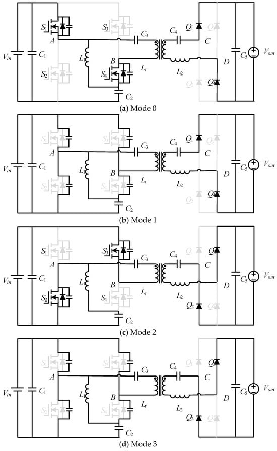
Figure 3.
The equivalent circuit of the proposed converter for different operation modes.
Mode 0 (t0~t1): As shown in Figure 3a, at time t0, switch S1 turns on at zero voltage and switch S4 turns on at zero current. The input power supply delivers energy to capacitor C2 through inductor L1. At this point, the primary voltage of the topology equals the input supply voltage plus the voltage across capacitor C2. Between time t0 and t0a, the primary current of the transformer is not zero and the primary side transfers energy to the secondary side through the resonant unit.
Mode 1 (t1~t2): As shown in Figure 3b, at time t1, switches S1 and S4 turn off, and all switches are in the off state. This time interval is referred to as the dead time. The energy stored in the parasitic capacitance of switch S2 is released through inductor L1 into capacitor C2, thereby providing the conditions for the zero-voltage turn-on of S2 in the next interval.
Mode 2 (t2~t3): As shown in Figure 3c, at time t2, switch S2 turns on at zero voltage and switch S3 turns on at zero current. At this time, the primary side voltage of the topology equals the negative supply voltage. The primary side transfers energy to the secondary side through the resonant unit. Between time t2 and t2a, the primary current of the transformer is not zero and the primary side transfers energy to the secondary side through the resonant unit.
Mode 3 (t3~t4): As shown in Figure 3d, at time t3, switches S2 and S3 turn off. Similarly to Mode 1, the energy stored in the parasitic capacitance of switch S1 is released through inductor L1 into capacitor C2, thereby enabling zero-voltage turn-on for S1 in the next interval.
3. Characteristics Analysis of the Proposed Converters
3.1. Voltage Gain Analysis of the Converter
The voltage gain of the converter can be calculated based on the principle that the power at the input and output terminals of a converter is approximately equal. The expression for the input power on the primary side of the converter is derived as follows,
where the values of are Vin − VC2, and the values of are −Vin. The current i2 during t0~t0a is opposite to the current during t2~t2a, which is shown as follows,
Then, according to Equation (3), Equation (2) can be obtained as follows:
The expression for the secondary output power of the converter can be derived as follows:
where the values of are Vout, and the values of are −Vout. The current i2 during t0~t0a is opposite to the current during t2~t2a, which is shown as follows,
The relation between i1 and i2 can be expressed as follows:
Then, the output power can be calculated as follows:
Because the input power and output power are equal, which is shown as follows:
The voltage gain of the converter can be obtained as follows:
where VC2 is the output voltage of buck converter. And the voltage of C2 can be adjusted by modulating the duty cycle of the multiplexed switches S1 and S2, which can be expressed as follows:
According to Equations (10) and (11), the voltage gain M can be expressed as follows:
The voltage gain curve is shown in Figure 4.
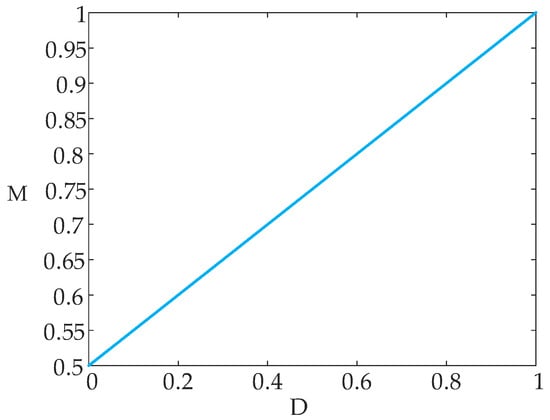
Figure 4.
Voltage gain curve.
3.2. Soft-Switching Analysis
As Figure 2 shows, the current i1 flowing through switches S3 and S4 has dropped to zero before they turn on or off. Therefore, S3 and S4 can achieve ZCS turn-on and turn-off. To achieve ZVS for switches S1 and S2, S1 and S2 must complete the charging and discharging of their parasitic capacitance within the dead time. This requires the energy stored in inductor L1 to exceed the energy in the parasitic capacitance of the switches. Based on the topology structure, the ZVS condition of the switches S1 and S2 can be expressed as follows:
where IL1_off represents the current in inductor L1 when the switches turn off and Cj denotes the value of the parasitic capacitance. Based on the equation, the ZVS conditions of S1 and S2 can be derived as follows:
The average current flowing through inductor L1 equals the negative of the average current flowing through switch S4, which can be shown as follows:
Then, IL1_off can be calculated as follows:
3.3. Pseudo Partial Power Analysis
For the converter described above, a portion of the power is handled by the auxiliary inductor L1 and auxiliary capacitor C2. The calculation of the power is calculated as follows:
Based on Equations (11) and (15), the partial power transferred can be derived as follows:
Then, the ratio of the partial power P transferred by auxiliary inductor L2 and auxiliary capacitor C4 to the total power Po can be calculated as follows:
The proportional diagram of partial power is shown in Figure 5.
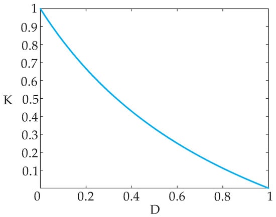
Figure 5.
Proportional of the transferred partial power.
From the above equation, it can be seen that K decreases as the duty cycle D increases. Theoretically, when D approaches zero, K will reach its maximum value of 1.
4. Converters Parameter Design of the Converter
To verify the analysis of the converter, a prototype will be built, and the parameter design of the converter is shown as follows.
The ratio of the transformer can be designed based on the relationship between the input voltage and the output voltage. When the converter operates at a low duty cycle, it generates significant spike resonant currents. Therefore, in practical applications, the voltage gain of the converter must be less than unity. Then, the ratio n of the transformer can be derived according to the following equation.
Vin_min denotes the minimum value of the input voltage and Vin_max denotes the maximum value of the input voltage.
The design of the resonant tank requires that the minimum conduction time of the switches exceed half a resonant cycle to enable the converter to operate in current discontinuous mode. Then, the resonant frequency can be expressed as follows:
where Dmin represents the minimum duty cycle of the switches, and can be calculated as follows:
The value of resonant capacitor C4 can be designed based on the current discontinuity conditions. To satisfy the discontinuity of the primary side current, resonant capacitor C4 must meet condition, shown as follows:
According to Equation (1), the value of resonant inductor L2 can be calculated as follows:
Based on Equations (18), (20) and (21), the range of L2 can be calculated as follows:
5. Simulation Analysis and Experimental Validation
To verify the correctness of the above theoretical analysis, a simulation model was first built in the software for validation. In a closed-loop situation, the voltage and current waveforms on capacitor C2 are shown in Figure 6.
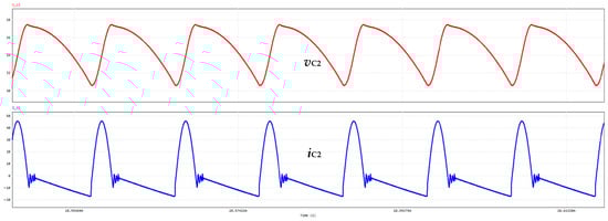
Figure 6.
Voltage and current waveforms of capacitor C2.
This is the current and voltage waveform across capacitor C2 under steady-state conditions. When the system enters a steady state, the duty cycle D is constant, the capacitor voltage fluctuates around a certain value, and the capacitor current iC2 charges and discharges capacitor C2 within a cycle as the switch changes, generally showing a periodic pattern.
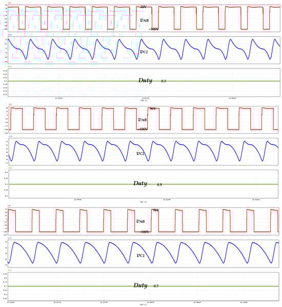
Figure 7.
Waveform diagram of voltage VAB between AB ports and voltage VC2 across capacitor C2 under different duty cycles D.
From the simulation results in Figure 7, it can be seen that when the duty cycle D increases, the voltage across the auxiliary capacitor C2 decreases, and the voltage across the input terminals AB is VAB = Vin − VC2, so the voltage across AB increases. The simulation results are consistent with the theoretical analysis, confirming the correctness of the theoretical analysis.
When the input voltage is 100 V, adjust the duty cycle D to obtain the average capacitor voltage VC2 under any duty cycle D. Plot the relationship between the capacitor voltage VC2 and the duty cycle D as a line chart; the relevant graph is shown in Figure 8.
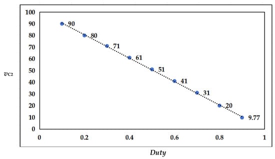
Figure 8.
The relationship curve between capacitor voltage VC2 and duty cycle D.
As shown in Figure 8, as the duty cycle D increases, the voltage across capacitor C2 decreases. And the relationship between the capacitor voltage and the duty cycle as specified in Equation (11) is satisfied among them.
The input current i1 and the auxiliary inductor current iL1 waveforms are shown in Figure 9.
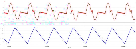
Figure 9.
Input current and auxiliary inductor current.
As can be seen from Figure 9, the waveform on inductor L1 is a periodically varying triangular wave, while the input waveform i1 is similar to a sine wave.
To validate the feasibility of the proposed converter topology and the validity of the theoretical analysis, an experimental prototype was designed based on the parameter design. This prototype operates with an input voltage range of 100 V to 125 V, an output voltage of 400 V, a working frequency of 100 kHz, and a maximum output power of 1000 W. The prototype is shown in Figure 10. The parameters of the prototype are listed in Table 1. Based on Equation (3) and the prototype′s relevant parameters, the value of resonant inductor L2 should be less than 116 uH. The leakage inductance of the transformer used in the experiment is 8 uH, which meets the requirement. Therefore, the internal leakage inductance of the transformer is treated as the resonant inductor, so the value of resonant inductance L2 is 8 uH. According to Equations (18) and (21), the value of the resonant capacitor is calculated to be 150 nF. The specific parameter design is shown in Table 1.
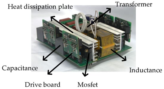
Figure 10.
Experimental prototype.

Table 1.
Transformer Prototype Parameters.
Figure 11 shows the full-load steady-state operating waveforms of the converter under different input voltages. As seen, voltage vgs1 represents the driver signal voltage of S1. During the actual experiment, diodes D1~D4 were replaced with MOSFET to achieve synchronous rectification. And vgs_SR is the driving signal of the synchronous rectifier. Current i2 represents the secondary side current of the converter, while voltage Vout indicates the output voltage. As shown in Figure 10, the converter operates in current discontinuous mode, enabling ZCS for switching devices S3 and S4. At the same time, the current i2 in Figure 11 is the same as the current i1 in the simulation, verifying the accuracy of the simulation.
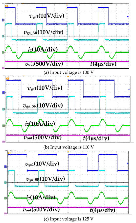
Figure 11.
Full-load steady-state waveforms under different input voltages.
Figure 12 shows the ZVS waveforms of the converter under different input voltages. As seen, vgs2 represents the driver voltage of switch S2, vds2 denotes the drain source voltage of switch S2, vAB indicates the voltage between bridge arm midpoints A and B, and iL1 signifies the current through auxiliary inductor L1. This current is approximately the same as the current iL1 in the simulation, further demonstrating the correctness of the related theory in the paper. As illustrated in Figure 12, ZVS is achieved for switch S2 regardless of the input voltage applied.
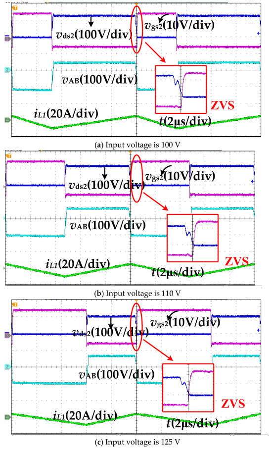
Figure 12.
Zero-voltage waveforms under different input voltages.
At the same time, it can be seen from Figure 12 that when the positive–negative ratio of the input voltage changes (i.e., when the duty cycle D changes), it can be known from Equation (11) that the voltage across capacitor C2 will also change, which in turn causes a change in the voltage VAB at the input port AB.
Figure 13 shows the dynamic waveforms of the converter during the load change from a light load to a full load under different input voltages. As seen, iout represents the output current. As shown in Figure 12, the converter maintains normal closed-loop operation during the load change. Additionally, the closed-loop dynamic adjustment time is almost the same under different input voltages.
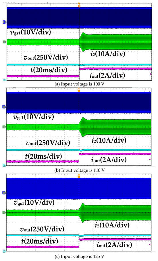
Figure 13.
Dynamic waveforms of load change from light load to full load.
Figure 14 shows the dynamic waveform when the input voltage Vin changes. As seen, the output voltage remains stable despite variations in the input voltage. This demonstrates the excellent dynamic response of the converter.
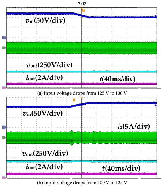
Figure 14.
Dynamic waveform when input voltage changes.
Figure 15 shows the efficiency comparison curves of the converter under different input voltages and output power. At a light load, conduction loss is relatively small, but switching loss (soft-switching effect weakened) and fixed loss account for a significant proportion, total loss decreases slowly, and efficiency drops. At a full load, conduction loss becomes the dominant loss and rises rapidly with increasing power; although switching loss is still relatively low, it cannot compensate for the increase in conduction loss, leading to a decline in efficiency. At a medium load (around 460 W), switching loss is minimized due to sufficient soft switching, the increase in conduction loss with current has not yet offset the advantage of low switching loss, core loss is also at a low level, various losses reach an optimal balance, and overall efficiency is at its highest. At approximately 460 W, the converter achieves peak efficiency of about 95%, and its full-load efficiency is around 93%.
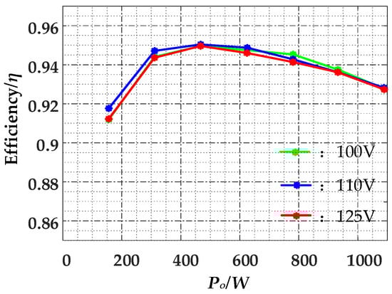
Figure 15.
Efficiency curves of the converter at different input voltages and power levels.
6. Comparison with Other Topologies
To highlight the relevant characteristics of the transformer proposed in this paper, it was compared with the transformers cited in the references mentioned in the abstract, and the results of the comparison are shown in Table 2.
Table 2.
Comparative analysis of related topological properties.
As can be seen from Table 2, the switch-multiplexed resonant converter proposed in this paper has fewer components compared to Wu′s [21] bidirectional current-source soft-switching series-resonant converter, Zuo′s [22] fixed-frequency dual-PWM interleaved boost LLC resonant converter, and Gu′s [23] reconfigurable current-source LLC resonant converter, with only three magnetic elemnts, lower energy loss (soft switching eliminates switching loss; DCM reduces reverse recovery loss and reactive current), higher power density, more compact size, and overall better performance.
7. Conclusions
This paper proposes a novel switch-multiplexed resonant converter and details its operating principles. By adjusting the duty cycle of the multiplexed switches, the partial power transferred through the auxiliary inductor can be controlled. Thus, the total power transferred by the converter can be adjusted to regulate the output voltage. This paper analyzes the voltage gain, soft-switching characteristics, and conditions for resonant current discontinuity of the converter, while providing specific design schemes for the parameters. Finally, a 1000 W experimental prototype was designed and validated through testing, confirming the feasibility of the proposed converter topology and conclusions.
Author Contributions
Methodology, Z.Y.; validation, Y.Z. (Yizhan Zhuang); investigation, Y.Z. (Yiming Zhang); writing—original draft, X.C. All authors have read and agreed to the published version of the manuscript.
Funding
This research was funded by the National Natural Science Foundation of China under grant number 52407197.
Data Availability Statement
The original contributions presented in this study are included in the article. Further inquiries can be directed to the corresponding author.
Conflicts of Interest
The authors declare no conflicts of interest.
References
- Bokolo, A.J. Enabling Intelligent Internet of Energy-Based Provenance and Green Electric Vehicle Charging in Energy Communities. Energies 2025, 18, 4827. [Google Scholar] [CrossRef]
- Jarnut, M.; Kaniewski, J.; Buciakowski, M. Energy Storage Systems for Fluctuating Energy Sources and Fluctuating Loads—Analysis of Selected Cases. Energies 2025, 18, 4792. [Google Scholar] [CrossRef]
- He, P.; Chen, Q.; Chen, L. The Impact of ESG on Corporate Value Under the ‘Dual Carbon’ Goals: Empirical Evidence from Chinese Energy Listed Companies. Energies 2025, 18, 4811. [Google Scholar] [CrossRef]
- Palanidoss, S.; Vishnu, T.V.S. Experimental analysis of conventional buck and boost converter with integrated dual output converter. In Proceedings of the 2017 International Conference on Electrical, Electronics, Communication, Computer, and Optimization Techniques (ICEECCOT), Mysuru, India, 15–16 December 2017; pp. 323–329. [Google Scholar]
- Mousa, M.; Ahmed, M.; Orabi, M. A switched inductor multilevel boost converter. In Proceedings of the 2010 IEEE International Conference on Power and Energy, Kuala Lumpur, Malaysia, 29 November–1 December 2010; pp. 819–823. [Google Scholar]
- Hwu, K.I.; Tau, Y.T. A Forward Converter Having an FPGA-based PID Controller with Parameters On-ine Tuned. In Proceedings of the 2005 International Conference on Power Electronics and Drives Systems, Kuala Lumpur, Malaysia, 28 November–1 December 2005; pp. 1239–1243. [Google Scholar]
- de Campos, A.S.C.; Gomes, A.C.; de Morais, A.S. Multi-winding bidirectional flyback converter. In Proceedings of the 2017 Brazilian Power Electronics Conference (COBEP), Juiz de Fora, Brazil, 19–22 November 2017; pp. 1–6. [Google Scholar]
- Cao, J.; Zhang, X.; Rao, P.; Zhou, S.; Zhou, F.; Zhang, Q. Design of Three-Phase Delta-Delta LLC Resonant Converter. In Proceedings of the 2020 IEEE Vehicle Power and Propulsion Conference (VPPC), Gijon, Spain, 18 November–16 December 2020; pp. 1–5. [Google Scholar]
- Xu, D.; Zhou, G.; Huang, R.; Liu, X.; Liu, F. High efficiency half bridge class-D audio amplifier system with front-end symmetric bipolar outputs LLC converter. IEEE Trans. Ind. Electron. 2021, 68, 1220–1230. [Google Scholar] [CrossRef]
- Tan, D.F.D. A review of immediate bus architecture: A system perspective. IEEE J. Emerg. Sel. Topics Power Electron. 2014, 2, 363–373. [Google Scholar] [CrossRef]
- Lim, S.; Ranson, J.; Otten, D.M.; Perreault, D.J. Two-stage power conversion architecture suitable for wide range input voltage. IEEE Trans. Power Electron. 2015, 30, 805–816. [Google Scholar] [CrossRef]
- Ahmed, M.H.; Chao, F.; Lee, F.C.; Li, Q. Single-stage high-efficiency 48/1 V sigma converter with integrated magnetics. IEEE Trans. Ind. Electron. 2020, 67, 192–202. [Google Scholar] [CrossRef]
- Chen, H.; Wu, X. LLC resonant DC transformer (DCX) with parallel PWM output tight regulation. In Proceedings of the 2014 IEEE Energy Conversion Congress and Exposition (ECCE), Pittsburgh, PA, USA, 14–18 September 2014; pp. 4742–4747. [Google Scholar]
- Liu, T.; Wu, X.; Yang, S. 1 MHz 48–12V regulated DCX with single transformer. IEEE J. Emerg. Sel. Top. Power Electron. 2021, 9, 38–47. [Google Scholar] [CrossRef]
- Gu, R.; Duan, J.; Zhang, D.; Liu, H. Regulated series hybrid converter with DC transformer (DCX) for step-up power conversion. IEEE Trans. Ind. Electron. 2022, 69, 8961–8971. [Google Scholar] [CrossRef]
- Sun, J.; Xu, M.; Reusch, D.; Lee, F.C. High efficiency quasi-parallel voltage regulators. In Proceedings of the 2008 Twenty-Third Annual IEEE Applied Power Electronics Conference and Exposition, Austin, TX, USA, 24–28 February 2008; pp. 811–8174. [Google Scholar]
- Zhu, H.; Hu, B.; Xie, X.; Zhang, C.; Dong, R.; Wang, J. LLC resonant converter with partial-power auxiliary DC/DC module for wide-range output applications. In Proceedings of the 2022 IEEE 3rd China International Youth Conference on Electrical Engineering (CIYCEE), Wuhan, China, 3–5 November 2022; pp. 1–7. [Google Scholar]
- Li, L.; Qian, Y.; Yu, L.; Xu, S.; Sun, W. Modelling of quasi-parallel Sigma DC-DC converter for high efficiency single-stage voltage regulator. In Proceedings of the 2022 IEEE Applied Power Electronics Conference and Exposition (APEC), Houston, TX, USA, 20–24 March 2022; pp. 01–05. [Google Scholar]
- Lu, Z.; Xu, G.; Xiong, W.; Sun, Y.; Su, M. A quasi-two-stage isolated bidirectional buck-DAB converter for wide input voltage range. IEEE Trans. Power Electron. 2023, 38, 1384–1390. [Google Scholar] [CrossRef]
- Lu, Z.; Su, M.; Xu, G.; Li, L.; Xiong, W.; Fang, J. Switchmultiplexed quasi-two-stage isolated bidirectional buck-DAB converter with full load ZVS range. IEEE Trans. Power Electron. 2023, 38, 10541–10546. [Google Scholar] [CrossRef]
- Wu, H.; Sun, K.; Li, Y.; Xing, Y. Fixed-frequency PWM-controlled bidirectional current-fed soft-switching series-resonant converter for energy storage applications. IEEE Trans. Ind. Electron. 2017, 64, 6190–6201. [Google Scholar] [CrossRef]
- Zuo, Y.; Shen, X.; Du, B.; Cobaleda, D.B.; Wouters, H.; Martinez, W. Fixed-frequency dual PWM interleaved boost LLC resonant converter for a wide input voltage for photovoltaic applications. In Proceedings of the 2024 IEEE 10th International Power Electronics and Motion Control Conference (IPEMC2024-ECCE Asia), Chengdu, China, 17–20 May 2024; pp. 4172–4177. [Google Scholar] [CrossRef]
- Gu, R.; Zhang, D.; Duan, J.; Zhang, W.; Li, A. A reconfigurable current-fed LLC resonant converter with circulant PWM control and wide gain range. IEEE Trans. Ind. Electron. 2025, 72, 3575–3586. [Google Scholar] [CrossRef]
Disclaimer/Publisher’s Note: The statements, opinions and data contained in all publications are solely those of the individual author(s) and contributor(s) and not of MDPI and/or the editor(s). MDPI and/or the editor(s) disclaim responsibility for any injury to people or property resulting from any ideas, methods, instructions or products referred to in the content. |
© 2025 by the authors. Licensee MDPI, Basel, Switzerland. This article is an open access article distributed under the terms and conditions of the Creative Commons Attribution (CC BY) license (https://creativecommons.org/licenses/by/4.0/).