Article

A Switched-Capacitor-Based Quasi-H7 Inverter for Common-Mode Voltage Reduction

by
Thi-Thanh Nga Nguyen
1,
Tan-Tai Tran
2,
Minh-Duc Ngo
1,* and
Seon-Ju Ahn
3,*
1
Department of Automation, Thai Nguyen University of Technology (TNUT), 666, 3/2 Street, Tich Luong Ward, Thai Nguyen City 24132, Vietnam
2
Faculty of Electrical Engineering Technology, Industrial University of Ho Chi Minh City, Ho Chi Minh City 71700, Vietnam
3
Department of Electrical Engineering, Chonnam National University, Buk-gu, Gwangju 61186, Republic of Korea
*
Authors to whom correspondence should be addressed.
Energies 2025, 18(12), 3218; https://doi.org/10.3390/en18123218
Submission received: 12 May 2025 / Revised: 14 June 2025 / Accepted: 17 June 2025 / Published: 19 June 2025

Abstract

:
This paper proposes a novel three-phase two-level DC-AC inverter with significantly reduced common-mode voltage. The proposed inverter combines a conventional three-phase H7 configuration with a voltage multiplier network, effectively doubling the DC-link voltage relative to the input. Compared to existing solutions, the topology achieves a remarkably low common-mode voltage, limited to only 16.6% of the DC-link voltage. Additionally, the voltage stress across the additional switches remains at half of the DC-link voltage. The paper details the operating principles, mathematical formulation, and circuit-level analysis of the proposed inverter. Simulation results are provided to validate its performance. Furthermore, a hardware prototype has been implemented using a DSP TMS320F28379D microcontroller manufactured by Texas Instruments, headquartered in Dallas, TX, USA in conjunction with an Altera Cyclone® IV EP4CE22F17C6N FPGA-based digital control platform manufactured by Intel Corporation, headquarters in Santa Clara, CA, USA. Experimental results are presented to confirm the effectiveness and feasibility of the proposed design.

1. Introduction

Common-mode voltage (CMV) plays a crucial role in various applications, particularly in transformerless photovoltaic (PV) and electric motor drives [1,2,3,4,5]. In conventional pulse-width modulation (PWM) inverters, CMV with high frequency and amplitude is known to cause several undesirable effects, including electromagnetic interference (EMI), ground leakage currents, and bearing current generation [6,7]. In a typical three-phase system, the CMV is calculated as the average of the voltages between nodes A-O, B-O, and C-O and is expressed as:
V C M = ( V A O + V B O + V C O ) 3 .
where the point “O” represents the negative terminal of the input DC source, and VAO, VBO, and VCO denote the phase voltages measured with respect to this point, as illustrated in Figure 1.
To address the CMV issues associated with conventional PWM inverters, a lot of reduction techniques have been proposed in previous studies. These approaches include modifications to inverter topologies as well as the development of advanced PWM control strategies.
Improved modulation control strategies, such as Active Zero State PWM (AZSPWM), Near State PWM (NSPWM), and Reduced Switching PWM (RSPWM), have been proposed to mitigate CMV variation by avoiding the use of zero-voltage states [8,9]. These techniques reduce the magnitude of the CMV to approximately 33.3% of the input DC voltage. However, this improvement comes at the cost of degraded power quality, a reduced modulation index, and lower efficiency, ultimately affecting overall inverter performance. To further reduce the CMV, hybrid space vector PWM (SVPWM) methods have been explored in [10]. The voltage linearity characteristics of these strategies are similar to those of the AZSPWM method. In addition, the CMV frequency was only equal to three times the fundamental frequency. Nevertheless, hybrid SVPWM techniques present challenges such as increased algorithmic complexity and higher switching losses. A novel model predictive control method is proposed in [11] to suppress common-mode voltage by strategically limiting the number of usable voltage vectors within each sector. As a result, the CMV magnitude is effectively constrained to 33.3% of the input DC voltage. In parallel, [12] introduces a low-common-mode SVPWM technique that divides the voltage plane into 12 sectors, achieving the same CMV magnitude while tripling the CMV switching frequency.
In addition to modulation strategies, various inverter topologies have been proposed to reduce the CMV. As discussed in [13,14,15], three-phase four-leg inverter structures are commonly employed for CMV suppression. In [13], a near state vector selection-based model for predictive control is introduced to limit the common-mode voltage by using a minimum number of usable vectors in every switching period. This method reduces the magnitude of the CMV to approximately 25% of the input DC voltage. In [14,15], the fourth leg of a three-phase four-leg inverter is actively controlled to compensate for CMV variation, effectively achieving zero common-mode voltage. A three-phase H7 inverter was introduced in [16], in which an additional switch is inserted between the input DC source and the conventional H-bridge inverter. A schematic of the conventional three-phase H7 inverter is shown in Figure 1. By controlling this additional switch to float the inverter from the DC source during zero states, the CMV varies between Vdc/3 and Vdc, as summarized in Table 1. A voltage-clamping H8 topology, discussed in [17], employs two additional active switches to disconnect the power source from the inverter during freewheeling states. This configuration maintains a constant CMV during mode transitions, with the CMV magnitude limited to only 33.3% of the input DC voltage. Alternative H8 topologies were also presented in [18,19], utilizing only two extra switches to constrain CMV variation. In these designs, the CMV fluctuation is similarly restricted to 33.3% of the input DC voltage.
In this paper, a novel switched-capacitor-based quasi-H7 inverter (SC-qH7 inverter) is proposed. The presented topology combines a conventional three-phase H7 inverter with a voltage multiplier network. Unlike existing solutions, the CMV of the proposed inverter varies only from VPN/6 to VPN/3, whereas the CMV in the conventional H7 inverter topology fluctuates from VPN/3 to VPN. Furthermore, the SC-qH7 inverter supports the full modulation index range without compromising on performance. A switched-capacitor network is proposed to achieve low common-mode voltage and voltage boosting in the proposed SC-qH7 inverter. Similar to conventional switched-capacitor circuits, the proposed SC-qH7 inverter also introduces an impulse charging current in capacitors. This issue of current waveforms can be efficiently mitigated by adding resonant inductors in the switched capacitor loop as presented in [20,21]. The proposed inverter structure is introduced in Section 2, followed by a description of the applied PWM control technique in Section 3. Simulation and experimental validation results are provided in Section 4.

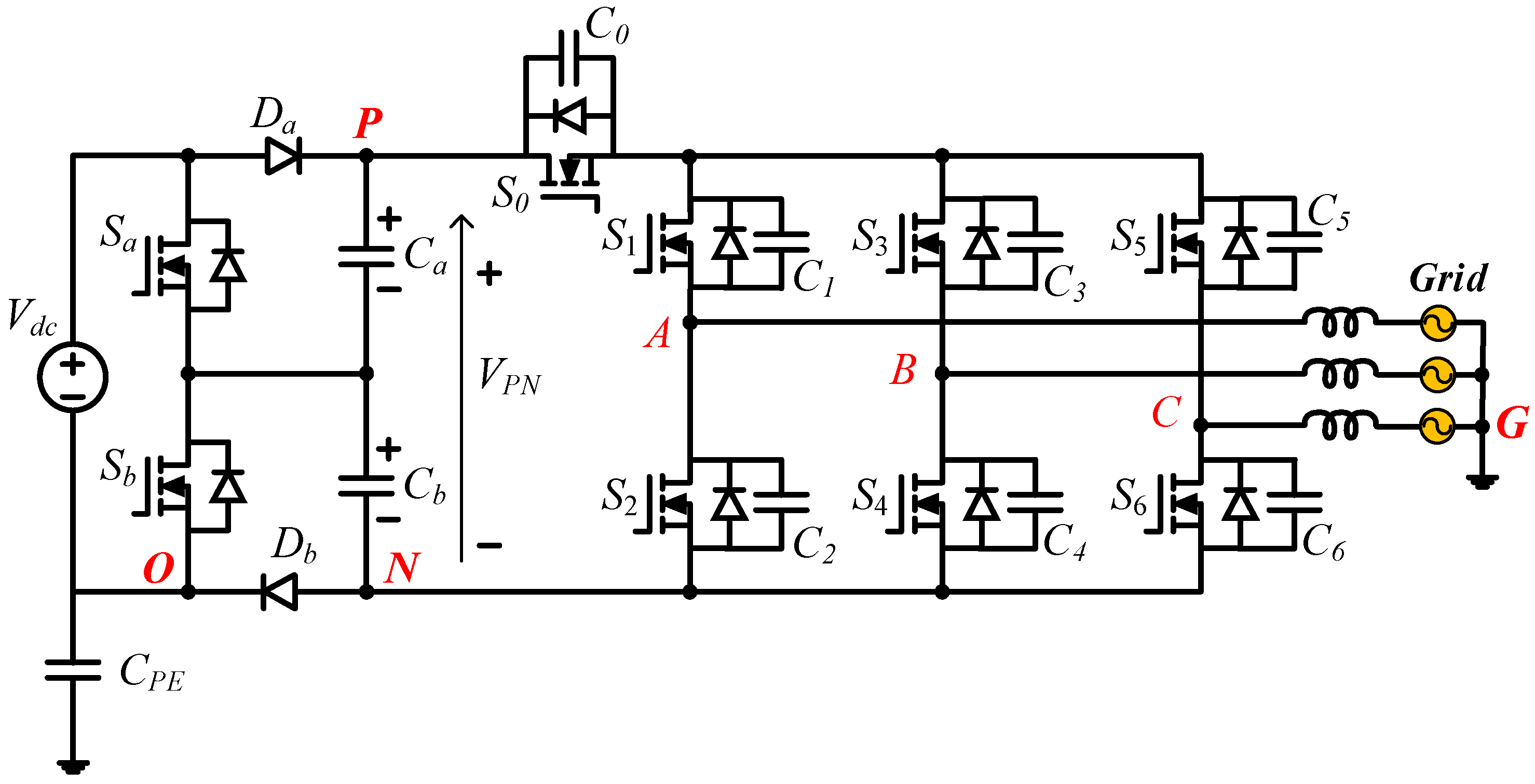
2. Topology and Operating Principle of the SC-qH7 Inverter

Figure 2 illustrates the circuit configuration of the proposed SC-qH7 inverter. In this topology, a switched-capacitor network is added to the conventional H7 inverter.
From Figure 2, the voltage across diode Db (VNO) is calculated as follows:
V N O = V C b S b   is   on 0 S b   is   off  
The CMV (VCM) of the proposed SC-qH7 inverter can be rewritten as follows:
V C M = V N O + ( V A N + V B N + V C N ) 3  

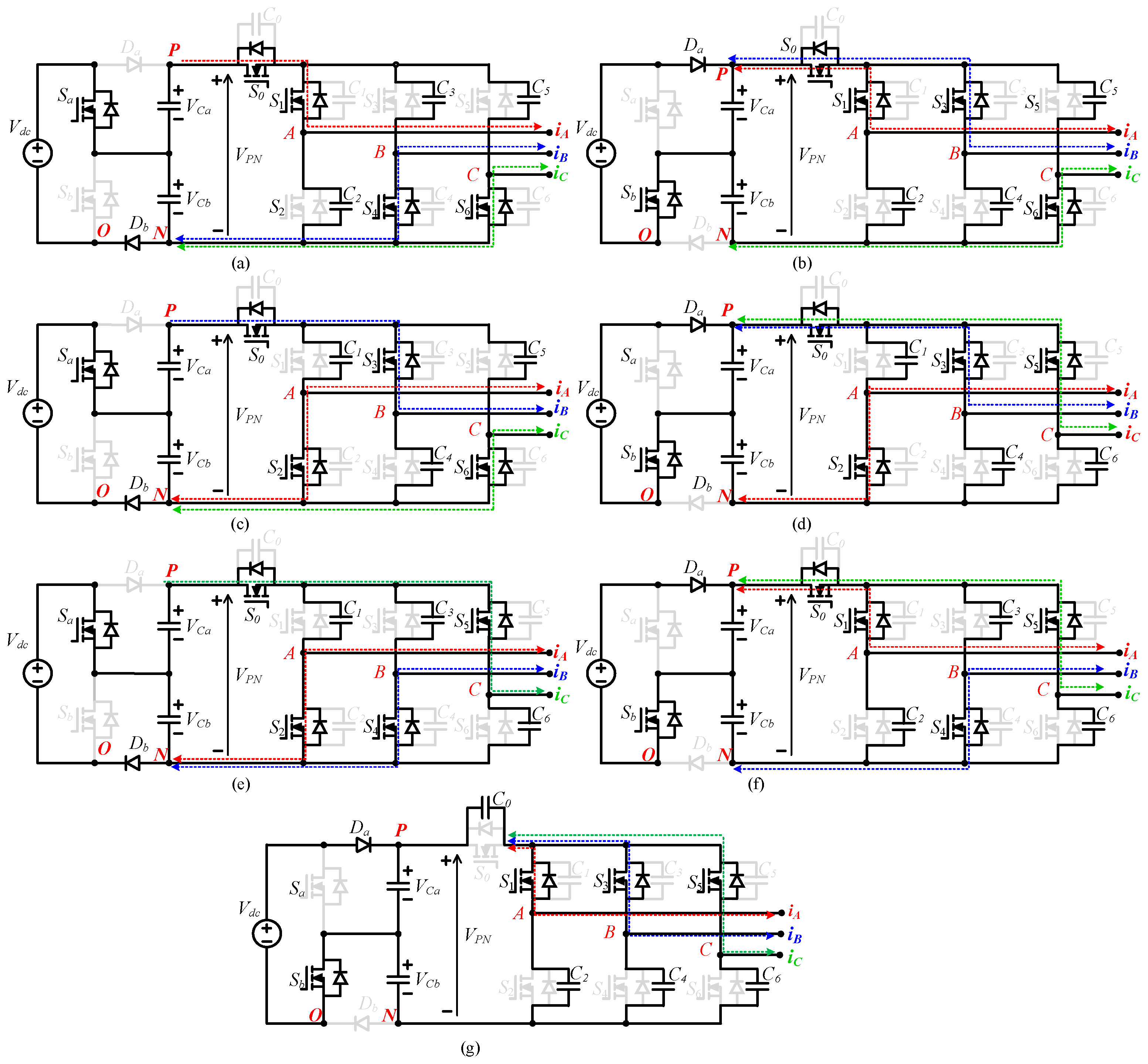
2.1. Operating Principle of Proposed SC-qH7 Inverter

The operating principles of the proposed SC-qH7 inverter can be explained through its distinct switching modes, as summarized in Table 2. Similar to the conventional H7 inverter [15], the proposed SC-qH7 inverter has seven switching modes, as shown in Figure 3.
Mode 1 (see Figure 3a): five switches Sa, S0, S1, S4, and S6 are turned on, while four switches Sb, S2, S3, and S5 are turned off. As a result, the voltages between the nodes A-N, B-N, and C-N of the proposed SC-qH7 inverter are VPN, 0 V, and 0 V, respectively. During this mode, diode Da is blocked, whereas diode Db is forward-based. Consequently, capacitor Ca discharges, and capacitor Cb charges through the loop Vdc-Sa-Cb-Db. The corresponding CMV during this mode is VPN/3.
Mode 2 (see Figure 3b): five switches Sb, S0, S1, S3, and S6 are turned on, while four switches Sa, S2, S4, and S5 are turned off. As a result, the voltages between the nodes A-N, B-N, and C-N are VPN, VPN, and 0 V, respectively. During this mode, diode Db is blocked, and diode Da is forward-based. Capacitor Cb discharges, while capacitor Ca charges through the loop Vdc-Da-Ca-Sb. The corresponding CMV during this mode is VPN/6.
Mode 3 (see Figure 3c): five switches Sa, S0, S2, S3, and S6 are turned on, while four switches Sb, S1, S4, and S5 are turned off. As a result, the voltages between the nodes A-N, B-N, and C-N are 0 V, VPN, and 0 V, respectively. During mode 3, diode Da is blocked, while diode Db is forward-based. Capacitor Ca discharges, and capacitor Cb charges through the loop Vdc-Sa-Cb-Db. The corresponding CMV during this mode is VPN/3.
Mode 4 (see Figure 3d): switches Sb, S0, S2, S3, and S5 are turned on, while four switches Sa, S1, S4, and S6 are turned off. As a result, the voltages between the nodes A-N, B-N, and C-N are 0 V, VPN, and VPN, respectively. During mode 4, diode Db is blocked, while diode Da is forward-based. Capacitor Cb discharges, and capacitor Ca charges through the loop Vdc-Da -Ca -Sb. The corresponding CMV during this mode is VPN/6.
Mode 5 (see Figure 3e): switches Sa, S0, S2, S4, and S5 are turned on, while four switches Sb, S1, S3, and S6 are turned off. As a result, the voltages between the nodes A-N, B-N, and C-N are 0 V, 0 V, and VPN, respectively. During this mode, diode Da is blocked, while diode Db is forward-based. Capacitor Ca discharges, and capacitor Cb charges through the loop Vdc-Sa-Cb-Db. The corresponding CMV during this mode is VPN/3.
Mode 6 (see Figure 3f): switches Sb, S0, S1, S4, and S5 are turned on, while four switches Sa, S2, S3, and S6 are turned off. As a result, the voltages between the nodes A-N, B-N, and C-N are VPN, 0 V, and VPN, respectively. During mode 6, diode Db is blocked, while diode Da is forward-based. Capacitor Cb discharges, and capacitor Ca charges through the loop Vdc-Da-Ca-Sb. The corresponding CMV during this mode is VPN/6.
Mode 7 (see Figure 3g): four switches Sb, S1, S3, and S5 are turned on, while five switches Sa, S0, S2, S4, and S6 are turned off. During this mode, diode Db is blocked, while diode Da is forward-based. Capacitor Cb discharges, and capacitor Ca charges through the loop Vdc-Da-Ca-Sb.
As shown in Figure 2, the DC-link voltage of the proposed SC-qH7 inverter is:
V P N = V C a + V C b = 2 V d c .
For the same input DC voltage, the proposed SC-qH7 inverter achieves a DC-link voltage that is twice that of the conventional H7 inverter. Based on the operating principles described earlier, it is observed that the CMV of the SC-qH7 inverter varies from VPN/6 to VPN/3 (approximately 16.6% of VPN) during powering modes (modes 1 through 6). Notably, during these modes, switch S0 remains in the ON state, contributing to stable power delivery. When the inverter transitions to mode 7, switch S0 is turned OFF. Unlike the conventional H7 topology, the proposed topology incorporates seven additional capacitors positioned alongside switches S0 through S6, as shown in Figure 2. These capacitors, together with the inherent junction capacitances of the switches, form a coupling path between the input DC source and the inverter’s AC output side. Consequently, under the zero-state condition, the CMV is primarily determined by the combined effect of these capacitive elements.

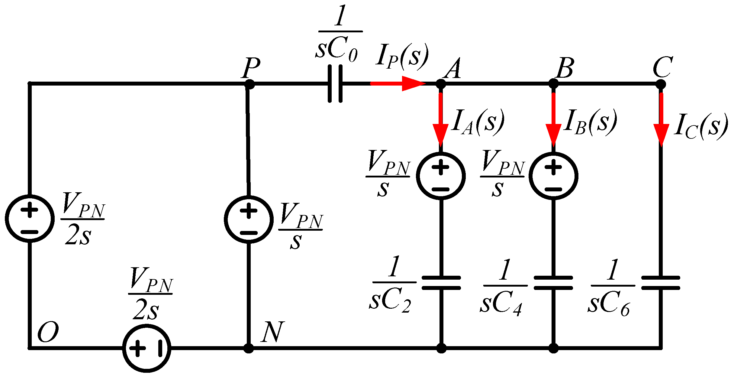
2.2. Capacitor Model During Freewheeling Mode

The transition process from the powering mode to the freewheeling mode is analyzed in this section, with a specific focus on the mode transition from mode 2 to mode 7. The transitions from mode 4 and mode 6 follow a similar process and are therefore omitted for brevity. At the initial time, it is assumed that the system is operating in mode 2, as illustrated in Figure 3b. The initial conditions are formulated as follows:
V C 0 = 0 V V C 2 = V P N V C 4 = V P N V C 6 = 0 V  
The frequency-domain equivalent of the proposed SC-qH7 inverter is depicted in Figure 4, where the initial conditions of the system are represented by equivalent voltage sources. From Figure 4, the following mathematical equations are obtained:
I P s = I A s + I B s + I C s I P s s C 0 + I A s s C 2 = 0 I A s s C 2 I B s s C 4 = 0 I C s s C 6 I B s s C 4 = V P N s
With the frequency-domain equivalents, the CMV of the proposed SC-qH7 inverter (VCM(s)) when entering mode 7 is expressed as:
V C M s = V P N 2 s + 1 3 V P N s + I A ( s ) s C 2 + V P N s + I B ( s ) s C 4 + I C ( s ) s C 6
By solving Equations (2) and (3), the CMV of the proposed SC-qH7 inverter (VCM(s)) when entering mode 7 can be rewritten as:
V C M V s = C 0 + C 2 + C 4 C 6 C 0 + C 2 + C 4 + C 6 V P N 2 s  
Taking the inverse Laplace transform, we get:
V C M V = C 0 + C 2 + C 4 C 6 C 0 + C 2 + C 4 + C 6 V P N 2  
When C0 = C2 = C4 = C6, the VCMV under mode 7 is equal to VPN/4.
Therefore, the CMV of the proposed SC-qH7 inverter only takes values of VPN/3, VPN/6, or VPN/4. All the switching modes and the corresponding CMV of the proposed SC-qH7 inverter are given in Table 2. As highlighted in the table, the variation range of the CMV in the proposed topology is limited to just 16.6% of the DC-link voltage, representing a significant improvement compared to conventional inverter structures.

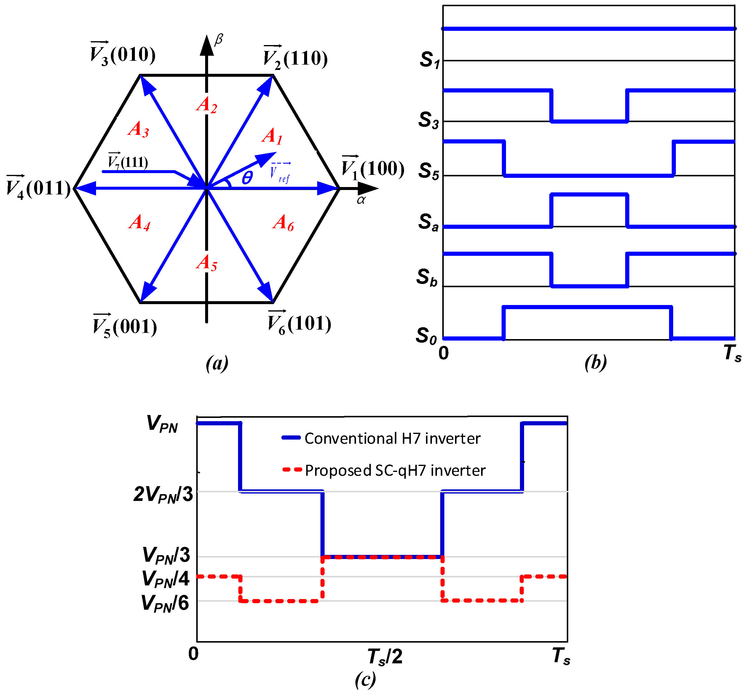
3. PWM Control Technique of SC-qH7 Inverter

Figure 5 illustrates the proposed PWM control strategy for the SC-qH7 inverter. Similar to the Discontinuous PWM (DPWM) technique, the proposed method utilizes three types of switching vectors: an odd active vector, an even active vector, and the zero vector V7. If the final reference voltage is located in sector A1, as presented in Figure 5a, the switching sequence will be (111)-(110)-(100)-(100)-(110)-(111). The complete switching pattern for each sector under the DPWM strategy for the SC-qH7 inverter is summarized in Table 3. The time durations of the voltage space vectors V 1 , V 2 , V 3 , V 4 , V 5 , V 6 , and V 7 during a switching period are denoted as T1, T2, T3, T4, T5, T6, and T7, respectively.
In sector A1, as illustrated in Figure 5 and Table 3, the reference voltage vector ( V r e f ) is synthesized using the three vectors: V 1 , V 2 , and V 7 . Based on the volt–second balance principle, we derive the following:
T s × V r e f   = T 1 × V 1 + T 2 × V 2 + T 7 × V 7
where Ts is the switching period.
The time durations of the voltage space vectors V 1 , V 2 , and V 7 can be calculated as:
T 1 = M i × T s × sin π 3 θ         T 2 = M i × T s × sin θ                 T 7 = T s T 1 T 2                        
In the above equations, M i = 3 V m V P N represents the modulation index, where Vm is the magnitude of the reference voltage vector and VPN is the DC-link voltage.
Similarly, in sector A2, the reference voltage vector ( V r e f ) is synthesized using the three vectors V 2 , V 3 , and V 7 . The time durations of the voltage space vectors V 2 , V 3 , and V 7 can be calculated as:
T 2 = M i × T s × sin θ + π 3         T 3 =   M i × T s × sin θ π 3         T 7 =   T s T 2 T 3                        
Similarly, in sector A3, the reference voltage vector ( V r e f ) is synthesized using the three vectors V 3 , V 4 , and V 7 . The time durations of the voltage space vectors V 3 , V 4 , and V 7 can be calculated as:
T 3 = M i × T s × sin θ                   T 4 = M i × T s × sin θ 2 π 3         T 7 = T s T 3 T 4                        
Similarly, in sector A4, the reference voltage vector ( V r e f ) is synthesized using the three vectors V 4 , V 5 , and V 7 . The time durations of the voltage space vectors V 4 , V 5 , and V 7 can be calculated as:
T 4 = M i × T s × sin θ π 3         T 5 = M i × T s × sin θ π         T 7 = T s T 4 T 5                        
Similarly, in sector A5, the reference voltage vector ( V r e f ) is synthesized using the three vectors V 5 , V 6 , and V 7 . The time durations of the voltage space vectors V 5 , V 6 , and V 7 can be calculated as:
T 5 = M i × T s × sin θ 2 π 3       T 6 = M i × T s × sin θ + 2 π 3         T 7 = T s T 5 T 6                        
Similarly, in sector A6, the reference voltage vector ( V r e f ) is synthesized using the three vectors V 1 , V 6 , and V 7 . The time durations of the voltage space vectors V 1 , V 6 , and V 7 can be calculated as:
T 1 = M i × T s × sin θ + π 3         T 6 = M i × T s × sin θ π         T 7 = T s T 1 T 6                        
The proposed SC-qH7 inverter under the proposed PWM control strategy offers the notable advantage of maintaining linear operation across the full range of the modulation index. A comparison of the CMV between the conventional H7 inverter and the proposed SC-qH7 inverter under the DPWM strategy in sector A1 is also presented in Figure 5c. As shown in Figure 5b, during even active vectors and the zero vector V7, switch Sa remains in the OFF state while switch Sb remains ON. Conversely, during odd active vectors, switch Sa is ON and switch Sb is OFF. Additionally, switch S0 remains ON throughout the operation, except during vector V7, where it is turned OFF. This switching scheme ensures that the CMV of proposed SC-qH7 inverter only takes values of VPN/3, VPN/4, or VPN/6. As a result, the proposed SC-qH7 inverter retains all the inherent advantages of voltage source inverters (VSIs) operated under DPWM, such as reduced switching losses, low total harmonic distortion (THD) in the output current, and full modulation index range (0 ≤ Mi ≤ 1), while also offering the additional benefit of reduced CMV variation.
The power loss of the proposed SC-qH7 inverter topology can be categorized into losses from power switches, power diodes, and capacitors.
The conduction loss of the IGBT is calculated as:
P c o n = V C E O × I C ¯ + I c r m s 2 × R c + V D × I F ¯ + I F r m s 2 × R D  
where V C E O , VD, Rc, RD,   I C ¯ , Icrms, I F ¯ , and IFrms represent the voltage drop across the IGBT in saturation mode, the forward voltage of the antiparallel diode, the resistance of the IGBT, the forward conduction resistance of the antiparallel diode, the average value of the collector current of the IGBT, the RMS collector current of the IGBT, the average value of the current through the antiparallel diode, and the RMS antiparallel diode current, respectively.
The switching loss of the IGBT can be calculated as:
P s w = ( E O N + E O F F ) × f s
where E O N , E O F F , and fs represent the Turn-ON energy loss of the IGBT, the Turn-OFF energy loss of the IGBT, and the switching frequency, respectively.
The power loss of diode can be calculated as:
P D   = Q r r × V D o f f × f s + V D o n × I D o n ¯  
where VDon, VDoff, I D o n ¯ , and Qrr are the forward voltage drop on the diode, the voltage across the diode, the reverse recovery charge of the diode, and the average value of the current through the diode, respectively.
The capacitor loss can be calculated as follows:
P C a p = R c a p × I c a p r m s 2
where R c a p , I c a p r m s , and fs represent the equivalent series resistance of the capacitors and the RMS capacitor current, respectively.

4. Simulation and Experiment Results

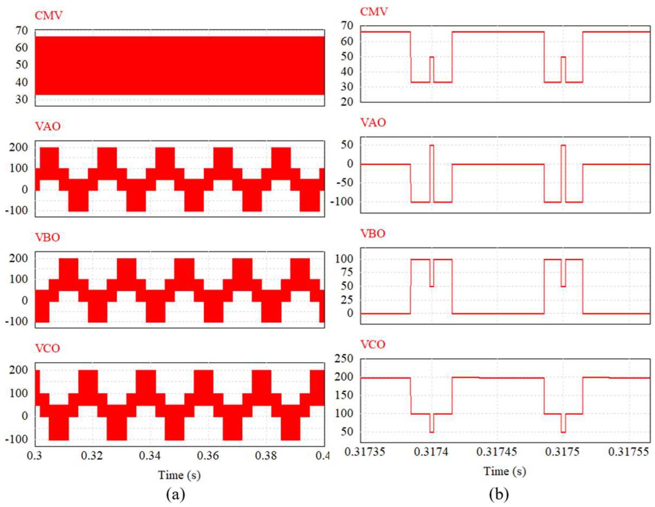
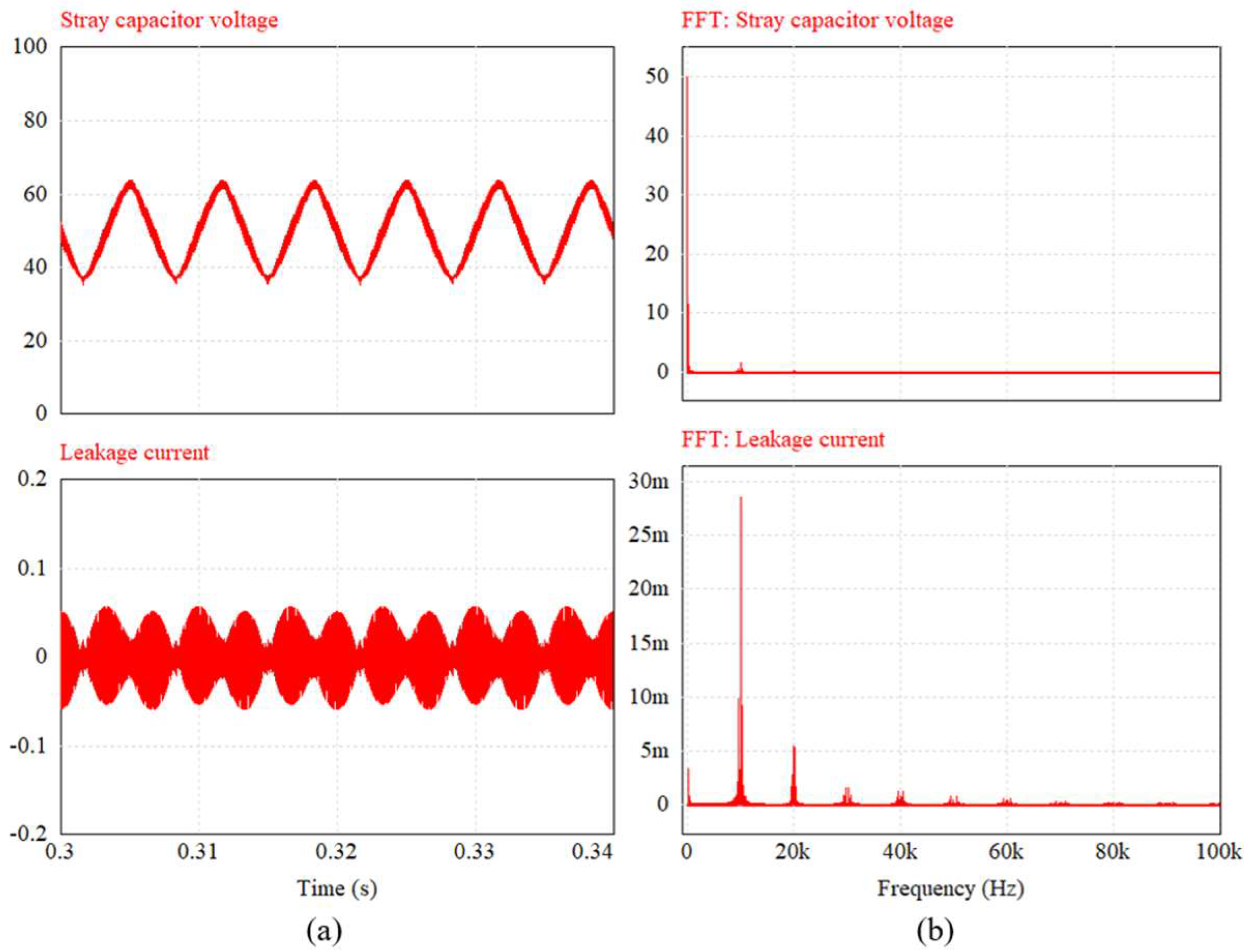
4.1. Simulation Results

To validate the operating principles and evaluate the performance of the proposed SC-qH7 inverter, simulation studies were conducted using the PSIM 9.0 software environment. The key parameters used in the simulation are given as follows. The switching frequency and the fundamental frequency were 10 kHz and 50 Hz, respectively. The two capacitors Ca and Cb were both selected as 220 µF. The DC input voltage was set to 100 V, and the stray capacitor was 300 nF. The capacitances of the additional capacitors (C0C6), as show in in Figure 2, were each set to 1 nF. An inductive load with Rl = 27 Ω and Ll = 25 mH was used.
Figure 6 presents the simulation waveforms of the proposed SC-qH7 inverter, including the input voltage, the voltages across capacitors Ca and Cb, the DC-link voltage, the voltage stress across switches Sa and Sb, and diodes Da and Db, as well as the output line-to-line voltage, output phase voltages, and their corresponding FFT analysis. As highlighted in Figure 6, the DC-link voltage VPN reached a steady-state value of 200 V, which was twice the input DC voltage. The voltage across capacitors Ca and Cb were each maintained at the input DC voltage level. The voltage stress across both switches (Sa, Sb) and both diodes (Da, Db) was observed to be equal and limited to the input voltage, confirming the reduced stress advantage of the design. As also shown in Figure 6, the inverter generated a unipolar output line-to-line voltage waveform. The output phase voltage achieved an amplitude of approximately 115 V with a modulation index M = 1. The corresponding output phase currents were sinusoidal and free from noticeable distortion. The amplitude of the output phase current was 4 A, and the THD was measured to be approximately 0.8%, demonstrating excellent power quality performance.
Figure 7 presents the simulation waveforms of the common-mode voltage and the phase voltages with respect to the negative DC terminal, i.e., the voltages between nodes A–O, B–O, and C–O, for the proposed SC-qH7 inverter. The figure also includes a zoomed-in view to clearly illustrate the CMV variation during the different operating modes. As shown in Figure 7b, during the powering modes, the CMV took discrete values of 66.6 V or 33.3 V, while during the freewheeling mode, the CMV stabilized at 50 V. These results confirm that the CMV remained bounded between 33.3 V and 66.6 V, consistent with the theoretical expectations. Consequently, the total variation in CMV was limited to 33.3 V, which corresponds to one-sixth of the DC-link voltage, demonstrating the effectiveness of the proposed SC-qH7 inverter in reducing CMV fluctuations. The waveform of the common-mode voltage across the stray capacitor CPE appeared as highlighted in Figure 8. This low CMV level contributes to a reduced leakage current in the proposed SC-qH7 inverter.
To further evaluate the inverter’s performance under varying operating conditions, the input voltage was increased to 160 V and 200 V, while the modulation index was decreased to 0.6 and 0.4, respectively. Figure 8 displays the stray capacitor voltage, corresponding leakage current, and their frequency spectra at different modulation indices. As shown in Figure 8, the higher-order harmonic components of the stray capacitor voltage remained very low across all tested conditions. The rms value of the leakage current was approximately 4 mA when M = 1 and Vdc = 100 V (Figure 8a). When the modulation index was reduced to 0.6 and the input voltage was increased to 160 V, the leakage current increased slightly to 6 mA (Figure 8b). At a further reduced modulation index of 0.4 with an input voltage of 200 V, the leakage current remained modest at 12 mA (Figure 8c). These results confirm that the proposed SC-qH7 inverter can operate across the full modulation index range while maintaining low leakage current levels, demonstrating its suitability for transformerless applications.

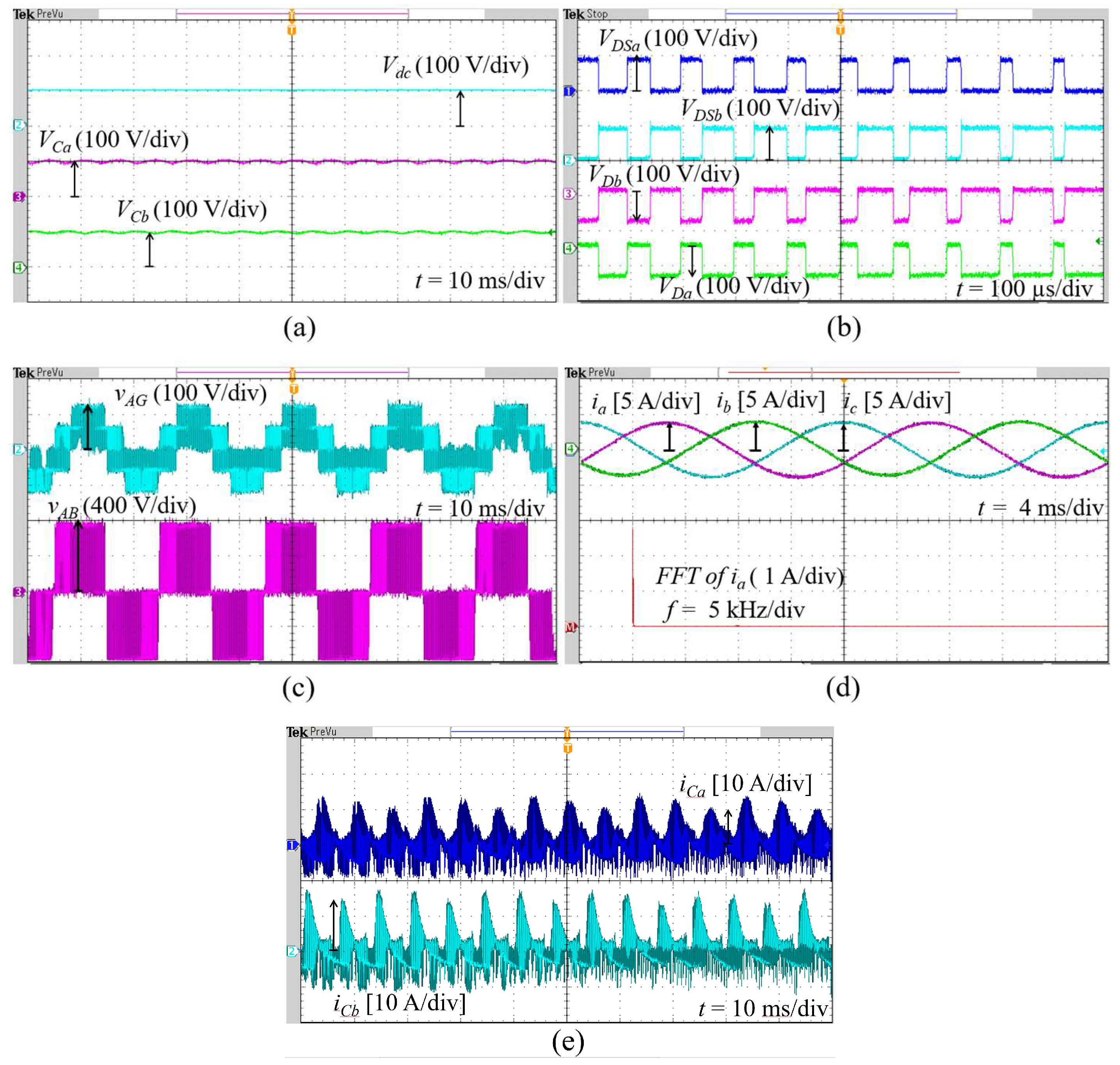
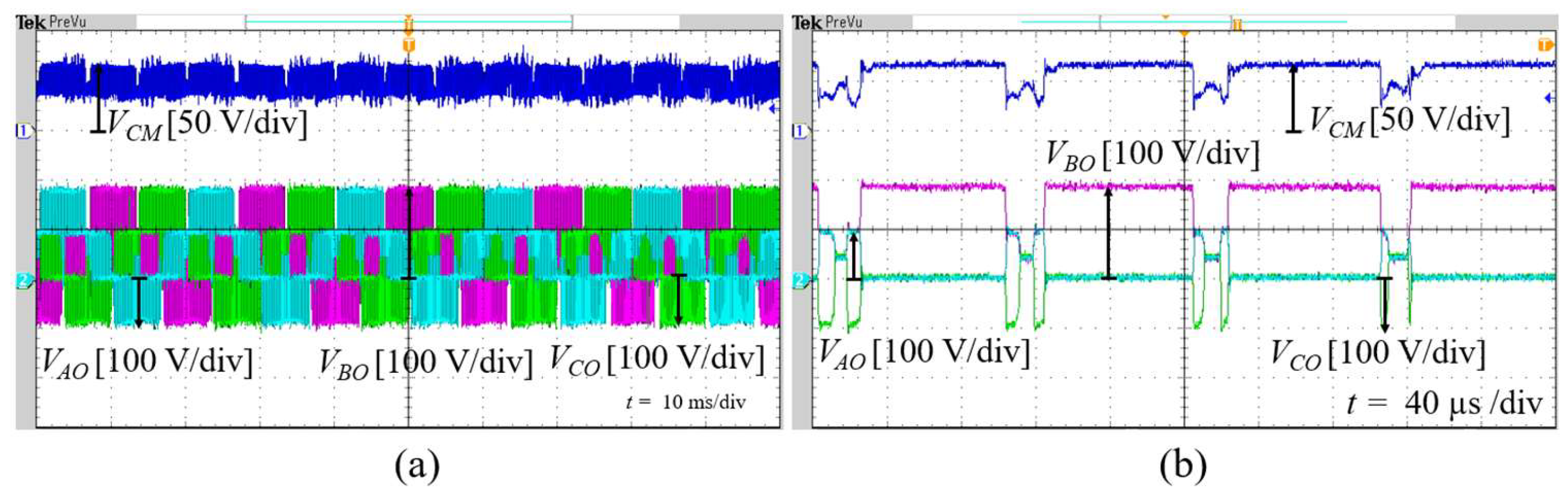
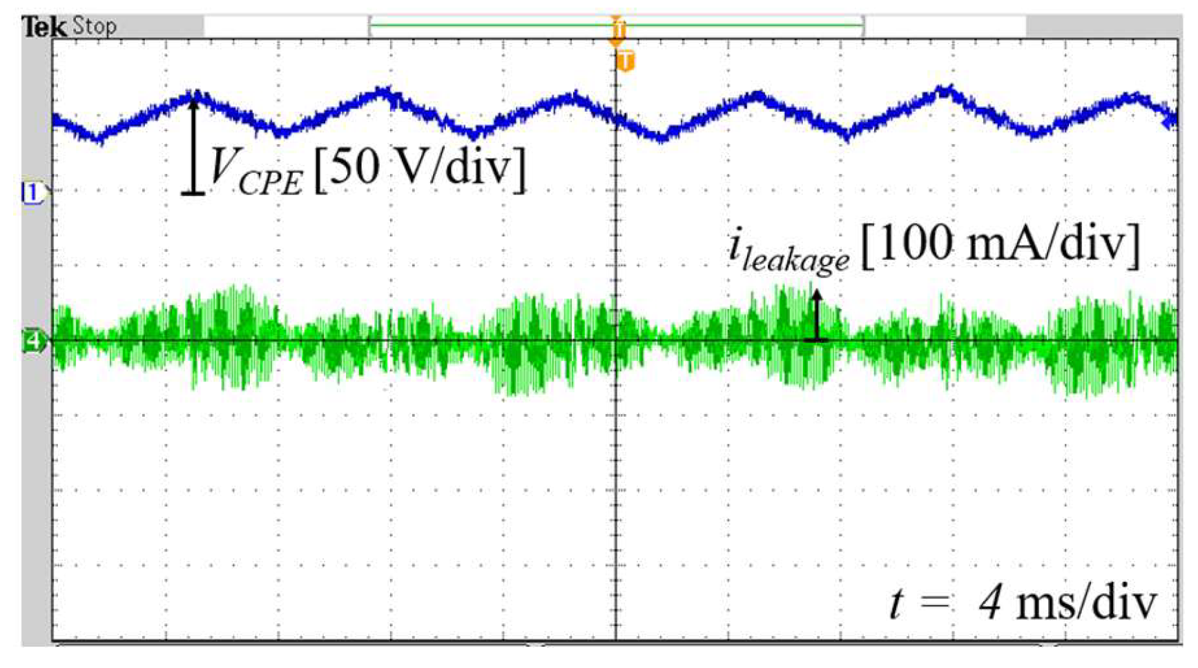
4.2. Experimental Results

In order to confirm the effectiveness of the proposed SC-qH7 inverter, a 1 kW laboratory prototype was constructed and tested. The modulation algorithms were implemented using a TMS320F28379D digital signal processor manufactured by Texas Instruments, Dallas, TX, USA, while a DE0-Nano FPGA manufactured by Intel Corporation Santa Clara, CA, USA was employed to handle logic control functions. The parameters used for the experimental setup were identical to those used in the simulation to ensure consistency in performance evaluation. For power switching, two IRFP4668PbF MOSFETs with a voltage rating of 200 V were used for switches Sa and Sb. The six H-bridge switches, along with the additional switch S0, were implemented using IPW60R045CPA MOSFETs. These eight MOSFETs were manufactured by Infineon Technologies, Neubiberg, Germany. Additionally, two STPS60SM200C Schottky diodes manufactured by STMicroelectronics, Geneva, Switzerland, with low voltage ratings were used for the freewheeling diodes Da and Db.
Figure 9 presents the experimental waveforms of the proposed SC-qH7 inverter, including the input voltage, voltages across capacitors Ca and Cb, voltage stress across switches Sa and Sb and diodes Da and Db, output line-to-line voltage vAB, output phase-A voltage, three-phase output currents, and the FFT of the output phase-A current. As shown in Figure 9a, the steady-state voltages across capacitors Ca and Cb were 98 V and 95 V, respectively. These values were slightly lower than the input voltage due to parasitic elements present in the experimental hardware. The observed low-frequency peak-to-peak ripple voltages were approximately 4 V for Ca and 6 V for Cb. Figure 9b shows that the voltage stress on switches Sa and Sb was identical at 99 V, while the voltage stresses across diodes Da and Db were 98 V and 95 V, respectively. Figure 9c confirms that the inverter generated a unipolar output line-to-line voltage waveform. As shown in Figure 9d, the output phase currents were sinusoidal and free from noticeable distortion. The measured amplitude of the output phase current was 4 A, and the THD was approximately 1.05%, validating the inverter’s high-quality output performance. The measured efficiency of the proposed SC-qH7 inverter reached approximately 90.8% when Mi = 1 at a output power of 700 W. However, the efficiency of the proposed SC-qH7 inverter was relatively low due to the use of non-optimal components in the experimental setup.
Figure 10 shows the experimental waveforms of the common-mode voltage and the voltages between nodes A-O, B-O, and C-O, along with their zoomed-in views. As shown in Figure 10a, the CMV during the powering modes took discrete values of approximately 65 V or 32 V, while it stabilized at 50 V during the freewheeling mode. This confirms that the CMV remained constrained within the expected range of 32 V to 65 V.
Figure 11 illustrates the experimental waveform of the CMV across the stray capacitor CPE, along with the corresponding leakage current. The experimental results are in good agreement with the simulation results, validating the accuracy of the proposed inverter model. It can be observed that the SC-qH7 inverter effectively limited the CMV variation, particularly during transitions into and out of mode 7. This suppression of the CMV contributed to a significantly reduced leakage current. As shown in Figure 11, the rms value of the leakage current was approximately 13.5 mA. Therefore, the proposed SC-qH7 inverter effectively limited the leakage current to a level well below 300 mA, as specified in the standard VDE-0126-1-1 [22].

5. Conclusions

In this paper, a novel three-phase two-level DC–AC inverter with low common-mode voltage, CMV, referred to as the SC-qH7 inverter, was proposed, analyzed, simulated, and experimentally validated. By integrating a voltage multiplier network into the conventional H7 inverter topology, the proposed structure achieves a DC-link voltage that is twice the input DC voltage. As a result, the SC-qH7 inverter is capable of operating in both buck and boost modes. The inverter generates a unipolar output line-to-line voltage, which reduces the voltage stress across the output filter inductor. This leads to a more compact filter design and lower power losses. Compared to conventional topologies, the SC-qH7 inverter exhibits a significantly reduced CMV, with its magnitude limited to only 16.6% of the DC-link voltage. Furthermore, the voltage stress across the additional switches in the voltage multiplier network is limited to half of the DC-link voltage, enhancing device reliability. The voltage across the stray capacitor remains low, which effectively suppresses the resulting leakage current. Simulation and experimental results confirm that the leakage current remains below 13.5 mA. Additionally, the output current THD is measured at only 1.05%, demonstrating excellent power quality. These features make the proposed SC-qH7 inverter a promising and efficient solution for three-phase transformerless photovoltaic (PV) systems. Because two capacitors in the switched-capacitor network suffer impulse charging current, the selection of the capacitors needs to meet the requirements of reliability and size of the power converter. The reliability and lifetime of the capacitors are calculated based on the switching frequency and spectral content of the impulse current through the capacitor. The size and type of the capacitor are calculated based on the level of harmonics and the lifetime of the capacitor.

Author Contributions

Conceptualization, T.-T.T. and S.-J.A.; methodology, T.-T.N.N.; software, T.-T.N.N. and M.-D.N.; validation, T.-T.T., M.-D.N. and S.-J.A.; formal analysis, T.-T.T. and S.-J.A.; investigation, S.-J.A.; resources, T.-T.T.; data curation, M.-D.N.; writing—original draft preparation, T.-T.N.N.; writing—review and editing, S.-J.A. and T.-T.T.; visualization, T.-T.T.; supervision, M.-D.N.; project administration, S.-J.A. and M.-D.N.; funding acquisition, S.-J.A. All authors have read and agreed to the published version of the manuscript.

Funding

This work was supported in part by the National Research Foundation of Korea (NRF) through the Korean Government (MSIT) under grant RS-2024-00454464.

Data Availability Statement

The original contributions presented in the study are included in the article.

Acknowledgments

Thanks to TNUT’s support in completing the article.

Conflicts of Interest

The authors declare no conflicts of interest.

References

  1. Lopez, O.; Freijedo, F.D.; Yepes, A.G.; Comesaña, P.F.; Malvar, J.; Teodorescu, R.; Gandoy, J.D. Eliminating ground current in a transformerless photovoltaic application. IEEE Trans. Energy Convers. 2010, 25, 140–147. [Google Scholar] [CrossRef]
  2. Yang, B.; Li, W.; Gu, Y.; Cui, W.; He, X. Improved transformerless inverter with common-mode leakage current elimination for a photovoltaic grid-connected power system. IEEE Trans. Power Electron. 2012, 27, 752–762. [Google Scholar] [CrossRef]
  3. Adabi, J.; Boora, A.A.; Zare, F.; Nami, A.; Ghosh, A.; Blaabjerg, F. Common-mode voltage reduction in a motor drive system with a power factor correction. IET Power Electron. 2012, 5, 366–375. [Google Scholar] [CrossRef]
  4. Murai, Y.; Kubota, T.; Kawase, Y. Leakage current reduction for a high-frequency carrier inverter feeding an induction motor. IEEE Trans. Ind. Appl. 1992, 28, 858–863. [Google Scholar] [CrossRef]
  5. Tran, T.T.; Nguyen, M.K.; Duong, T.D.; Choi, J.H.; Lim, Y.C.; Zare, F. A Switched-Capacitor-Voltage-Doubler Based Boost Inverter for Common-Mode Voltage Reduction. IEEE Access 2019, 7, 98618–98629. [Google Scholar] [CrossRef]
  6. Wang, L.; Shi, Y.; Shi, Y.; Xie, R.; Li, H. Ground leakage current analysis and suppression in a 60-kW 5-level T-type transformerless SiC PV inverter. IEEE Trans. Power Electron. 2018, 33, 1271–1283. [Google Scholar] [CrossRef]
  7. IEC 62109-2:2011; Safety for Power Converters for Use in Photovoltaic Power Systems—Part 2: Particular Requirements for Inverters. International Electrotechnical Commission: Geneva, Switzerland, 2011.
  8. Un, E.; Hava, A.M. Performance characteristics of the reduced common mode voltage near state PWM method. In Proceedings of the European Conference on Power Electronics and Applications, Aalborg, Denmark, 2–5 September 2007; pp. 1–10. [Google Scholar]
  9. Un, E.; Hava, A.M. A near-state PWM method with reduced switching losses and reduced common-mode voltage for three-phase voltage source inverters. IEEE Trans. Ind. Appl. 2009, 45, 782–793. [Google Scholar] [CrossRef]
  10. Janabi, A.; Wang, B. Hybrid SVPWM scheme to minimize the common-mode voltage frequency and amplitude in voltage source inverter drives. IEEE Trans. Power Electron. 2019, 34, 1595–1610. [Google Scholar] [CrossRef]
  11. Medekhel, L.; Hettiri, M.; Labiod, C.; Srairi, K.; Benbouzid, M. Enhancing the Performance and Efficiency of Two-Level Voltage Source Inverters: A Modified Model Predictive Control Approach for Common-Mode Voltage Suppression. Energies 2023, 16, 7305. [Google Scholar] [CrossRef]
  12. Zheng, J.; Peng, C.; Zhao, K.; Lyu, M. A Low Common-Mode SVPWM for Two-Level Three-Phase Voltage Source Inverters. Energies 2023, 16, 7294. [Google Scholar] [CrossRef]
  13. Dadu, A.M.; Mekhilef, S.; Soon, T.K.; Seyedmahmoudian, M.; Horan, B. Near State Vector Selection-Based Model Predictive Control with Common Mode Voltage Mitigation for a Three-Phase Four-Leg Inverter. Energies 2017, 10, 2129. [Google Scholar] [CrossRef]
  14. Xiaoqiang, G.; Ran, H.; Jiamin, J.; Zhigang, L.; Xiaofeng, S.; Guerrero, J.M. Leakage current elimination of four-leg inverter for transformerless three-phase PV systems. IEEE Trans. Power Electron. 2016, 31, 1841–1846. [Google Scholar]
  15. Yang, D.; Yang, K.; Gao, F. Topology Optimization Analysis of Leakage Current Suppression in Three-Level Four-Leg Photovoltaic Grid-Connected Inverter. IEEE Access 2023, 11, 50145–50156. [Google Scholar] [CrossRef]
  16. Freddy, T.K.S.; Rahim, N.A.; Hew, W.-P.; Che, H.S. Modulation Techniques to Reduce Leakage Current in Three-Phase Transformerless H7 Photovoltaic Inverter. IEEE Trans. Ind. Electron. 2015, 62, 322–331. [Google Scholar] [CrossRef]
  17. Concari, L.; Barater, D.; Buticchi, G.; Concari, C.; Liserre, M. H8 Inverter for common-mode voltage reduction in electric drives. IEEE Trans. Ind. Appl. 2016, 52, 4010–4019. [Google Scholar] [CrossRef]
  18. Rahimi, R.; Farhangi, S.; Farhangi, B.; Moradi, G.R.; Afshari, E.; Blaabjerg, F. H8 inverter to reduce leakage current in transformerless three-phase grid-connected photovoltaic systems. IEEE J. Emerg. Sel. Top. Power Electron. 2018, 6, 910–918. [Google Scholar] [CrossRef]
  19. Gupta, A.K.; Agrawal, H.; Agarwal, V. A Novel three-phase transformerless H-8 topology with reduced leakage current for grid-tied solar PV applications. IEEE Trans. Ind. Appl. 2019, 55, 1765–1774. [Google Scholar] [CrossRef]
  20. Ye, Y.; Cheng, K.W.E. A Family of Single-Stage Switched-Capacitor–Inductor PWM Converters. IEEE Trans. Power Electron. 2013, 28, 5196–5205. [Google Scholar] [CrossRef]
  21. Rosas-Caro, J.C.; Mayo-Maldonado, J.C.; Valdez-Resendiz, J.E.; Alejo-Reyes, A.; Beltran-Carbajal, F.; López-Santos, O. An Overview of Non-Isolated Hybrid Switched-Capacitor Step-Up DC–DC Converters. Appl. Sci. 2022, 12, 8554. [Google Scholar] [CrossRef]
  22. DIN VDE V 0126-1-1 VDE V 0126-1-1:2013-08; Automatic Disconnection Device between a Generator and the Public Low-Voltage Grid. VDE Publishing House: Berlin, Germany, 2013.
Figure 1. Topology of H7 inverter.
Energies 18 03218 g001
Figure 2. Topology of proposed SC-qH7 inverter.
Energies 18 03218 g002
Figure 3. Equivalent circuits of the proposed SC-qH7 inverter. (a) mode 1; (b) mode 2; (c) mode 3; (d) mode 4; (e) mode 5; (f) mode 6; (g) mode 7.
Energies 18 03218 g003
Figure 4. The frequency-domain equivalent of the proposed SC-qH7 inverter when entering mode 7.
Energies 18 03218 g004
Figure 5. DPWM strategy for the SC-qH7 inverter. (a) Space vector and A-type sectors in output of three-phase inverter; (b) switching pattern of the proposed SC-qH7 inverter in sector A1; (c) comparison of the CMV between the conventional H7 inverter and the proposed SC-qH7 inverter under the DPWM strategy.
Energies 18 03218 g005
Figure 6. Waveforms of proposed SC-qH7 inverter. From top to bottom: (a) input voltage, capacitor Ca voltage, capacitor Cb voltage, and DC-link voltage; (b) voltage across switch Sa, voltage across switch Sb, voltage across diode Da, and voltage across diode Db; (c) line-to-line voltage vAB, phase-A voltage, and 3-phase output currents (Phase A in red, Phase B in green and Phase C in blue); (d) FFT of line-to-line voltage vAB, FFT of phase-A voltage vAG, and FFT of 3-phase output currents.
Energies 18 03218 g006
Figure 7. Simulation results of common-mode voltage and the voltages between nodes A-O, B-O, and C-O of the proposed SC-qH7 inverter. (a,b) From top to bottom: CMV, vAO, vBO, and vCO.
Energies 18 03218 g007
Figure 8. Simulation results of stray capacitor voltage and leakage current for the proposed SC-qH7 inverter at different modulation indices. From top to bottom: (a,c,e) stray capacitor voltage and leakage current; (b,d,f) FFT of stray capacitor voltage and FFT of leakage current. (a,b) M = 1 and Vdc = 100 V; (c,d) M = 0.6 and Vdc = 100 V; (e,f) M = 0.4 and Vdc = 100 V.
Energies 18 03218 g008aEnergies 18 03218 g008b
Figure 9. Experimental waveforms of the proposed SC-qH7 inverter. From top to bottom: (a) input voltage, voltage across capacitor Ca, and voltage across capacitor Cb; (b) voltage stress across switches Sa and Sb and diodes Db and Da; (c) phase-A voltage and line-to-line voltage vAB; (d) three-phase output currents and FFT spectrum of output phase-A current; (e) current of capacitors Ca and Cb.
Energies 18 03218 g009
Figure 10. Experimental measurements of common-mode voltage and the voltages between nodes A-O, B-O, and C-O of the proposed SC-qH7 inverter. (a,b) From top to bottom: common-mode voltage and the voltages between nodes A-O, B-O, and C-O.
Energies 18 03218 g010
Figure 11. Experimental measurements of stray capacitor voltage (top) and leakage current (bottom) for the proposed SC-qH7 inverter.
Energies 18 03218 g011
Table 1. CMV value of conventional H7 inverter under different switching states.
Switching StateBridge States
(S1S3S5)
State of S7VCMV
State 11001Vdc/3
State 211012Vdc/3
State 30101Vdc/3
State 401112Vdc/3
State 50011Vdc/3
State 610112Vdc/3
State 71110Vdc
Table 2. CMV value and switching modes of proposed SC-qH7 inverter.
Switching ModeSwitchesDiodesOutput Leg VoltageVCM
S1S3S5SaSbS0DaDbVANVBNVCN
Mode 1OnOffOffOnOffOnOffOnVPN00VPN/3
Mode 2OnOnOffOffOnOnOnOffVPNVPN0VPN/6
Mode 3OffOnOffOnOffOnOffOn0VPN0VPN/3
Mode 4OffOnOnOffOnOnOnOff0VPNVPNVPN/6
Mode 5OffOffOnOnOffOnOffOn00VPNVPN/3
Mode 6OnOffOnOffOnOnOnOffVPN0VPNVPN/6
Mode 7OnOnOnOffOnOffOffOn000VPN/4
VPN is the DC-link voltage across the H-bridge circuit.
Table 3. Switching pattern of the DPWM strategy for the SC-qH7 inverter.
SectorSwitching Sequence
A1 V 7 ( 111 ) - V 2 ( 110 ) - V 1 ( 100 ) - V 1 ( 100 ) - V 2 ( 110 ) - V 7 (111)
A2 V 7 ( 111 ) - V 2 ( 110 ) - V 3 ( 010 ) - V 3 ( 010 ) - V 2 ( 110 ) - V 7 (111)
A3 V 7 ( 111 ) - V 4 ( 011 ) - V 3 ( 010 ) - V 3 ( 010 ) - V 4 ( 011 ) - V 7 (111)
A4 V 7 ( 111 ) - V 4 ( 011 ) - V 5 ( 001 ) - V 5 ( 001 ) - V 4 ( 011 ) - V 7 (111)
A5 V 7 ( 111 ) - V 6 ( 101 ) - V 5 ( 001 ) - V 5 ( 001 ) - V 6 ( 101 ) - V 7 (111)
A6 V 7 ( 111 ) - V 6 ( 101 ) - V 1 ( 100 ) - V 1 ( 100 ) - V 6 ( 101 ) - V 7 (111)
Disclaimer/Publisher’s Note: The statements, opinions and data contained in all publications are solely those of the individual author(s) and contributor(s) and not of MDPI and/or the editor(s). MDPI and/or the editor(s) disclaim responsibility for any injury to people or property resulting from any ideas, methods, instructions or products referred to in the content.

