Abstract
This paper describes active battery balancing based on a bidirectional buck converter, a flyback converter, and battery cells by using the proposed chain-loop comparison strategy. The role of the bidirectional buck converter is to charge/discharge the battery pack. During the charging period, the converter is in buck mode, and its output is controlled by constant current/voltage; during the discharging period, the converter is in boost mode, and its output is controlled by constant voltage. The role of the flyback converter is voltage equalization of the battery pack, and its output is controlled by constant current. A chain-loop comparison strategy is used to control battery voltage equalization. In this work, three equalization modes, namely, charging balance, discharging balance, and static balance, were considered. The voltage difference between the maximum and minimum is 0.007 V after a balancing time of 19.75 min, 0.005 V after a balancing time of 24 min, and 0.007 V after a balancing time of 20 min for charging balance, discharging balance, and static balance, respectively.
1. Introduction
A single lithium battery cell is not sufficient to meet the demand of modern appliances due to the increase in human demand for electricity and the different power specifications required by products. To solve this problem, cells are connected in series to increase the voltage and in parallel to increase the capacity to form a pack to meet the system specifications. It is generally recognized that each battery cell has different features [1,2,3,4], such as capacity, impedance, self-discharge rate, and aging, thereby making voltage imbalance between the battery cells occur when the batteries are in operation. If a battery pack continues to be used in an imbalanced condition, the battery cells will be overcharged/discharged, the battery life will be shortened, and in severe cases, the battery pack will explode [3,4]. Therefore, it is necessary to use a battery balancing circuit in order to allow the battery pack to operate safely for a long period of time. Battery balancing circuits are divided into two groups [5,6,7,8,9,10,11,12,13,14,15], passive balancing and active balancing, as shown in Figure 1.
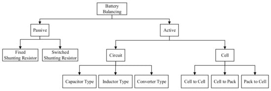
Figure 1.
Classification of battery balancing.
In the case of passive balancing, as shown in Figure 1, the method of Reference [16] is to put a resistor on each battery cell, through which the higher-voltage battery cell is depleted until it matches and balances the voltage of other battery cells. The approach of Reference [17] improves on Reference [16] by adding a switch to prevent the resistor from continuously consuming, which requires the battery cell voltage to be detected, and the corresponding switch is turned on if the battery cell voltage is higher. Energy is consumed in the resistors in both methods mentioned above, and hence heat is generated in the resistors. Therefore, these methods waste energy, but they have the advantages of simple structure and low cost.
Active balancing, as shown in Figure 1, is mainly for energy recycling and is more efficient than passive balancing, but the structure of this method is complicated, and the cost is higher. Active balancing can be analyzed from the circuit and the battery perspectives.
As shown in Figure 1, circuits can be divided into three types: capacitor, inductor, and converter. Capacitors [18,19,20,21,22,23] are used as energy storage elements between the battery cells by switching the control to form a loop to achieve energy transfer. An advantage of this method is that the volume of a capacitor is smaller than that of a magnetic component. However, the balance current is determined by the difference in voltage between the battery cells, so the cells are inevitably balanced by slow speed and inrush current. The inductor type [24,25,26,27,28] involves the inductive energy transfer from the battery cells or the battery pack to the battery cells or the battery pack, and this method is characterized by its ability to provide a larger balance current and significantly shorten the balance time. Therefore, compared to the capacitive method, the balancing time is relatively short, but the size of the magnetic component is larger. In addition, when using a multi-winding transformer, the complexity of the transformer design increases, and the need to ensure that each winding has the same characteristics makes the entire system more complex and bulky. Common circuit topologies are usually employed, such as the Cuk converter [29], flyback converter [30,31,32], buck–boost converter [33], and forward converter [34]. This method has more freedom to allow the battery to equalize the voltage, so the balancing effect is better than that of other methods, but the structure is more complicated compared to passive balancing.
As shown in Figure 1, batteries can be divided into three modes, i.e., cell-to-cell (C2C), cell-to-pack (C2P), and pack-to-cell (P2C), and these modes should be combined with active balancing to achieve battery balancing along with a capacitor, inductor, or converter.
The C2C mode uses the higher-voltage cell to transfer energy to the lower-voltage cell through the capacitor, inductor, or converter to achieve battery voltage equalization. This structure requires the addition of multiple sets of switches to connect the battery cells, thereby increasing the losses caused by the switches. However, the control is simpler, and the circuits are often modularized, which is known as individual cell equalization (ICE). Reference [29] reports the use of a battery equalization module for voltage balancing. This module combines the neighboring cells plus the Cuk converter to achieve C2C battery voltage equalization. The balancing speed of the neighboring cells in this structure is faster than those of other structures, and this is because of the converter across the battery cell. However, if voltage balancing is required for distant cells, the balancing speed will be slower because the energy needs to be transferred through other cells. Consequently, in order to improve the method of [29], References [35,36] divided the battery voltage equalization module into cell modules and a module composed of cell modules for battery balancing. In their method, the balancing speed is faster, but the circuit is more complicated, and the number of required components is significantly higher. Reference [37] combines the buck–boost converter and the switched-capacitor converter. In addition, the inductor is changed to a coupled inductor. If the imbalanced cells are far away from each other, the energy will be transferred through the coupled inductor and the switched capacitor, so the balancing speed is faster. Reference [38] combines a switched-capacitor converter and an external LC resonant circuit. The switched-capacitor converter is used for battery balancing when the maximum voltage difference between the cells is large, while the LC resonant circuit is used for battery balancing when the maximum voltage difference between the cells is small. By doing so, the disadvantage of capacitive balancing is solved; however, if the voltage difference is too small, the balancing speed will be slowed down.
The cell-to-pack mode utilizes the higher-voltage cell to transfer energy to the battery pack through a capacitor, inductor, or converter to achieve battery voltage equalization, while in the case of the P2C mode, this is achieved by utilizing a battery pack to transfer energy to the lower-voltage cell through a capacitor, inductor, or converter. Both approaches have more regulation methods than the cell-to-cell mode, allowing multiple cells to be equalized at the same time. However, because of the connection to the battery pack, the parts are subjected to higher voltage stresses. Reference [39] proposes the division of the batteries into modules for balancing, and each module corresponds to a winding for voltage equalization, so the number of transformers can be reduced. In the P2C mode, an area with an even or odd number of cells can be utilized to perform voltage equalization, so if the same module has two cells with lower voltage, the voltage balancing takes more time. In order to connect each cell, the required number of switches is much higher, and a bidirectional switch must be used to increase the conduction loss and switching loss.
Reference [40] uses a bidirectional non-isolated DC–DC converter for the battery voltage equalization of the P2C and C2P modes, and the circuit behavior can be classified into the buck mode or the boost mode. Due to the use of a non-isolated converter, the main circuit’s mode of judgment is based on the last battery cell, so it needs to withstand continuous charging and discharging, which affect the battery life. Reference [41] reports charge balancing where the main structure is a buck-derived converter, which is combined with a charger and a voltage equalizer. The inductor of the buck converter of the charger is replaced with a multi-winding transformer, and the transformer output is connected to its corresponding battery cell for battery balancing, so there is no need for additional active switching and control. However, accurate control over the balancing current cannot be achieved. Reference [42] adopts two flyback converters for battery voltage equalization. The corresponding operating principle is to first magnetize one of the coupled inductors of the high-voltage battery cell, and when this coupled inductor is demagnetized, the rechargeable battery pack magnetizes the other coupled inductor at the same time, and when the other coupled inductor is demagnetized, the low-voltage battery cell is recharged. Although this topology is simple and easy to control, which helps to reduce the cost of the battery balancing system, it has the disadvantage of additional losses due to the need for additional switches and diodes. Reference [43] outlines a combination of a power supply and voltage equalizer so that the number of power supplies can be reduced. Although this circuit is mainly based on a bidirectional flyback converter, this structure only has discharge balancing. Its modes are divided into the cell-to-load (C2L) mode and the battery C2C mode, and the efficiency of the converter needs to be especially considered because the voltage equalizer of this structure is related to the main power stage. In addition, in the battery C2C mode, the converter passes through two converters, so there is a larger loss. Reference [44] details a simple fault-tolerant control (FTC) technique based on online vector calculation and a constraint mechanism to balance DC voltage for a single-phase cascaded H-bridge multilevel converter (CHBMC).
2. System Configuration
A battery voltage equalizer with a bidirectional buck converter and a flyback converter for charging balance, discharging balance, and static balance is presented herein. The system configuration is shown in Figure 2. A Cyclone III EP3CE144C8N FPGA is used to control the proposed circuit system. This bidirectional buck converter is a battery charger, and its control mode is set to a constant current/constant voltage (CC/CV) to charge the battery during charging. In addition, this circuit has a bidirectional function, so it can discharge the battery and supply power to the load, and its control mode is set to a constant voltage (CV). The primary side of the flyback converter is connected to the low-voltage side of the bidirectional buck converter and the battery pack, and the secondary side of the flyback converter is connected to each corresponding battery cell. A voltage-chasing method, called chain-loop comparison, is proposed for battery voltage equalization. This method involves detection of the voltage of each battery cell and determining whether the corresponding flyback converter is activated or not by comparing each battery cell based on the chain loop. In addition, OPA1 is used as a difference amplifier with filters to sense the voltage across RsiL to obtain the current IiL flowing through the bidirectional buck converter, whereas OPA2 to OPA5 are used as difference amplifiers without any filters to sense the battery voltages Vb1_s, Vb2_s, Vb3_s, and Vb4_s. The voltages Vbuck and Vboost of the bidirectional buck converter are sensed by the voltage divider, and the currents Iob1, Iob2, Iob3, and Iob4 of the secondary-side DC currents of the flyback converters are sensed by the hall current sensors. These sensed voltages mentioned above are sent to the FPGA to generate gate driving signals for the switches.
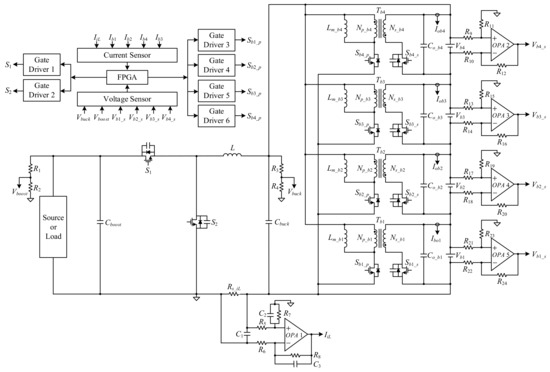
Figure 2.
Proposed system configuration.
3. Operating Principle of the Battery Voltage Equalizer
In order to facilitate the analysis, Figure 2 was converted into a block diagram as shown in Figure 3. Prior to explaining the operating principle, the associated symbols in Figure 3 are defined first. Since four series of three parallel lithium batteries are used in this design, the voltage balance is composed of four flyback converters and four series of lithium batteries. In the equalizer presented in this paper, the total current flowing into the flyback converter is Iin_bT; the primary-side currents are Iin_b1, Iin_b2, Iin_b3, and Iin_b4; and the secondary-side currents are Io_b1, Io_b2, Io_b3, and Io_b4 and are maintained at 2 A during the operation of the flyback converters. The battery cells flow through the currents Ib1_T, Ib2_T, Ib3_T, and Ib4_T, and the current through the battery pack is Ipack. Table 1 shows the possible cases of the operating principles for four flyback converters based on the voltage-chasing method, where 1 means the flyback converter is in operation, and 0 means the flyback converter is not in operation.
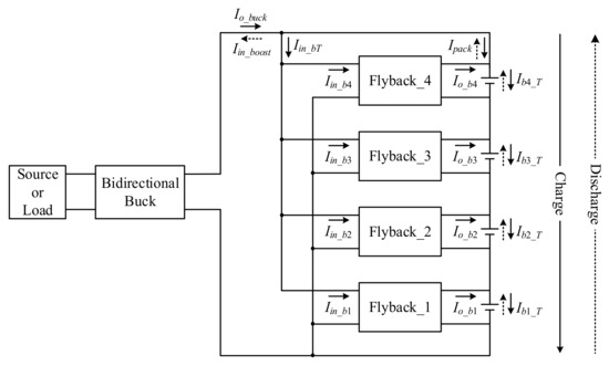
Figure 3.
Simplified block diagram of the proposed system for battery charging and discharging with additional symbols included.

Table 1.
Possible cases of the operating principles for four flyback converters.
3.1. Charging Balance
Figure 4 shows the schematic diagram of the charging balance. In this state, the bidirectional buck converter provides a stable current source Io_buck to supply energy to the flyback converter and the battery pack, so the final current Ipack through the battery pack can be obtained as shown in (1). The total input current Iin_bT of the flyback converters is shown in (2), and the current flowing through each battery is shown in (3) to (6):
Figure 4.
Schematic diagram of charging balance.
If the battery voltage is Vb4 > Vb3 > Vb2 > Vb1, using the proposed chain-loop comparison method, we can determine that Vb4 > Vb3, implying that Flyback_3 is on and Flyback_4 is off; Vb3 > Vb2, implying that Flyback_2 is on and Flyback_3 is off; Vb2 > Vb1, implying that Flyback_1 is on and Flyback_2 is off; and Vb4 > Vb1, implying that flyback_1 is on and Flyback_4 is off.
By summarizing the above, it can be seen that Flyback_1, Flyback_2, and Flyback_3 are on, but Flyback_4 is off, as shown in Figure 5, which corresponds to case 15 in Table 1. Equations (2) and (6) can be rewritten as (7) and (8), respectively, while Equations (1) and (3)–(5) remain unchanged. Since three flyback converters are on, the stabilized current source Io_buck provides part of the current to the flyback converter Iin_bT, which reduces battery pack current Ipack, thereby slowing the charge speed of the battery with the highest voltage Vb4. In addition, the batteries with the voltages Vb3, Vb2, and Vb1 are charged by the battery peak current Ipack plus the stable current of 2 A provided by the individual flyback converters, thus increasing the charging speed so that the battery voltage of Vb3, Vb2, and Vb1 can catch up with that of Vb4 to achieve the purpose of charging balance:
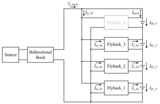
Figure 5.
Case 15 of charging balance.
When the battery is balanced in case 1, as shown in Figure 6, Flyback_1, Flyback_2, Flyback_3, and Flyback_4 are turned off, and the associated equation is (9):
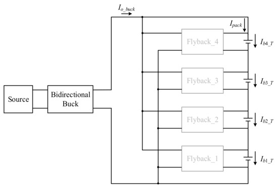
Figure 6.
Case 1 of charging balance.
3.2. Discharging Balance
Figure 7 shows the schematic diagram of the discharging balance. In this state, the battery pack has to provide energy to the bidirectional buck converter and provide energy to the flyback converter so that we can determine the final current Ipack through the battery pack as shown in (10). The total input current of the flyback converters, Iin_bT, is shown in (2), and the current flowing through each battery is shown in (11) to (14):
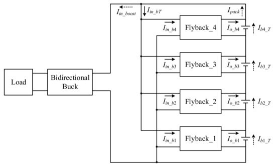
Figure 7.
Schematic diagram of discharging balance.
If the battery voltage is Vb4 < Vb3 < Vb2 < Vb1, using the proposed chain-loop comparison method, we can determine that Vb4 < Vb3, implying that Flyback_4 is on and Flyback_3 is off; Vb3 < Vb2, implying that Flyback_3 is on and Flyback_2 is off; Vb2 < Vb1, implying that Flyback_2 is on and Flyback_1 is off; and Vb4 < Vb1, implying that Flyback_4 is on and Flyback_1 is off. By summarizing the above, it can be seen that Flyback_2, Flyback_3, and Flyback_4 are off, but Flyback_1 is on as shown in Figure 8, which corresponds to case 8 in Table 1. Here, Equations (2) and (11) can be rewritten as (15) and (16), respectively, while Equations (10) and (12)–(14) remain unchanged. Since three flyback converters are on, the battery pack provides part of the current to the flyback converter Iin_bT and also provides part of the current to the bidirectional buck converter Iin_boost, in which the batteries with lower voltages Vb2, Vb3, and Vb4 can be made up by the stable current of 2 A provided by the individual flyback converters. Thus, the current provided by these batteries is reduced, and the battery with the highest voltage Vb1 discharges more current so as to achieve the purpose of discharging balance:
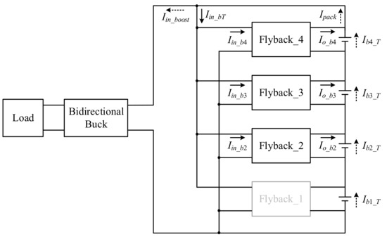
Figure 8.
Case 8 of discharging balance.
When the battery is balanced in case 1, as shown in Figure 9, Flyback_1, Flyback_2, Flyback_3, and Flyback_4 are turned off, and the associated equation is shown in (17):
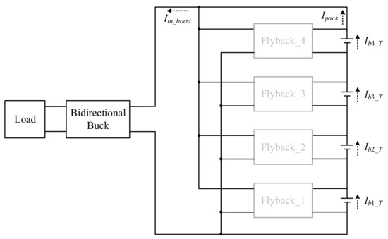
Figure 9.
Case 1 of discharging balance.
3.3. Static Balance
Figure 10 shows the schematic diagram of static balancing, which is performed when there is no load or power supply and the batteries have uneven voltages. In this state, the battery pack has to provide energy to the flyback converter, so the current Ipack through the battery pack can be obtained as shown in (18), where the total current of the flyback converters Iin_bT is shown in (2), and the current flowing through each battery is shown in (11) to (14).
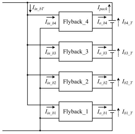
Figure 10.
Schematic diagram of static balance.
If the battery voltage is Vb3 > Vb1 > Vb4 > Vb2, using the proposed chain-loop comparison method, we can determine that Vb4 < Vb3, implying that Flyback_4 is on and Flyback_3 is off; Vb3 > Vb2, implying that Flyback_2 is on and Flyback_3 is off; Vb2 < Vb1, implying that Flyback_2 is on and Flyback_1 is off; Vb4 > Vb1, implying that Flyback_1 is on and Flyback_4 is off; Vb2 < Vb1, implying that Flyback_2 is on and Flyback_1 is off; and Vb4 > Vb1, implying that Flyback_1 is on and Flyback_4 is off. By summarizing the above, we can see that Flyback_2 and Flyback_4 are on, but Flyback_1 and Flyback_3 are off, as shown in Figure 11, which corresponds to case 6 in Table 1. Here, Equations (2), (11) and (13) can be rewritten as (19), (16), and (20), respectively, while Equations (12) and (14) remain unchanged. Since two flyback converters are on, the battery pack provides part of the current to the flyback converter Iin_bT, where the batteries with the lower-voltage cells Vb2 and Vb4 can be made up by the stable current of 2 A provided by the individual flyback converters. Therefore, the current discharged by these batteries is reduced, and the batteries with the voltages Vb1 and Vb3 discharge more current so as to achieve a static balance:
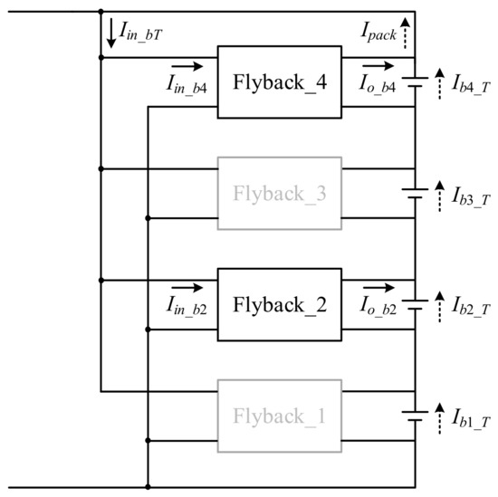
Figure 11.
Static balance of case 6.
When the battery is balanced in case 1, as shown in Figure 12, Flyback_1, Flyback_2, Flyback_3, and Flyback_4 are turned off, and the associated equation is (21):
Figure 12.
Static balance of case 1.
4. Design Considerations
Table 2.
Specifications of bidirectional buck converter in buck mode.
Table 3.
Specifications for bidirectional buck converter in boost mode.
Table 4.
Flyback converter specifications.
Table 5.
Battery cell specifications.
4.1. Circuit Parameter Design
This subsection will describe the circuit parameter design in detail, including the inductance, magnetizing inductance, and capacitance.
4.1.1. Inductance Design for Bidirectional Buck Converter
In the design of the inductor, the buck mode was chosen. The boundary output current was set to 2 A. When the output current is lower than this current, the inductor current iL becomes a negative value. The input voltage Vin_buck is 48 V, and the output voltage Vo_buck is 16.8 V, so the corresponding duty cycle Dbuck is 0.35. Therefore, the value of the inductor is 18.2 μH:
In order to ensure that the inductor current iL of 2 A or more is free from negative current over the entire operating range, an inductance of 23 μH was selected.
4.1.2. Output Capacitance Design for the Bidirectional Buck Converter
The designs of the output capacitances for the buck and boost modes are detailed in the following.
Output Capacitance Cbuck in Buck Mode
Figure 13 shows the key waveforms for calculating the capacitance in buck mode of the bidirectional buck converter. According to the Ampere-second balance, the average current flowing into the capacitor in one cycle in steady state is zero, so the values of ∆Q+ and |∆Q−| are equal and can be expressed as (23), where ∆Vo_buck is the output voltage ripple in buck mode:
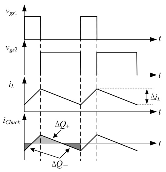
Figure 13.
Key waveforms of output capacitor in buck mode.
Since ∆iL is the peak-to-peak value of the inductor current, Equation (23) can be rewritten as (24):
Assuming that the output voltage ripple is less than 1%,
Substituting (25) into (24) and rearranging this result with associated values yields
Finally, by considering the effect of frequency on the capacitance, the actual value should be chosen to be higher than the calculated value, so a 220 µF/50 V electrolytic capacitor was selected.
Output Capacitance Cbuck in Boost Mode
Figure 14 shows the key waveforms for calculating the capacitance in boost mode of the bidirectional buck converter. The average current flowing into the capacitor in one cycle in steady state is zero, so the values of ∆Q+ and |∆Q−| are identical and can be expressed as (27), where ∆Vo_boost is the output voltage ripple in boost mode.
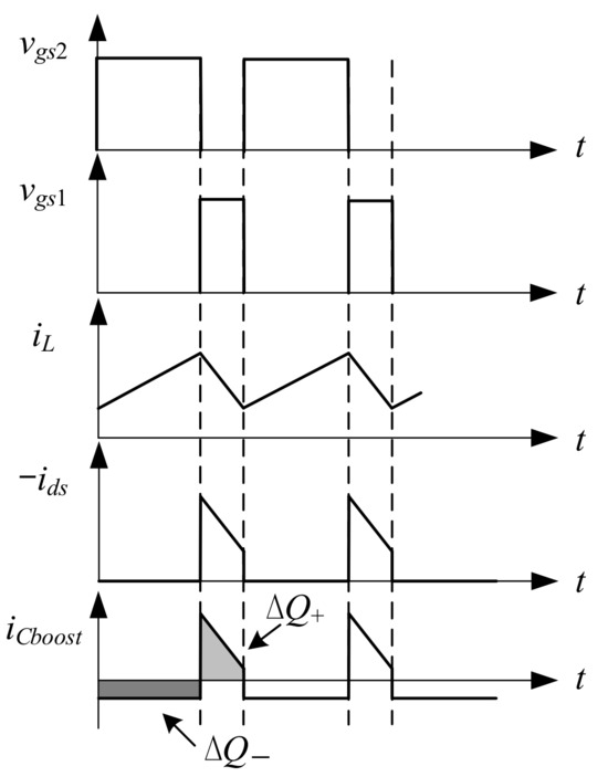
Figure 14.
Key waveforms of the output capacitor in boost mode.
Rearranging (27) yields
Assuming that the output voltage ripple is less than 1%,
Substituting (29) into (28) and rearranging this result with associated values yields
Finally, by considering the effect of frequency on the capacitance, the actual value should be chosen to be higher than the calculated value, so a 220 µF/100 V electrolytic capacitor was selected.
4.1.3. Magnetizing Inductance Design for Flyback Converter
In order to ensure that the circuit can be maintained in DCM, the sum of the magnetizing time ratio Dx1 and the demagnetization time ratio Dx2 of the magnetizing inductance Lm_b was set to 0.85, i.e.,
From the voltage conversion ratio Mb in (32), the demagnetization time ratio Dx2 can be rewritten as
Substituting (33) into (31) yields
From (31) and (34), the equations of Dx1 and Dx2 can be obtained as
By substituting (34) and (35) into (36), the output current Io_b can be obtained as
Since the converter is operated in DCM, Equation (37) can be rewritten as (38), and then the value of Dmax in (31), the output current Io_b of 2 A, the turns ratio Np_b/Ns_b of 4, and the maximal and minimal output and input voltages in Table 4 are substituted into the Equation (38) to draw the curves of relationship between Lm_b and Vo_b. This is shown in Figure 15, with the dotted line as the minimum input voltage Vin_b_min for each battery and the solid line as the maximum input voltage Vin_b_max. From this figure, the minimum magnetizing inductance can be found to be 33.37 µH, and the actual magnetizing inductance was chosen to be 29 µH to ensure that the converter can be operated in DCM.
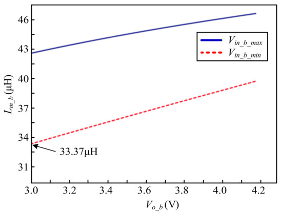
Figure 15.
Curves of the relationship between Lm_b and Vo_b at maximum and minimum input voltages.
4.1.4. Output Capacitance Design for Flyback Converter
Figure 16 shows the illustrated waveforms of the output capacitor of the flyback converter. Firstly, the related value of x should be calculated, and Equation (39) can be written by using the similar triangle, where Isd_s_peak is the peak current on the switch Sb_p, and ∆isd_s_peak is the peak-to-peak current on the switch Sb_p:
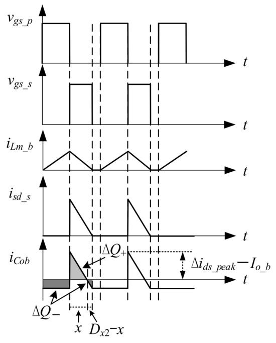
Figure 16.
Illustrated waveforms of the output capacitor.
According to the Ampere-second balance, the average current flowing into the capacitor in one cycle in steady state is zero, so the values of ∆Q+ and |∆Q−| are equal, and ∆Q+ can be expressed as (40), where ∆Vo_b is the output voltage ripple of the flyback converter.
By assuming that the output voltage ripple is less than 1%, it can be found that
By substituting (41) into (40), (42) can be obtained, and the associated values are substituted into (42) and plotted in Figure 17, from which the highest output capacitance can be found to be 659.42 µF:
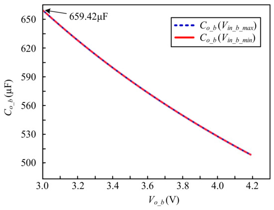
Figure 17.
Curves of relationship between Co_b and Vo_b at maximum and minimum input voltages.
Finally, by considering the effect of frequency on the capacitance, the actual value was chosen to be higher than the calculated value, so a 1500 µF/50 V electrolytic capacitor was selected.
5. Control Considerations
In control strategies for converters in different modes, a field-programmable gate array (FPGA) is used as a digital controller; the chip used is a Cyclone III EP3CE144C8N, and the required functions inside the FPGA are described by the hardware description language (HDL).
5.1. Control Strategies for Converters in Different Modes
Figure 18 shows the control strategy of the bidirectional buck converter in buck mode, which consists of two analog-to-digital converters (ADCs) to sample signals Vbuck and IiL shown in Figure 2, two PI controllers, a constant current and constant voltage multiplexer (CC/CV MUX), a pulse-width-modulated (PWM) generator, and two blanking time generators. This control strategy is mainly for CC/CV control. The voltage and current feedback signals Vbuck and IiL shown in Figure 18 are converted into digital data by the ADCs, and after this, the digital commands Ref1 and Ref2 are subtracted from the corresponding digital data to generate the error values, which are then sent to the PI controllers to create the required control force. These control forces are sent to the CC/CV to determine the control authority and finally sent to the PWM generator to yield the required gate driving signals to drive the switches.
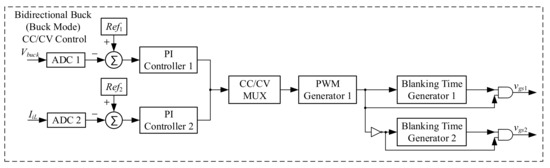
Figure 18.
Control strategy for the bidirectional buck converter in buck mode.
Figure 19 shows the control strategy of the bidirectional buck converter in boost mode, which is composed of an ADC, a PI controller, a PWM generator, and two blanking time generators. This control strategy is mainly for CV control. The feedback signal Vboost of the voltage shown in Figure 19 is converted into digital data by the ADC, and then the digital command Ref3 is subtracted from the digital data to generate the error value, which is sent to the PI controller to generate the required control force and finally sent to the PWM generator to yield the required gate driving signal to drive the switch.
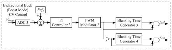
Figure 19.
Control strategy for the bidirectional buck converter in boost mode.
Figure 20 shows the control strategy of the four flyback converters, which consist of four ADCs, four PI controllers, and four PWM generators. This control strategy is mainly for CV control. The four feedback signals Io_b1, Io_b2, Io_b3, and Io_b4 in Figure 20 are converted to digital data by individual ADCs, and then the corresponding digital commands Ref1, Ref2, Ref3, and Ref4 are subtracted from these digital data to generate the error values, which are sent to individual PI controllers to generate the required control forces and then sent to the PWM generators to yield the required duty cycles. Finally, these duty cycles perform an AND logic operation with the signals Ctrlb1, Ctrlb2, Ctrlb3, and Ctrlb4 created from chain-loop comparison so as to obtain the gate driving signals to drive the switches.
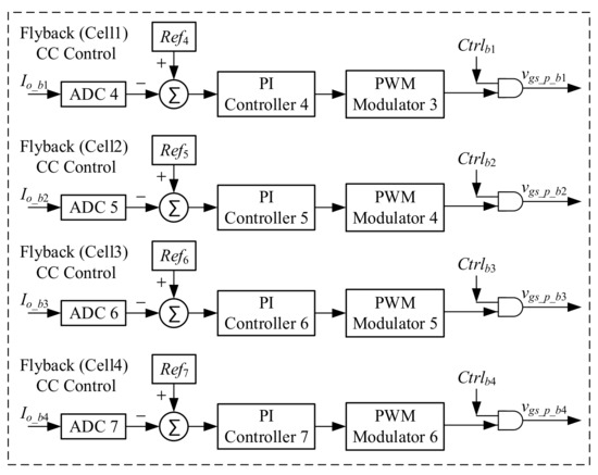
Figure 20.
Control strategy for flyback converters.
5.2. Chain-Loop Comparison Signals
Figure 20 shows the control strategy of the flyback converters, where the chain-loop comparison signals Ctrlb1, Ctrlb2, Ctrlb3, and Ctrlb4 are used to decide whether to activate the flyback converter corresponding to each battery for battery balancing. Figure 21 shows the flowchart of the chain-loop comparison strategy, and Figure 22 shows the operation diagram of the chain-loop comparison strategy. From Figure 22, it can be seen that there are two comparison values for each battery: Ctrlb1_1 and Ctrlb1_2, Ctrlb2_1 and Ctrlb2_2, Ctrlb3_1 and Ctrlb3_2, and Ctrlb4_1 and Ctrlb4_2 for the first, second, third, and fourth batteries, respectively. After chain-loop comparison, these two pieces of data are aggregated by an OR logic operation to obtain the chain-loop comparison signals of each of the four batteries, namely, Ctrlb1, Ctrlb2, Ctrlb3, and Ctrlb4.
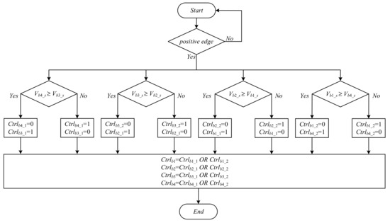
Figure 21.
Flowchart of chain-loop comparison signals.
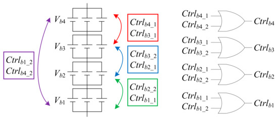
Figure 22.
Operation diagram of chain-loop comparison signals.
6. Experimental Results
In this section, some experimental waveforms and measurements are shown below.
6.1. Experimental Results for Charging Balance
Figure 23 shows the experimental results for charging balance, in which the initial values of the batteries are 3.507 V for Vb4, 3.397 V for Vb3, 3.25 V for Vb2, and 3.092 V for Vb1. It can be found that at this time the voltage difference between the maximum and minimum is 0.415 V, and after the proposed chain-loop comparison for battery balancing, the voltages of the four batteries after 19.75 min are 4.0 V for Vb4, 3.997 V for Vb3, 3.995 V for Vb2, and 3.993 V for Vb1. After battery balancing, the voltage difference is 0.007 V, and the four battery voltages converge to 3.99 V.
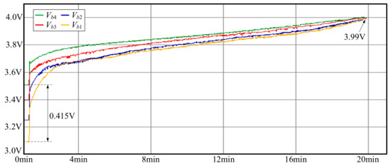
Figure 23.
Experimental results for charging balance.
6.2. Experimental Results for Discharging Balance
Figure 24 shows the experimental results for discharge balancing, in which the initial values of the batteries are 3.985 V for Vb4, 3.839 V for Vb3, 3.803 V for Vb2, and 3.566 V for Vb1. It can be found that the voltage difference between the maximum and minimum at this time is 0.419 V, and after battery balancing through the proposed chain-loop comparison, the voltages of the four batteries after 24 min are 3.338 V for Vb4, 3.336 V for Vb3, 3.334 V for Vb2, and 3.333 V for Vb1. After battery balancing, the battery voltage difference is 0.005 V, and the four battery voltages converge to 3.335 V.
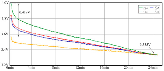
Figure 24.
Experimental results for discharging balance.
6.3. Experimental Results for Static Balance
Figure 25 shows the experimental results for static balance, in which the initial values of the batteries are 3.756 V for Vb4, 3.716 V for Vb3, 3.357 V for Vb2, and 3.249 V for Vb1. It can be found that the voltage difference between the maximum and minimum at this time is 0.507 V. After the proposed chain-loop comparison, the voltages of the four batteries after 20 min are 3.482 V for Vb4, 3.479 V for Vb3, 3.477 V for Vb2, and 3.475 V for Vb1. After battery balancing, the voltage difference between the maximum and minimum is 0.007 V, and the four battery voltages converge to 3.478 V.
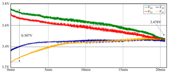
Figure 25.
Experimental results for static balance.
6.4. Experimental Waveforms of Converters
In this subsection, some measured waveforms related to the converters are shown.
Figure 26 and Figure 27 show that the closed-loop control allows the bidirectional buck converter in buck mode to be controlled at a constant current and a constant voltage, respectively. Figure 28 shows that the closed-loop control allows the bidirectional buck converter in boost mode to be controlled at a constant voltage. Figure 29 shows that the voltage across the primary-side switch Sb_p, called vds_p, and the voltage across the secondary-side switch Sb_s, called vds_s, allow the flyback converter to be operated in DCM. This is because when the magnetizing inductance Lm_b is fully demagnetized, it resonates with the equivalent output capacitance of the switch Sb_p, which generates oscillations and maps them to the secondary side. Figure 30 shows that the closed-loop control allows the flyback converter to be controlled at a constant current.
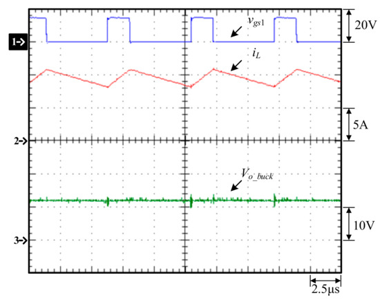
Figure 26.
Measured waveforms of the bidirectional buck converter in buck mode with an output voltage of 12 V and a constant current of 10 A: (1) vgs1; (2) iL; (3) Vo_buck.
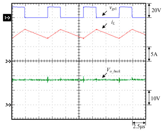
Figure 27.
Measured waveforms of the bidirectional buck converter in buck mode with a constant voltage of 16.8 V and an output current of 10 A: (1) vgs1; (2) iL; (3) Vo_buck.
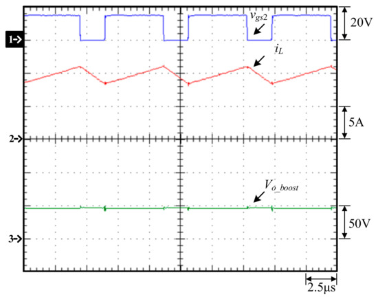
Figure 28.
Measured waveforms of the bidirectional buck converter in boost mode with an input voltage of 14.4 V and an output current of 3 A at a constant voltage of 48 V: (1) vgs2; (2) iL; (3) Vo_boos.
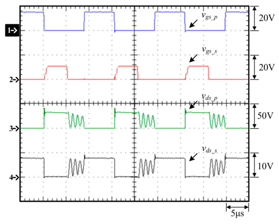
Figure 29.
Measured waveforms of the flyback converter with an input voltage of 14.4 V and an output voltage of 4.19 V at a constant current of 2 A: (1) vgs_p; (2) vgs_s; (3) vds_p; (4) vds_s.
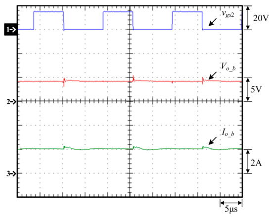
Figure 30.
Measured waveforms of the flyback converter with an input voltage of 14.4 V and an output voltage of 4.19 V at a constant current of 2 A: (1) vgs_p; (2) Vo_b; (3) Io_b.
6.5. Converter Efficiency Measurement
In this subsection, the efficiency measurement methods are shown in Figure 31, Figure 32, Figure 33 and Figure 34 for the different conditions of the main power stages. As shown in each figure, the digital meters are used to measure the input voltage, output voltage, and the voltage of the current-detecting resistor (Shunt) to obtain the input and output currents, which can be used to obtain the input power and output power, while the required load is regulated by a DC electronic load. Finally, the resulting input and output powers are used to calculate the efficiency of the actual circuit operation. Figure 35 shows the efficiency curve of the bidirectional buck converter in buck mode at a constant current. Figure 36 shows the efficiency curve of the bidirectional buck converter in buck mode at a constant voltage. Figure 37 shows the efficiency curve of the bidirectional buck converter in boost mode at a constant voltage. Figure 38 shows the efficiency curve of the flyback converter at a constant current.

Figure 31.
Block diagram for efficiency measurement of the bidirectional buck converter in buck mode at constant current.

Figure 32.
Block diagram for efficiency measurement of the bidirectional buck converter in buck mode at constant voltage.
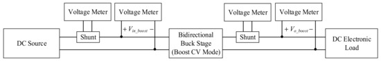
Figure 33.
Block diagram of efficiency measurement for the bidirectional buck converter in boost mode at constant voltage.
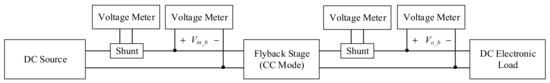
Figure 34.
Block diagram of efficiency measurement for the flyback converter at constant current.
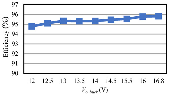
Figure 35.
Block diagram of efficiency measurement for the bidirectional buck converter in buck mode at a constant current of 10 A.
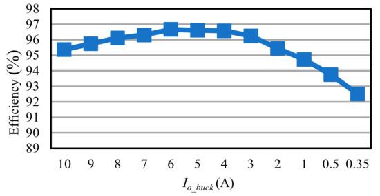
Figure 36.
Efficiency measurement for the bidirectional buck converter in buck mode at a constant voltage of 16.8 V.
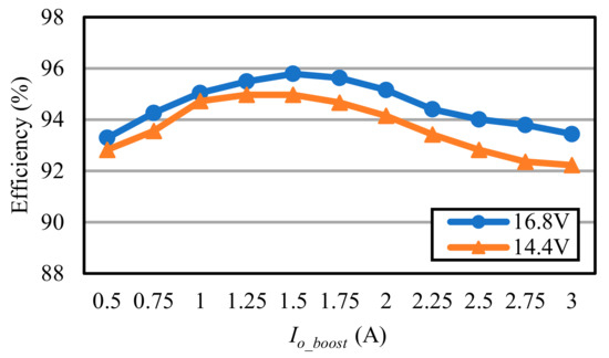
Figure 37.
Efficiency measurement for the bidirectional buck converter in boost mode at a constant voltage of 48 V.
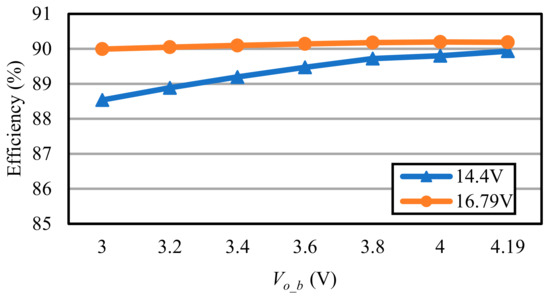
Figure 38.
Efficiency measurement for the flyback converter at a constant current of 2 A.
Figure 35 shows the efficiency curve of the bidirectional buck converter in buck mode at a constant current of 10 A. In Figure 35, the efficiency is above 94.25% and can be up to 95.82%. Figure 36 shows the efficiency curve of the bidirectional buck converter in buck mode at a constant voltage of 16.8 V. In Figure 36, as the output current decreases, the efficiency also decreases; the efficiency is above 92.51% and can be up to 96.67%. Figure 37 shows the efficiency curve of the bidirectional buck converter in boost mode at a constant voltage of 48 V. Figure 38 shows the efficiency curve of the bidirectional buck converter in boost mode at a constant voltage of 48 V. Comparing the two curves in Figure 38 with the input voltages of 16.8 V and 14.4 V, it can be seen that the efficiency decreases due to the increase in the input current because of the low input voltage, and the efficiency of the bidirectional buck converter is above 92.23% and can be up to 95.79%. Figure 38 shows the efficiency curve of the flyback converter at a constant current of 2 A. In Figure 38, due to the low output voltage range, the efficiency increases slightly when the output voltage is gradually increased, and the efficiency is above 88.54% and can be up to 90.25%.
7. Literature Comparison
The flyback converter was adopted as the circuit of the battery voltage equalizer in this study, and a comparison between our results and relevant studies in the literature was conducted.
Regarding charging balance, as shown in Table 6, the initial maximum and minimum battery voltages in [42] are 3.774 V and 3.464 V, respectively, with a battery voltage difference of 0.31 V, and the final maximum and minimum battery voltages are 3.871 V and 3.823 V, respectively, with the voltage difference between the maximum and minimum of 0.048 V after 140 min. The initial maximum and minimum battery voltages for the proposed control strategy are 3.507 V and 3.092 V, respectively, with the voltage difference between the maximum and minimum of 0.415 V, and the final maximum and minimum battery voltages proposed are 4.0 V and 3.993 V, respectively, with the voltage difference between the maximum and minimum of 0.007 V after 19.75 min. Therefore, from the comparison between the two, it can be seen that the proposed strategy has a higher initial battery voltage difference, shorter balancing time, and a smaller final battery voltage difference.
Table 6.
Comparison of charging balance.
Regarding discharge balance, as shown in Table 7, the initial maximum and minimum battery voltages in [42] are 4.027 V and 3.693 V, respectively, with the voltage difference between the maximum and minimum of 0.334 V. After 140 min, the final maximum and minimum battery voltages are 3.543 V and 3.494 V, respectively, with the voltage difference between the maximum and minimum of 0.049 V. The initial maximum and minimum battery voltages in [43] are 4.1 V and 3.99 V, respectively, with the voltage difference between the maximum and minimum of 0.11 V. Since this paper does not provide the detailed battery voltages, it is only known that the battery voltages are balanced at 3.99 V after 41.67 min. The initial maximum and minimum battery voltages for the proposed control strategy are 3.985 V and 3.566 V, respectively, with the voltage difference between the maximum and minimum of 0.419 V. After 24 min, the final maximum and minimum battery voltages are 3.338 V and 3.333 V, respectively, with the voltage difference between the maximum and minimum of 0.005 V. Therefore, from the comparison between the three, it can be seen that the proposed strategy has a higher initial battery voltage difference, shorter balancing time, and a smaller final battery voltage difference.
Table 7.
Comparison of discharging balance.
Regarding static balance, as shown in Table 8, the initial maximum and minimum values of the battery voltages in case 1 of [39] are 3.846 V and 3.79 V, respectively, with the voltage difference between the maximum and minimum of 0.056 V. Since this paper does not provide the detailed battery voltages, it is only known that the battery voltages are balanced at 3.84 V after 30 min. The initial maximum and minimum values of the battery voltages in case 2 of [39] are 3.86 V and 3.8 V, respectively, with the voltage difference between the maximum and minimum of 0.06 V. Since this paper does not provide the detailed battery voltages, it is only known the battery voltages are balanced at 3.84 V after 55 min. The initial maximum and minimum battery voltages are 3.756 V and 3.249 V, respectively, with the voltage difference between the maximum and minimum of 0.056 V. Since this paper does not provide the detailed battery voltages, it is only known that the final battery voltages are balanced at 4.04 V after 33.33 min. The initial maximum and minimum battery voltages for the proposed control strategy are 3.756 V and 3.249 V, respectively, with the voltage difference between the maximum and minimum of 0.507 V. After 20 min, the final maximum and minimum final battery voltages are 3.482 V and 3.475 V, respectively, with the voltage difference between the maximum and minimum of 0.007 V. Therefore, from the comparison between the three, it can be seen that the proposed control strategy has a higher initial battery voltage difference, shorter balancing time, and a smaller final battery voltage difference.
Table 8.
Comparison of static balance.
8. Conclusions
The chain-loop comparison strategy for battery voltage equalization based on the bidirectional buck converter and the flyback converter is presented. There are three modes, namely, charging balance, discharging balance, and static balance. The experimental results show that all three modes have the effect of battery voltage balancing. The voltage difference between the maximum and minimum is 0.007 V after a balancing time of 19.75 min, 0.005 V after a balancing time of 24 min, and 0.007 V after a balancing time of 20 min for charging balance, discharging balance, and static balance, respectively. The efficiency of the bidirectional buck converter is above 92.51% and up to 96.67% over the entire operating range, whereas the efficiency of the flyback converter is above 88.54% and up to 90.2% in this range. Accordingly, the effectiveness of the proposed chain-loop comparison strategy for active battery voltage balance can be verified by experiments and comparisons.
Author Contributions
Conceptualization, K.-I.H. and J.-J.S.; methodology, K.-I.H. and Y.-H.L.; software, Y.-H.L.; validation, Y.-H.L. and K.-I.H.; formal analysis, Y.-H.L. and J.-J.S.; investigation, Y.-H.L.; resources, K.-I.H.; data curation, Y.-H.L. and J.-J.S.; writing—original draft preparation, K.-I.H.; writing—review and editing, K.-I.H.; visualization, Y.-H.L. and J.-J.S.; supervision, K.-I.H.; project administration, K.-I.H.; funding acquisition, K.-I.H. All authors have read and agreed to the published version of the manuscript.
Funding
This research was funded by the Ministry of Science and Technology, Taiwan, under Grant Number NSTC 112-2221-E-027-015-MY2.
Data Availability Statement
The original contributions presented in the study are included in the article, further inquiries can be directed to the corresponding author.
Conflicts of Interest
Author Yuan-Hua Lin was employed by the company Monolithic Power System. The remaining authors declare that the research was conducted in the absence of any commercial or financial relationships that could be construed as a potential conflict of interest.
Abbreviations
| S1, S2 | Switches of bidirectional buck converter |
| Cboost | Output capacitance of bidirectional buck converter in boost mode |
| Cbuck | Output capacitance of buck mode of bidirectional buck converter |
| L | Inductance of bidirectional buck converter |
| Tb1, Tb2, Tb3, Tb4 | Coupling inductors of flyback converters |
| Sb1_p, Sb2_p, Sb3_p, Sb4_p | Primary switches of flyback converter |
| Sb1_s, Sb2_s, Sb3_s, Sb4_s | Secondary switches of flyback converters |
| Co_b1, Co_b2, Co_b3, Co_b4 | Output capacitances of flyback converters |
| Lm_b1, Lm_b2, Lm_b3, Lm_b4 | Magnetizing inductances of flyback converters |
| Np_b1, Np_b2, Np_b3, Np_b4 | Primary coils of flyback converters |
| Ns_b1, Ns_b2, Ns_b3, Ns_b4 | Primary coils of flyback converters |
| Vin_buck | Input voltage for buck mode of bidirectional buck converter |
| Vin_boost | Input voltage for boost mode of bidirectional buck converter |
| Vin_b | Input voltage for buck mode of bidirectional buck converter |
| Vo_buck | Output voltage for buck mode of bidirectional buck converter |
| Vo_boost | Output voltage for boost mode of bidirectional buck converter |
| Vo__b | Output voltage of flyback converter |
| Iin_buck | Input current for buck mode of bidirectional buck converter |
| Iin_boost | Input current for boost mode of bidirectional buck converter |
| Iin_b | Input current of flyback converter |
| iL | Current flowing through L |
| Io_buck | Output current for buck mode of bidirectional buck converter |
| Io_boost | Output current for boost mode of bidirectional buck converter |
| Io_b | Output current of flyback converter |
| Ro_boost | Output resistance for boost mode of bidirectional buck converter |
| iCbuck | Current in output capacitor Cbuck |
| iCboost | Current in output capacitor Cboost |
| vL | Voltage of inductor L |
| vLm_b | Voltage of magnetizing inductance Lm_b |
| vNp_b | Voltage of coil Np_b |
| vNs_b | Voltage of coil Ns_b |
| Coss1, Coss2, Coss_p | Parasitic output capacitances of S1, S2, Sb_s |
| vgs1, vgs2, vgs_p, vgs_s | Gate driving signals for switches S1, S2, Sb_s, Sb_p |
| vds1, vds2, vds_p, vds_s | Voltages of S1, S2, Sb_s, Sb_p |
| Dbuck | Duty cycle for buck mode of bidirectional buck converter |
| Ts1 | Switching period of flyback converter |
| Mbuck | Voltage conversion ratio for buck mode of bidirectional buck converter |
| Dboost | Duty cycle for boost mode of bidirectional buck converter |
| Mboost | Voltage conversion ratio for buck mode of bidirectional buck converter |
| Dx1 | On-time ratio of switch Sb_p |
| Dx2 | On-time ratio of switch Sb_s |
| Dx3 | Duration ratio of magnetizing inductance Lm_b when no energy is stored |
| Ts2 | Switching period of flyback converter |
| Mb | Voltage conversion ratio of the flyback converter |
| Ids_s_peak | Peak current in switch Sb_s |
| ILm_b_peak | Peak current in magnetizing inductor Lm_b |
| Ipack | Current in battery pack |
| Iin_bT | Total input current of flyback converter |
| Vb1, Vb2, Vb3, Vb4 | Voltages of battery cell |
| Ib1_T, Ib2_T, Ib3_T, Ib4_T | Currents in battery cell |
References
- Lu, L.; Han, X.; Li, J.; Hua, J.; Ouyang, M. A review on the key issues for lithium-ion battery management in electric vehicles. J. Power Sources 2013, 226, 272–288. [Google Scholar] [CrossRef]
- Uno, M.; Tanaka, K. Accelerated charge-discharge cycling test and cycle life prediction model for super capacitors in alternative battery applications. IEEE Trans. Ind. Electron. 2012, 59, 4704–4712. [Google Scholar] [CrossRef]
- Park, H.; Kim, C.; Park, K.; Moon, G.; Lee, J. Design of a charge equalizer based on battery modularization. IEEE Trans. Veh. Technol. 2009, 58, 3216–3223. [Google Scholar] [CrossRef]
- Kim, J.; Shin, J.; Chun, C.; Cho, B.H. Stable configuration of a Li-ion series battery pack based on a screening process for improved voltage/SOC balancing. IEEE Trans. Power Electron. 2021, 27, 411–424. [Google Scholar] [CrossRef]
- Kelkar, A.; Dasari, Y.; Williamson, S.S. A comprehensive review of power electronics enabled active battery cell balancing for smart energy management. In Proceedings of the IEEE International Conference on Power Electronics, Smart Grid and Renewable Energy (PESGRE), Cochin, India, 2–4 January 2020; pp. 1–6. [Google Scholar]
- Rui, L.; Lizhi, W.; Xueli, H.; Qiang, D.; Jie, Z. A review of equalization topologies for lithium-ion battery packs. In Proceedings of the IEEE 34th Chinese Control Conference, Hangzhou, China, 28–30 July 2015; pp. 7922–7927. [Google Scholar]
- Daowd, M.; Omar, N.; Bossche, P.V.; Mierlo, J.V. A review of passive and active battery balancing based on MATLAB Simulink. Int. Rev. Electr. Eng. 2011, 6, 2974–2989. [Google Scholar]
- Ghaeminezhad, N.; Ouyang, Q.; Hu, X.; Xu, G.; Wang, Z. Active cell equalization topologies analysis for battery packs: A systematic review. IEEE Trans. Power Electron. 2021, 36, 9119–9135. [Google Scholar] [CrossRef]
- Cao, J.; Schofield, N.; Emadi, A. Battery balancing methods: A comprehensive review. In Proceedings of the IEEE Vehicle Power and Propulsion Conference (VPPC), Harbin, China, 3–5 September 2008; pp. 1–6. [Google Scholar]
- Daowd, M.; Omar, N.; Van Den Bossche, P.; Van Mierlo, J. Passive and active battery balancing comparison based on matlab simulation. In Proceedings of the IEEE Vehicle Power and Propulsion Conference (VPPC), Chicago, IL, USA, 6–9 September 2011; pp. 1–7. [Google Scholar]
- Ci, S.; Lin, N.; Wu, D. Reconfigurable battery techniques and systems: A survey. IEEE Access 2016, 4, 1175–1189. [Google Scholar] [CrossRef]
- Omariba, Z.B.; Zhang, L.; Sun, D. Review of battery cell balancing methodologies for optimizing battery pack performance in electric vehicles. IEEE Access 2019, 7, 129335–129352. [Google Scholar] [CrossRef]
- Qi, J.; Dah-Chuan Lu, D. Review of battery cell balancing techniques. In Proceedings of the Australasian Universities Power Engineering Conference (AUPEC), Perth, WA, Australia, 28 September–1 October 2014; pp. 1–6. [Google Scholar]
- Vardwaj, V.; Vishakha, V.; Jadoun, V.K.; Jayalaksmi, N.S.; Agarwal, A. Various methods used for battery balancing in electric vehicles: A comprehensive review. In Proceedings of the IEEE International Conference on Power Electronics & IoT Applications in Renewable Energy and Its Control (PARC), Mathura, India, 28–29 February 2020; pp. 208–213. [Google Scholar]
- Phung, T.H.; Crebier, J.C.; Lembeye, Y. Voltage balancing converter network for series-connected battery stack. In Proceedings of the IEEE Conference on Industrial Electronics Society (IECON), Montreal, QC, Canada, 25–28 October 2012; pp. 3007–3013. [Google Scholar]
- Lindemark, B. Individual cell voltage equalizers (ICE) for reliable battery performance. In Proceedings of the IEEE International Telecommunications Energy Conference (INTELEC), Kyoto, Japan, 5–8 November 1991; pp. 196–201. [Google Scholar]
- Wei, L.; Jie, L.; Wenji, S.; Ziping, F. Study on passive balancing characteristics of serially connected lithium-ion battery string. In Proceedings of the IEEE International Conference on Electronic Measurement & Instruments (ICEMI), Yangzhou, China, 20–22 October 2017; pp. 489–495. [Google Scholar]
- Du, J.; Wang, Y.; Tripathi, A.; Lam, J.S.L. Li-ion battery cell equalization by modules with chain structure switched capacitors. In Proceedings of the IEEE Asian Conference on Energy, Power and Transportation Electrification (ACEPT), Singapore, 25–26 October 2016; pp. 1–6. [Google Scholar]
- Mahardiono, N.A.; Setiawan, D.; Purnama, I. A study on transfer element in single switched capacitor battery balancer system. In Proceedings of the International Conference on Sustainable Energy Engineering and Application (ICSEEA), Tangerang, Indonesia, 1–2 November 2018; pp. 64–68. [Google Scholar]
- Moral, C.G.; Laborda, D.F.; Alonso, L.S.; Guerrero, J.M.; Fernandez, D.; Pereda, C.R.; Reigosa, D.D. Battery internal resistance estimation using a battery balancing system based on switched capacitors. IEEE Trans. Ind. Appl. 2020, 56, 5363–5374. [Google Scholar] [CrossRef]
- Shang, Y.; Xia, B.; Yang, J.; Zhang, C.; Cui, N.; Mi, C. A delta-structured switched-capacitor equalizer for series-connected battery strings. In Proceedings of the IEEE Energy Conversion Congress and Exposition (ECCE), Cincinnati, OH, USA, 1–5 October 2017; pp. 4493–4496. [Google Scholar]
- Shang, Y.; Zhang, Q.; Cui, N.; Duan, B.; Zhang, C. An optimized mesh-structured switched-capacitor equalizer for lithium-ion battery strings. IEEE Trans. Transp. Electrif. 2019, 5, 252–261. [Google Scholar] [CrossRef]
- Ye, Y.; Cheng, K.W.E.; Fong, Y.C.; Xue, X.; Lin, J. Topology, modeling, and design of switched-capacitor-based cell balancing systems and their balancing exploration. IEEE Trans. Power Electron. 2017, 32, 4444–4454. [Google Scholar] [CrossRef]
- Singh, H.R.; Pandey, K.; Prakash, A. Active cell balancing using microcontroller. In Proceedings of the IEEE International Conference on Power Energy, Environment and Intelligent Control (PEEIC), Greater Noida, India, 13–14 April 2018; pp. 82–84. [Google Scholar]
- Moghaddam, A.F.; Van Den Bossche, A. An active cell equalization technique for lithium-ion batteries based on inductor balancing. In Proceedings of the IEEE International Conference on Mechanical and Aerospace Engineering (ICMAE), Budapest, Hungary, 10–13 July 2018; pp. 274–278. [Google Scholar]
- Wang, S.; Yang, S.; Yang, W.; Wang, Y. A new kind of balancing circuit with multiple equalization modes for serially connected battery pack. IEEE Trans. Ind. Electron. 2021, 68, 2142–2150. [Google Scholar] [CrossRef]
- Cao, X.; Zhong, Q.-C.; Qiao, Y.-C.; Deng, Z.-Q. Multilayer modular balancing strategy for individual cells in a battery pack. IEEE Trans. Energy Convers. 2018, 33, 526–536. [Google Scholar] [CrossRef]
- Narayanaswamy, S.; Steinhorst, S.; Lukasiewycz, M.; Kauer, M.; Chakraborty, S. Optimal dimensioning and control of active cell balancing architectures. IEEE Trans. Veh. Technol. 2019, 68, 9632–9646. [Google Scholar] [CrossRef]
- Ouyang, Q.; Chen, J.; Zheng, J.; Hong, Y. SOC estimation-based quasi-sliding mode control for cell balancing in lithium-ion battery packs. IEEE Trans. Ind. Electron. 2018, 65, 3427–3436. [Google Scholar] [CrossRef]
- Imtiaz, A.M.; Khan, F.H. Time shared flyback converter based regenerative cell balancing technique for series connected li-ion battery strings. IEEE Trans. Power Electron. 2013, 28, 5960–5975. [Google Scholar] [CrossRef]
- Lim, C.; Lee, K.; Ku, N.; Hyun, D.; Kim, R. A modularized equalization method based on magnetizing energy for a series-connected lithium-ion battery string. IEEE Trans. Power Electron. 2014, 29, 1791–1799. [Google Scholar] [CrossRef]
- Narayanaswamy, S.; Kauer, M.; Steinhorst, S.; Lukasiewycz, M.; Chakraborty, S. Modular active charge balancing for scalable battery packs. IEEE Trans. Very Large Scale Integr. Syst. 2017, 25, 974–987. [Google Scholar] [CrossRef]
- Peng, F.; Wang, H.; Yu, L. Analysis and design considerations of efficiency enhanced hierarchical battery equalizer based on bipolar CCM buck-boost units. IEEE Trans. Ind. Appl. 2019, 55, 4053–4063. [Google Scholar] [CrossRef]
- Shang, Y.; Cui, N.; Duan, B.; Zhang, C. A global modular equalizer based on forward conversion for series-connected battery strings. IEEE J. Emerg. Sel. Top. Power Electron. 2018, 6, 1456–1469. [Google Scholar] [CrossRef]
- Ouyang, Q.; Han, W.; Zou, C.; Xu, G.; Wang, Z. Cell balancing control for lithium-ion battery packs: A hierarchical optimal approach. IEEE Trans. Ind. Inform. 2020, 16, 5065–5075. [Google Scholar] [CrossRef]
- Han, W.; Zou, C.; Zhou, C.; Zhang, L. Estimation of cell SOC evolution and system performance in module-based battery charge equalization systems. IEEE Trans. Smart Grid 2019, 10, 4717–4728. [Google Scholar] [CrossRef]
- Liu, K.; Yang, Z.; Tang, X.; Cao, W. Automotive battery equalizers based on joint switched-capacitor and buck-boost converters. IEEE Trans. Veh. Technol. 2020, 69, 12716–12724. [Google Scholar] [CrossRef]
- Zhou, G.; Zhang, X.; Gao, K.; Tian, Q.; Xu, S. Two-mode active balancing circuit based on switched-capacitor and three-resonant-state LC units for series-connected cell strings. IEEE Trans. Ind. Electron. 2022, 69, 4845–4858. [Google Scholar] [CrossRef]
- Nazi, H.; Babaei, E. A modularized bidirectional charge equalizer for series-connected cell strings. IEEE Trans. Ind. Electron. 2021, 68, 6739–6749. [Google Scholar] [CrossRef]
- Chang, C.-H.; Cheng, C.-A.; Chang, E.-C.; Cheng, H.-L.; Yang, B.-E. An integrated high-power-factor converter with ZVS transition. IEEE Trans. Power Electron. 2016, 31, 2326–2371. [Google Scholar] [CrossRef]
- Raeber, M.; Heinzelmann, A.; Abdeslam, D.O. Analysis of an active charge balancing method based on a single nonisolated DC/DC converter. IEEE Trans. Ind. Electron. 2021, 68, 2257–2265. [Google Scholar] [CrossRef]
- Guo, X.; Geng, J.; Liu, Z.; Xu, X.; Cao, W. A flyback converter-based hybrid balancing method for series-connected battery pack in electric vehicles. IEEE Trans. Veh. Technol. 2021, 70, 6626–6635. [Google Scholar] [CrossRef]
- Yang, Y.; Hu, K.; Tsai, C. Digital battery management design for point-of-load applications with cell balancing. IEEE Trans. Ind. Electron. 2020, 67, 6365–6375. [Google Scholar] [CrossRef]
- Xie, D.; Lin, C.; Deng, Q.; Lin, H.; Cai, C.; Basler, T.; Ge, X. Simple vector calculation and constraint-based fault-tolerant control for a single-phase CHBMC. IEEE Trans. Power Electron. 2024. early access. [Google Scholar] [CrossRef]
Disclaimer/Publisher’s Note: The statements, opinions and data contained in all publications are solely those of the individual author(s) and contributor(s) and not of MDPI and/or the editor(s). MDPI and/or the editor(s) disclaim responsibility for any injury to people or property resulting from any ideas, methods, instructions or products referred to in the content. |
© 2024 by the authors. Licensee MDPI, Basel, Switzerland. This article is an open access article distributed under the terms and conditions of the Creative Commons Attribution (CC BY) license (https://creativecommons.org/licenses/by/4.0/).