Review

A Review on the Recent Development of High-Frequency Inverters for Wireless Power Transfer

by
Ying Liu
1,2,
Liangyi Pan
1,
Shunyu Yao
1,2,
Jiantao Zhang
1,2,*,
Shumei Cui
1,2 and
Chunbo Zhu
1,2
1
School of Electric Engineering and Automation, Harbin Institute of Technology, Harbin 150001, China
2
Zhengzhou Research Institute, Harbin Institute of Technology, Zhengzhou 450003, China
*
Author to whom correspondence should be addressed.
Energies 2024, 17(20), 5153; https://doi.org/10.3390/en17205153
Submission received: 20 September 2024 / Revised: 13 October 2024 / Accepted: 14 October 2024 / Published: 16 October 2024
(This article belongs to the Section F1: Electrical Power System)

Abstract

:
With the demand for the miniaturization and integration of wireless power transfer (WPT) systems, higher frequency is gradually becoming the trend; thus, the power electronic device has become one of the main reasons for limiting the development. Therefore, further research on high-frequency inverters and purposeful design according to the characteristics of WPT systems are of great significance to promote the development of high-frequency WPT technology. There is still no literature that summarizes all the inverter circuits that can be applied to WPT systems, which makes it extremely difficult to find an inverter that meets the designer’s requirements. This paper reviews the high-frequency inverters for WPT systems, summarizes the derived topologies based on power amplifiers and H-bridge inverters, investigates the main factors restricting the development of high-frequency inverters, and analyzes the research directions for future development.

1. Introduction

In recent years, with the development of technology and the progress of society, wireless power transfer (WPT) technology began to appear in various aspects of people’s lives. WPT technology is a comprehensive application of power electronics, electric technology, control theory, and many other subjects, using magnetic field, electric field, microwave and other carriers to realize the transmission of power from the source side to the equipment in a non-contact way [1,2,3,4,5]. This technology realizes the convenient and safe connection of power supply and removes the problems of limited equipment flexibility and safety hazards caused by the traditional wired power transfer method, and its application area involves a variety of fields such as electric vehicles, biomedical instrument, underwater equipment, etc. [6,7,8,9,10].
The near-field wireless power transfer includes inductive power transfer (IPT) that utilizes magnetic field to transfer power and capacitive power transfer (CPT) that utilizes electric field to transfer power; the system structure is shown in Figure 1 [11].
Conventional IPT and CPT systems operating at kHz frequency require external capacitors or inductors with larger capacity to compensate the couplers, and WPT systems are showing a trend towards higher MHz level frequency due to the user demand for integration and miniaturization of power transmission devices [12]. Current research on WPT technology mainly focuses on couplers, compensation networks, and system modeling, with relatively little attention paid to the inverter part. However, the development trend of a higher frequency puts more rigorous requirements on the design of inverters, which will face challenges such as high switching loss, the influence of parasitic elements, and high driving loss [13]. However, a detailed review on inverters for WPT systems is still lacking. Therefore, it is of great significance to conduct a review and study of inverter circuits for WPT systems for promoting the development of high-frequency WPT technologies.
The main high-frequency inverters used in WPT systems are oscillators, power amplifiers, and topologies based on H-bridge inverters, as shown in Figure 2. Oscillators are circuits that utilize the charging and discharging phenomenon of capacitors and inductors to produce an oscillating alternating current. Oscillator circuits for high-frequency power supplies can be divided into Hartley oscillators, Colpitts Oscillators, and so on. This type of inverter has a simple circuit structure and high oscillation frequency. Earlier MIT research used a Colpitts Oscillator circuit as the inverter for the WPT system [14], and the system efficiency was only 40% when the coil transfer efficiency achieved 90%. The Hartley oscillator circuit contains many high harmonics of the signal, and the frequency of the Colpitts Oscillator is not easy to control, so it is less used in the WPT system at present. Power amplifiers are devices that amplify an input signal to produce a high-power output to drive a load under a given distortion rate and can be categorized into linear amplifiers and switching amplifiers according to the different modes of operation. Due to the high loss of linear amplifiers such as Class-A and Class-B, the resonant power amplifiers currently used in WPT systems are switching amplifiers such as Class-D, Class-E, Class-EF, etc., which are mainly oriented to applications above MHz and are limited in power level due to the constraints of switching device stress. The H-bridge inverter circuit consists of four MOSFETs in two bridge arms, which can be used to convert a DC power supply to an AC output by adjusting the turn-on and turn-off of the switches with the appropriate switching sequence. Currently, the most widely used inverters in high-power WPT systems are H-bridge Inverters, and various types of new topologies have been derived depending on the application requirements. In addition, for high-frequency applications, the distribution of parasitic parameters in the circuits and their effects also need to be paid attention to.
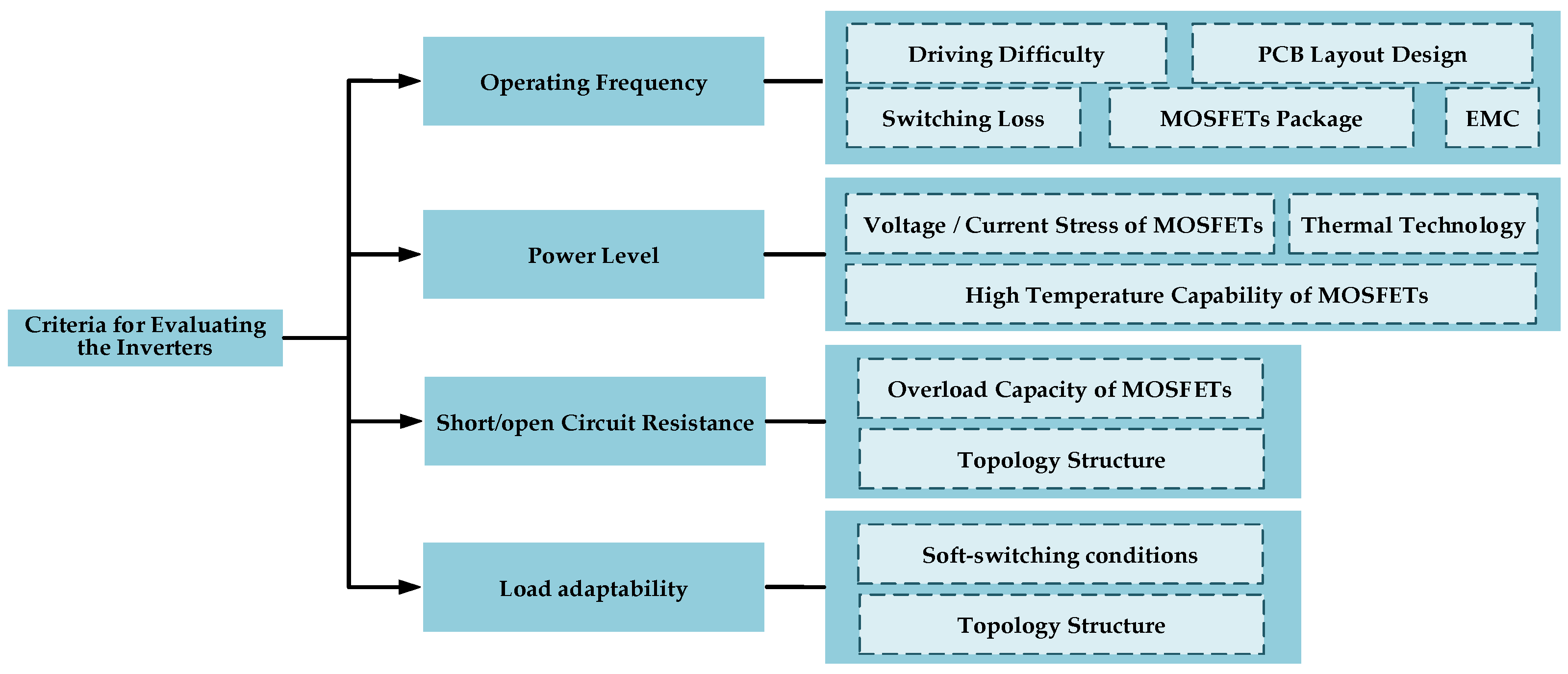
The criteria for evaluating high-frequency inverters in WPT systems can include operating frequency, power level, short/open circuit resistance, load adaptability, etc., as shown in Figure 3. Among them, the operating frequency that an inverter can achieve is mainly limited by switching losses, PCB layout design, driving difficulty, Electromagnetic Compatibility (EMC) and MOSFETs’ packaging. These limitations are closely related to the topology, inverter topologies with simple structures and fewer MOSFETs tend to operate at higher frequencies. The power level of the inverter is then determined by the voltage/current stress of the MOSFETs, the heat resistance of the MOSFETs, and the heat dissipation technology. Inverters with a large number of MOSFETs tend to share the voltage/current stress and spread the heat generation, so the operating frequency and power level of the inverter are always constrained by each other. Short/open circuit resistance and load adaptability are particular requirements that WPT systems put on inverters. In general, voltage-type inverters have better open-circuit resistance, current-type inverters have better short-circuit resistance; load adaptability is determined by the soft-switching conditions of each type of topologies. When selecting an inverter for a WPT system, the above evaluation criteria should be synthesized according to the specific requirements of the system, and the inverter topology that is compatible with the specific WPT should be selected.
The main objective of this paper is to summarize the current topologies and related technologies of high-frequency inverters for WPT systems and to study the key issues in high-frequency inverters. In Section 2 and Section 3, power amplifier circuits, topologies based on H-bridge inverters, are introduced. Section 4 analyzes the problems faced by inverters under high-frequency operating conditions and some current solutions. Finally, future research directions and key issues are discussed in Section 5 and the conclusion of the paper is given in Section Section 6.

2. Inverters Based on Power Amplifiers

The basic power amplifiers can be divided into Class-A, Class-B, Class-AB, Class-C, Class-D, Class-E, Class-DE and Class-F. Class-A power amplifier with a maximum efficiency of 25%, suitable for amplification of amplitude, single-sideband amplitude modulation applications; Class-B power amplifier with a theoretical efficiency of 75%, realize the push-pull work, but prone to crossover distortion, mainly used for the amplification of baseband signals; Class-AB power amplifier combines the advantages of Class-A and Class-AB amplifiers, but the efficiency is low, only suitable for amplification of audio signals; Class-C power amplifier, although having an efficiency of up to 80%, have a high level of distortion and are only suitable for applications in weak areas such as frequency multiplier. These four types of power amplifiers belong to linear power amplifiers, due to the switching devices working in the linear amplification area, the loss is large and is not suitable for use as an inverter in a WPT system.
In linear power amplifiers, most of the losses in the power transistor occur in the conduction phase. At this stage, both high voltage and high current are present on the switches, resulting in large losses on the switches. Switching mode power amplifiers such as Class-D, Class-E, Class-DE and Class-F can stagger the time of the emergence of large voltages and large currents on the switches, i.e., there is only a large current when the switch is on and the voltage is very small, and there is only a large voltage when the switch is off and there is no current flow, which can greatly reduce the loss on switching devices.
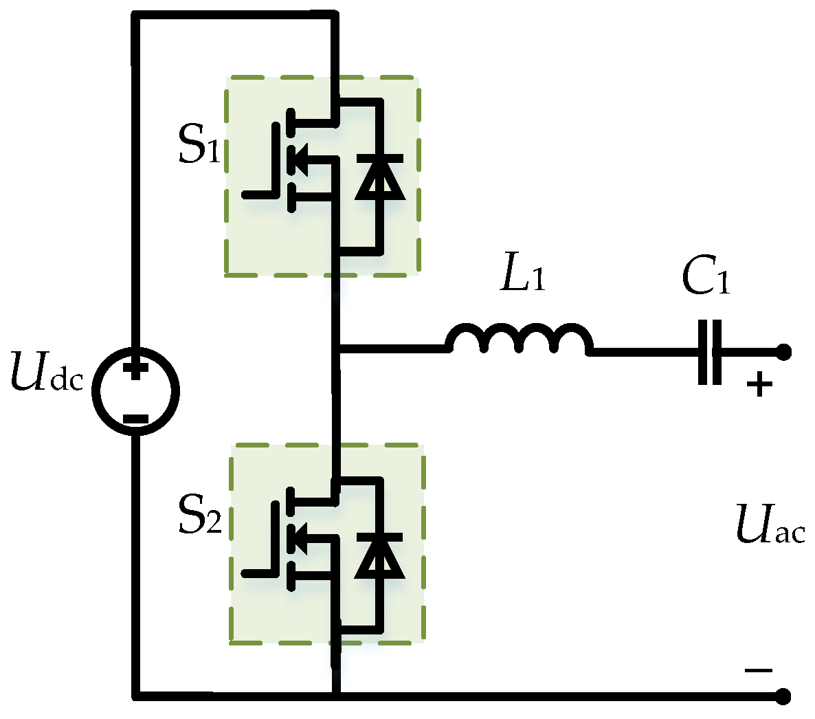
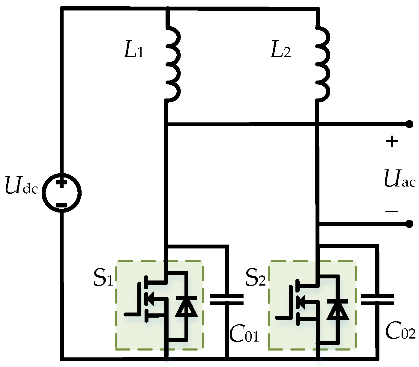
The structure of Class-D power amplifier is shown in Figure 4, where two MOSFETs are connected in series with the power source and take turns to conduct under the control signal and, thus, generating a square-wave voltage at the midpoint of the bridge. Due to the presence of a series resonant loop, a sine-wave output current is generated. Since both MOSFETs are operating in the switching state, they do not produce significant power dissipation. Class-D power amplifiers are now widely used in small and medium power WPT systems [15,16,17,18,19,20]. However, since the output voltage of the Class-D power amplifier contains DC components, the compensation topology is required to have good isolation characteristics in order to avoid generating large DC bias currents at the transmitter side of the WPT systems that can adversely affect the system. Wang, Y. et al. designed a highly robust WPT system based on a Class-D power amplifier and used a CLC compensation topology at the primary side to better isolate the DC voltage from the Class-D power amplifier [21]. In response to the high efficiency requirements of WPT systems, Ge, X. et al. proposed a discontinuous conduction mode (DCM) zero-voltage switching (ZVS) scheme for Class-D power amplifiers, which further improves the system efficiency [22].
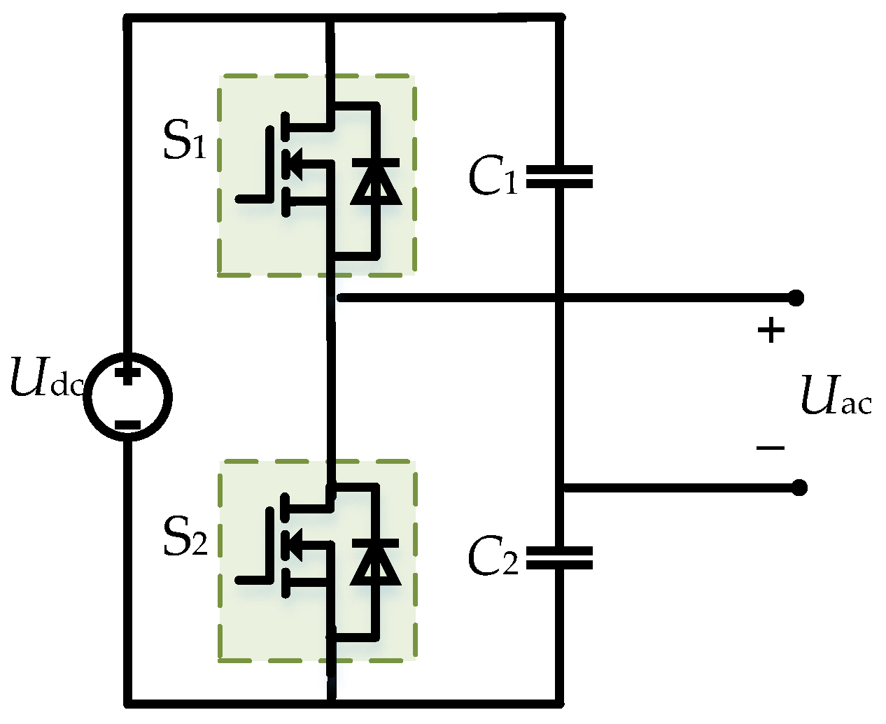
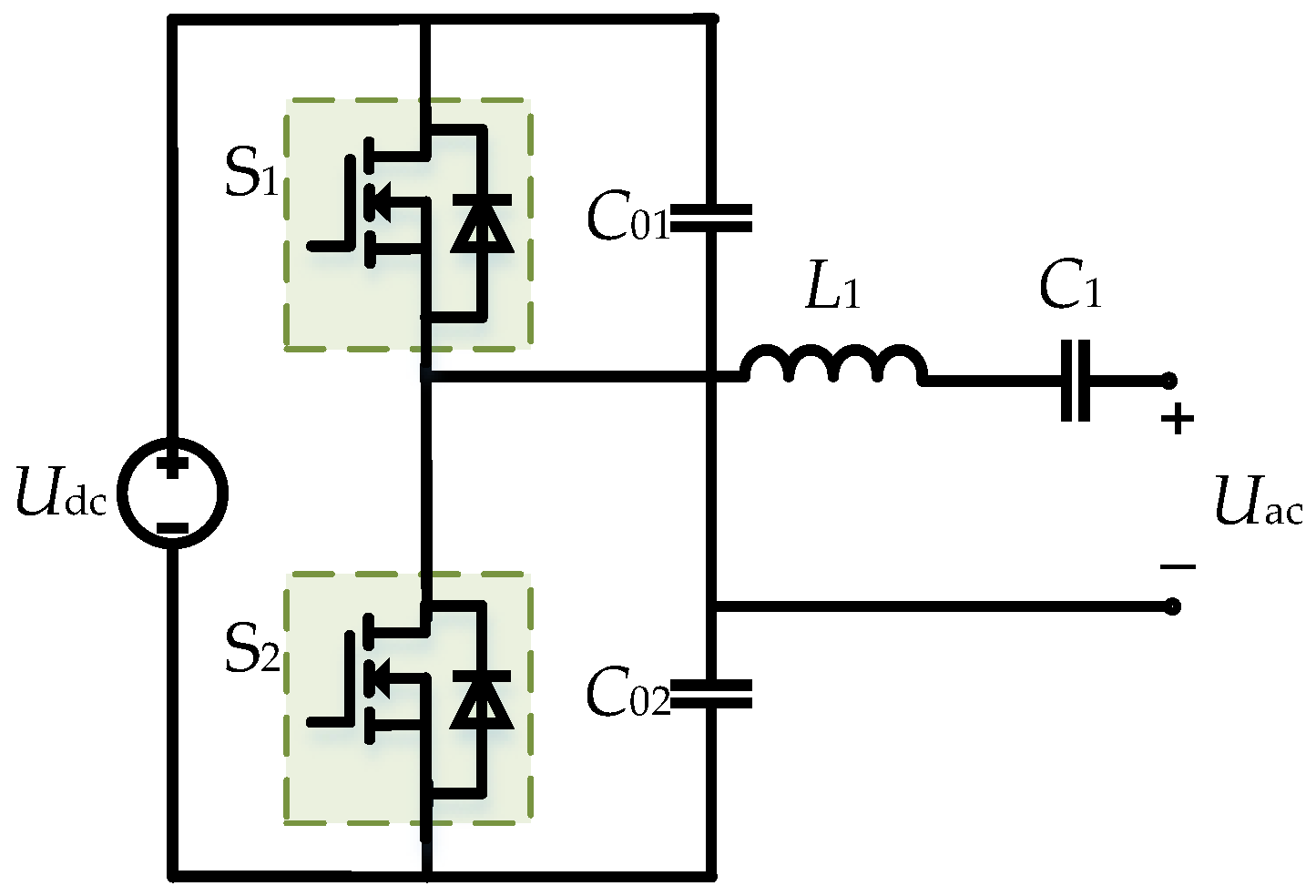
In order to reduce the limitations on the compensation topology caused by the Class-D power amplifier, a number of WPT systems use a mid-point clamped Class-D power amplifier as shown in Figure 5, which is also known as the half-bridge inverter [23,24,25,26]. This structure can effectively eliminate the DC component and even harmonics of the output voltage. With this no longer being a requirement for the isolation capability of the compensation topology, the design of the WPT system becomes more flexible. However, the power density of the inverter is reduced due to the addition of two bulky capacitors for power storage, and the problem of capacitor voltage equalization is introduced.
Due to the two MOSFETs on one bridge arm, it is necessary for the high and low side MOSFETs to work together and reasonably set the dead time to prevent the bridge arm from going directly through, and the switching speed of the device restricts the operating frequency of the Class-D power amplifier. Because of the floating voltage at the midpoint of the bridge arm, the high side driver of the MOSFET needs bootstrap booster circuit or independent power supply, resulting in a complex driving circuit.
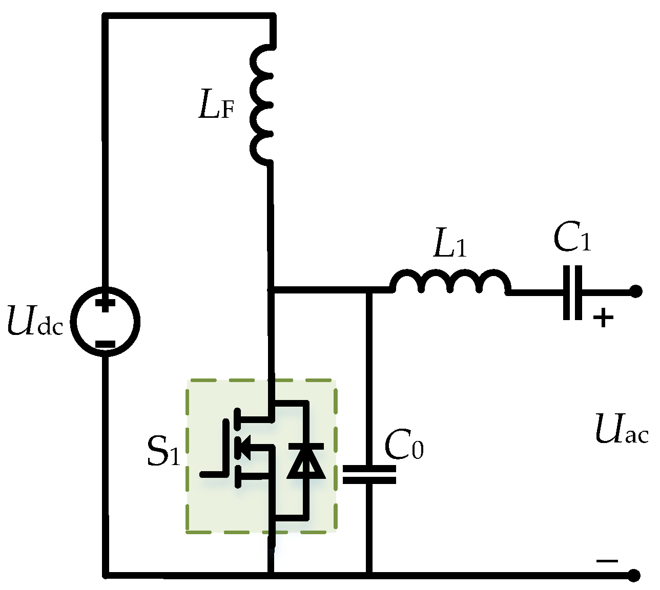
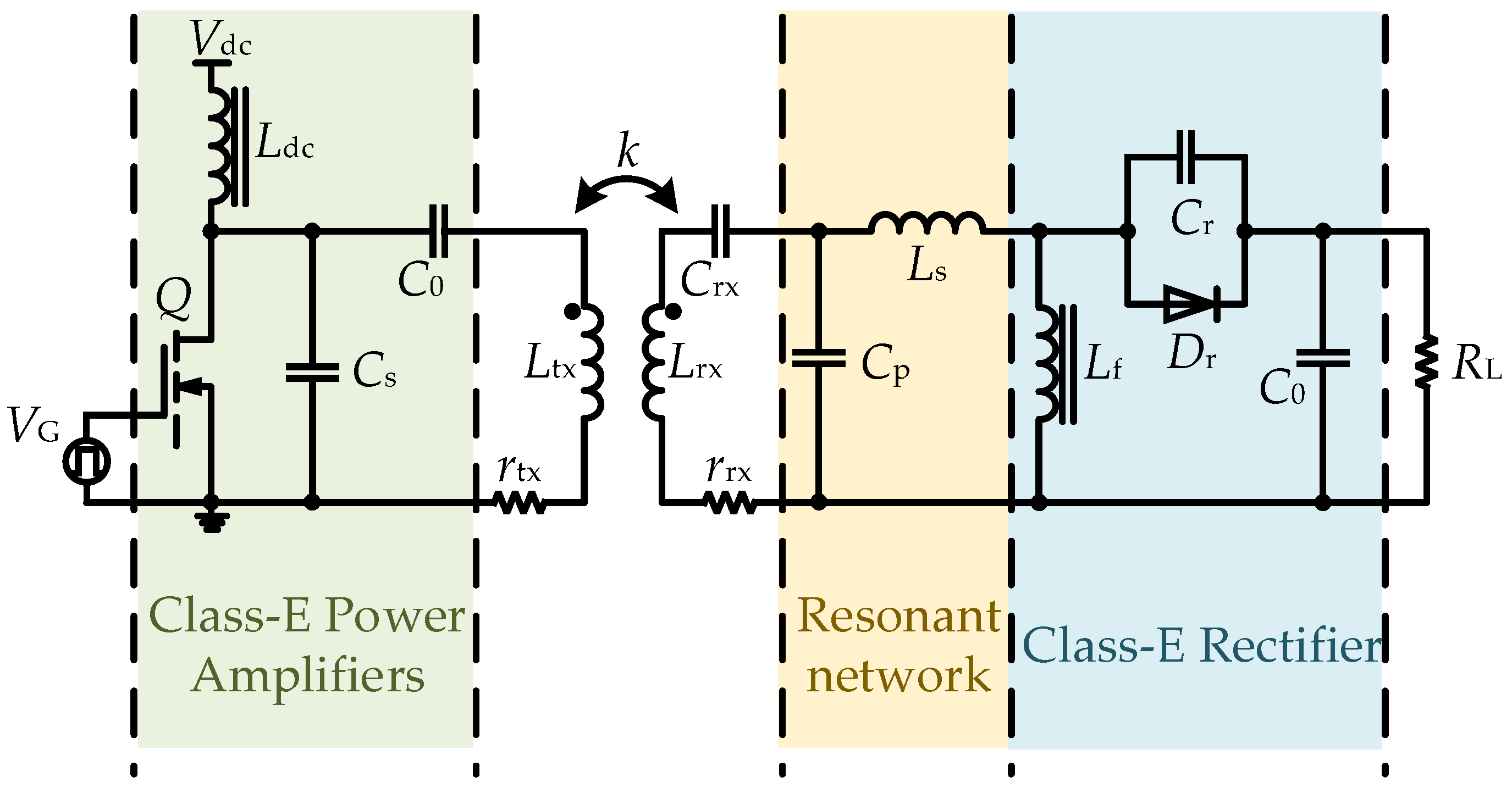
The structure of the Class-E power amplifier is shown in Figure 6, which is the major choice for the current high-frequency low-power WPT systems above MHz, due to the fact that the topology contains only one MOSFET, which is easy to drive, and has zero voltage switching (ZVS) and zero voltage derivative switching (ZVDS) with theoretical efficiency close to 100% [27,28,29,30,31,32,33,34]. However, the peak voltage across the MOSFET of Class-E power amplifiers is 3.6 times that of the input DC voltage, and due to the limitations of MOSFET withstand values they cannot operate at a higher voltage, and the maximum power achieved by Class-E power amplifiers is currently only 1 kW [35].
To improve the power of the Class-E power amplifier, a double Class-E inverter is proposed [5], as shown in Figure 7. The double Class-E power amplifier consists of two MOSFETs that conduct alternately and can be shared to withstand voltage stresses. Compared to Class-E power amplifiers, the double Class-E amplifiers can achieve four times as much power with the same MOSFET voltage stress and still have the advantages of Class-E power amplifiers, such as high efficiency and the possibility of soft-switching. However, the system complexity increases due to the addition of switching devices.
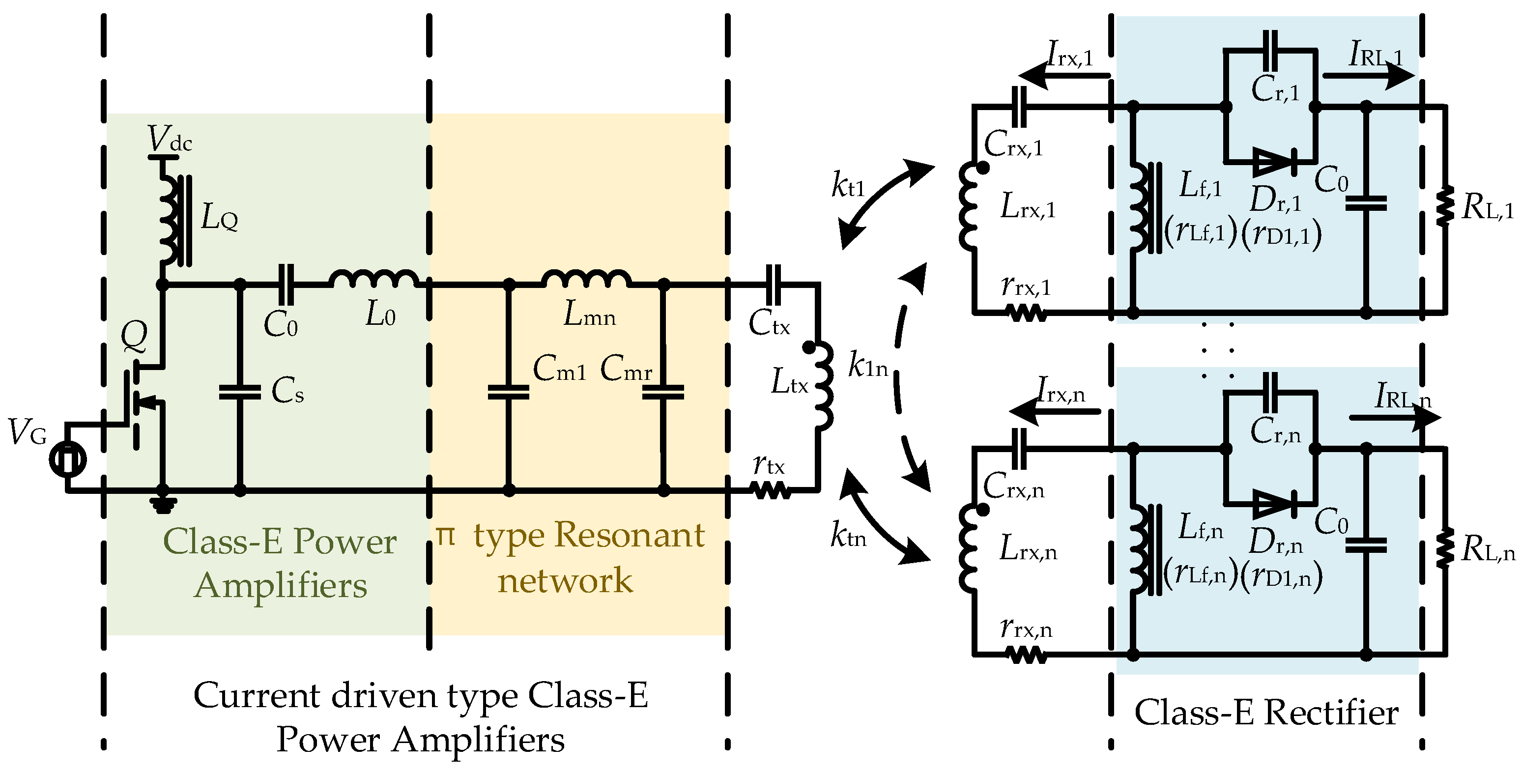
In addition, the best ZVS operation of Class-E power amplifiers depends on the load conditions and requires high resonance accuracy and, thus, making them more sensitive to changes in resonant circuit parameters. When the Class-E power amplifier is applied to the WPT system, the offset of the coupler (distance change, angular misalignment, etc.) will cause the change in the input impedance, and when the load of the Class-E power amplifier deviates from the optimum value, the efficiency will drop rapidly. In order to improve the performance of the WPT system in dynamic conditions, the circuit can be adaptively adjusted or controlled by frequency tracking, adding a DC–DC converter control after the rectifier, and so on [36]. This approach requires relatively complex control algorithms as well as hardware circuits dedicated to measurement, communication, computation, and implementation of control functions, increasing the complexity of the system. Adding a static matching network is a simpler measure. Song J. et al. add a π-type impedance matching network between the Class-E amplifier and the transmitting coil, as shown in Figure 8, which realizes the current-source function of the inverter and improves its loading conditions by means of the π-type impedance transforming network and the load traction technique [37]. Liu M et al. improved the loading conditions of the coupler and Class-E power amplifier by adding an L-type impedance matching network on the receiving side of the WPT system, as shown in Figure 9, which improved the freedom of the system [38].
The Class-DE power amplifier, shown in Figure 10, has the characteristics of both Class-D and Class-E power amplifiers, i.e., the ZVS and ZVDS conditions of Class-E are applied to the Class-D power amplifier. Compared to Class-E power amplifiers, it is easier to realize high power applications because the voltage of the MOSFET is only DC voltage. Compared to Class-D power amplifiers, it has higher efficiency due to the realization of MOSFET ZVS and ZVDS [39].
The input–output transfer function of the Class-DE is shown in Equation (1), which can easily adjust the voltage gain, and with a good control strategy, the Class-DE power amplifier can realize a good performance of the WPT system.
G ( s ) = Z L L 1 s s 2 + Z L L 1 s + 1 L 1 C 1
Nikiforidis, I et al. applied Class-DE power amplifiers to the WPT system, together with third-generation wide-bandwidth semiconductor devices, achieving a 3.39 MHz, 3 kW power transfer with a peak efficiency of 95% [40]. Aviles J.P.O. et al. designed an auto-regressive exogenous output (ARX) model Class-DE power amplifier based on an adaptive linear neuron (ADALINE) network to provide WPT systems with the ability to adapt to the stabilized outputs under different coupler offsets, which further broadens the range of applications of Class-DE power amplifiers [41].
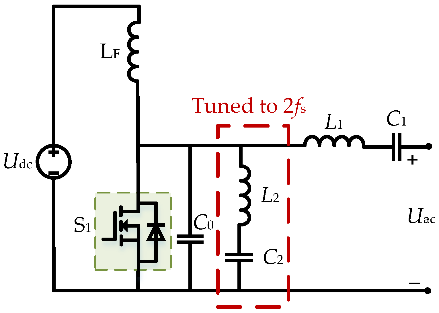
Class F power amplifiers use LC resonant tanks to control the harmonic content of the output voltage or current, which is the oldest technique to improve the efficiency of RF power amplifiers [42]. It is often used in combination with Class-E power amplifiers in WPT systems, where an LC resonant network is connected in parallel with a Class-E power amplifier to form a Class-EFn power amplifier, where n indicates the number of harmonics suppressed. Class-E power amplifiers contain strong second harmonic components, which may make it difficult for WPT systems to meet EMI requirements, so the most widely used is the Class-EF2 power amplifier, which is also known as the Class-Φ2 power amplifier [43], as shown in Figure 11.
Samer, A et al. designed a WPT system incorporating Class-EF2 inverter and Class-EF2 rectifier topologies and experimentally verified that the system using Class-EF2 topology has a higher efficiency than that of using Class-E power amplifiers in practical applications [44]. In addition, the peak voltage of the MOSFETs of Class-EF2 power amplifiers is only 2.2 times of the input DC voltage, making them attractive for high-power applications. J. Choi et al. have achieved a 2 kW single Class-EF2 power amplifier at 13.56 MHz [45] and a push–pull stage Class-EF2 power amplifier with an output power of 2.2 kW at 6.78 MHz [46].
A high-frequency inverter circuit is a combination of a low-frequency power inverter circuit and RF power amplifier circuit, so, drawing on various types of switching mode power amplifiers in RF circuits to be applied to the WPT system is a very sensible choice. A solid foundation has been laid for the high frequency of WPT technology, and a comparison of the performance of the above types of power amplifiers is shown in Table 1.

3. Inverters Based on H-Bridge

Full-bridge inverters, also known as H-bridge inverters, are the most commonly used inverter circuits in medium and high power systems and can be categorized into voltage-type inverter and current type inverter according to the input power source, as shown in Figure 12.
The voltage-type H-bridge inverter has a stabilized DC voltage as input and a square-wave voltage as output, which has the advantages of simple control strategy, easy realization of soft switching, high efficiency and high-power density [47,48,49,50]. It has been widely used in medium and high power WPT systems, such as household appliances and electric vehicles [51,52,53]. For voltage-type H-bridge inverters, it is easy to control and to realize soft-switching, better load adaptability, and wider applicable power range. However, dead time should be added between the high side and low side MOSFETs in one bridge arm to prevent the bridge arm from going straight through, and its switching frequency should be slightly higher than the system resonance frequency to make the output equivalent load of the inverter inductive, to realize the zero-voltage turn-on of the MOSFETs. On the other hand, the inductance of the inverter output equivalent load makes it necessary for the MOSFETs to contain anti-parallel diodes to provide a path for the output current during the dead time [54]. The current-type H-bridge inverter, whose input is a stable DC current, and output is a square-wave current, has the advantages of simple structure, strong output short-circuit capability, high efficiency, etc., and has the effect of voltage pumping up, which is also suitable for medium and high power applications [55,56,57,58,59]. Since the DC current cannot be reversed, it is not necessary to parallel reverse diodes for the MOSFETs, and the problem of reverse recovery of the diodes does not exist. However, the addition of DC inductance increases the size of the inverter and does not allow the load to be open-circuited [60].
The push–pull inverter is formed by replacing the high side MOSFETs in the two bridge arms of the current-type H-bridge inverter with DC inductors and removing the original DC inductors, the number of MOSFETs is reduced by half, and the driving circuits are simpler, which makes it suitable for small- and medium-power applications [61,62,63], and its topology is shown in Figure 13.
In order to simplify the control circuit of the push–pull inverter, Hu, A.P. et al. proposed a current-fed push–pull circuit as shown in Figure 14. The uniqueness of this converter lies in the fact that the power and control signals required to drive the MOSFETs are obtained directly from the main circuit, and the soft switching is realized without the need of a control circuit to achieve a fully autonomous self-excited oscillation [64]. Furthermore, Namadmalan, A. et al. utilized a detector coil containing RC compensation to realize self-excited oscillation in a push–pull inverter, which can guarantee zero-voltage switching of MOSFETs over a wide range of operating frequencies [65]. Although the self-excited oscillation can simplify the control and realize the soft switching, it is more sensitive to the system parameters, which increases the difficulty of the inverter design and produces the uncertainty of the inverter output phase.
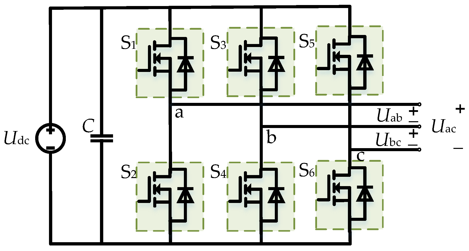
In high-power WPT systems, the specific arrangement of three-phase transmitter coils can be used to increase the output power of the inverter, equalize the magnetic field, and at the same time increase the system’s anti-offset characteristics [66,67,68]. The three-phase inverter adds one more bridge arm to the voltage-type H-bridge inverter to produce three outputs with a phase difference of 120°, which has the advantages of high efficiency, high power density, and easy realization of soft switching, as shown in Figure 15. At the same time, when the three-phase alternating current picked up by the secondary side rectifier, the pulsation frequency of the DC voltage is three times that of an ordinary single-phase inverter, so the capacity and volume of the DC filtering and energy storage device can be greatly reduced. Furthermore, four-phase or more phase inverters are also a promising way to further improve the output power and offset resistance of the system [69].
However, when the size of the three-phase output equivalent load or resonant frequency of the inverter is not the same, it is easy to lead to a three-phase current imbalance problem, which makes the output phase voltage distorted, increasing the total harmonic distortion (THD) and decreasing the working performance of the inverter. To solve the problem, Yu, S et al. adopted the current loop control based on PR controller, which can balance the three-phase currents better [70]. Xia, C et al. investigated a novel MOSFET turn-on-off hybrid symmetric phase-shift control strategy for three-phase inverters, which can realize the effective control of the output power of the WPT system under the premise of guaranteeing the soft-switching operation of the inverter [71].
Besides using multiphase inverters to enhance the power level of the system, connecting multiple inverters in parallel is also an effective method. The common multi-parallel inverter takes the voltage-type H-bridge inverter as the basic unit and provides the required power to the load by connecting the outputs in parallel; its basic topology is shown in Figure 16. This structure can be flexibly configured with the number of parallel inverters to meet the demands of different power levels of output and has the advantages of large capacity, modular replicability, and high redundancy [72,73].
However, circulating current problems can easily arise between the shunt inverters due to the differences in physical and control parameters, which may result in unequal power distribution between the inverters as well as difficulty in realizing soft switching. Mai, R. et al. proposed a circulating current elimination technique combining series-parallel resonant and phase regulation to reduce the circulating current for improving the efficiency and reliability of the system, but it requires complex control and detection sampling circuits [74]. Rahnamaee, H.R et al. proposed the method of adding coupled inductors at the output of each half-bridge inverter to keep the output current magnitude and phase of each inverter consistent, but the addition of coupled inductors also increases the size of the inverter and reduces the power density [75].
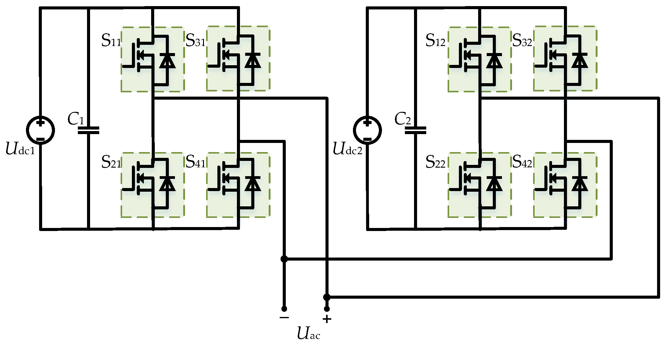
As for the multiphase inverter, it needs to solve the unbalance problem of each phase output current caused by the asymmetry of each phase load, while the multi-parallel inverter needs to face the circulating current problem due to the parameter differences among inverters. Multilevel inverters use low voltage capacity MOSFETs to generate high amplitude output voltages with the advantages of low MOSFET voltage stress and low du/dt. Meanwhile, compared with the above inverters, the output voltage waveform of the multilevel inverter is closer to a sinewave with lower THD, so it can reduce the high-frequency electromagnetic interference while increasing the output power of the system [76,77]. The cascaded H-bridge multilevel inverter is made by cascading the outputs of several full-bridge inverters; there is no capacitor voltage imbalance problem, the circuit is more reliable and can be modularized more easily, as shown in Figure 17. Rahnamaee, H. R. et al. proposed a bidirectional WPT system for electric vehicles based on a cascaded H-bridge multilevel inverter, which utilizes high-frequency low-voltage Si-MOSFETs to increase the system output power and operating frequency [78]. Li, Y. et al., on the other hand, proposed a harmonic elimination and power regulation method for five-level inverters, which improved the operating performance of the inverter [79]. However, the cascaded H-bridge multilevel inverter requires several isolated DC power supplies. In practical applications, it is not easy to obtain more than one isolated DC power supply, so its application area will be limited to a certain extent.
To solve this problem, Ge, X. et al. proposed a Single-Source Switched-Capacitor (S3C) multilevel inverter [80], as shown in Figure 18. The inverter requires only one DC input power supply and contains two half-bridges and several replicable I-type switch modules, which can generate higher voltage multilevel outputs and, thus, increases the system output power and lowers the THD of the inverter output voltage while guaranteeing that the voltage stresses of all the MOSFETs are not higher than the DC input voltage. It also allows for a stronger capacitor-voltage self-balancing capability as well as fewer MOSFETs and energy storage devices.
For high power applications of WPT systems, H-bridge inverters are the most common choice. With the increasing power level of WPT systems, multiphase inverters, multi-parallel inverters, and multilevel inverters have also come into being, and now as well as being able to reach power outputs up to the 100 kW level, a comparison of the performance of various types of H-bridge inverter circuits and their derived topologies is shown in Table 2.

4. Critical Techniques for High-Frequency Inverters

Currently, there has been some progress in the research of high-frequency inverters applied to WPT systems, which can operate at multi-MHz frequency at higher power levels.
In the area of high-frequency high-power inverter research, Drexel University in the United States explores the switching limit of the SiC full-bridge inverter at multi-kW power levels and firstly achieves a kilowatt high power level at a multi-MHz switching frequency with 4.39 kW at 3 MHz. This research was finally successfully applied to the CPT system [53]. The University of Tennessee validated the performance enhancement of GaN for high-frequency inverters in WPT systems by accurately modeling high-frequency transients in the junction capacitance of GaN devices with good heat dissipation design. A 6.6 kW power test at 3.125 MHz through a 100 mm air gap validates the concept of high- frequency WPT system for electric vehicles [81]. In terms of adaptation of the inverter to work with the WPT system, researchers at the University of Tokyo, Japan, applied a DC–DC converter to a WPT system and realized that the system always maintains the maximum transmission efficiency when the load varies [82]. Researchers at Chongqing University in China have also conducted a lot of research on the soft-switching technology and system control of high-frequency inverter circuits for WPT systems, and have achieved a lot of results [83,84].
Resonant power amplifiers, while having fewer numbers of MOSFETs, simpler topologies, smaller parasitic parameters, and simpler gate drive circuits, are favorable for high-frequency operation above MHz. However, since the voltage stress on the amplifier switches tends to be much higher than the input DC voltage, the H-bridge inverter topology should still be the main candidate when it comes to kW high-power applications. Figure 19 shows the circuit model of the H-bridge inverter containing parasitic parameters, where S1~S4 are the four switches, Ldc1~Ldc4 are the DC-side parasitic inductances, and LD1~LD4 and LS1~LS4 are the device lead and circuit alignment parasitic inductances. Cgd, Cgs, and Cds are the parasitic junction capacitances of the MOSFETs, and LD(int), LS(int), and RG(int) are the internal parasitic inductances and resistances, respectively. Vdrive is the voltage source of the drive circuit, and LG is the total parasitic inductance of the drive circuit. Rg(ext) is the externally added drive resistor [11].
Herein, the MOSFET input capacitance, Ciss, output capacitance, Coss, and reverse recovery capacitance, Crss, are expressed in Equation (2), which can be found in the device datasheet.
{ C iss = C gs + C gd C oss = C ds + C gd C rss = C gd
When the device operates at high frequency, the effects of parasitic parameters become insignificant. Typically, RG(int) and Cgs reduce the speed of switching, leading to additional power loss. Cds makes it difficult to realize ZVS, leading to switching losses and drain-source oscillations. Cgd and LS(int) cause coupling between the control side and the power side, which can cause disturbances to the driver circuit when dv/dt and di/dt are high.
Regarding this, researchers have proposed various methods to reduce the effect of parasitic parameters. In general, it can be divided into two main technical routes: reducing the impact of parasitic parameters on the inverter; reducing the value of parasitic parameters.
The study of the effect of parasitic parameters on the inverter includes the following aspects: for the drain-source oscillation caused by parasitic parameters, the most used method is to connect RC snubber circuits in parallel at both ends of the MOSFETs, which has been widely used in low-frequency inverters. However, in high-frequency operation, RC snubber circuits result in higher power loss, which is not beneficial to the efficient design of the system. Josifović, I. et al. proposed the use of ferrite beads to suppress oscillations and effectively reduce switching losses [85]. To solve the problem of interference of parasitic parameters to the driving circuit, the minimization design of common source inductance (LS) can reduce the coupling between the control side and the power side; thus, reducing the interference of the power loop to the driving circuit [86]. The bipolar driving strategy achieves a more reliable turn-off of the MOSFETs by applying a negative Vgs during the turn-off period, preventing the mis-conduction phenomenon due to the charging of Cgs. As for the overshoot in device voltage and current during switching transients of MOSFETs caused by high di/dt and dv/dt, Nayak, P. et al. proposed a quasi-zero voltage switching (QZV) control method to make the inverter work properly with proper layout parasitic inductance and load parasitic capacitance [87].
In order to reduce the values of parasitic parameters, from the perspective of PCB design, conformal mappings and electromagnetic full wave planar simulator have been applied to analyze the effect of PCB layout alignment on parasitic parameters and to provide guidance for PCB design that minimizes parasitic parameters [88]. From the perspective of device package, Ionescu, C. et al. analyzed the effect of package parasitic inductance on the device switching characteristics and established a GaN-HEMT simulation model to provide theoretical support for package optimization of switching devices [89].
When considering the selection of devices for high frequency inverters, there are two main factors to focus on: the device’s high-speed switching capability and whether it is easy to realize soft switching. High-speed switching capability is the shortest possible on/off transient, i.e., the short rise/fall time of the gate drive signal. During the switching transient, the drive power supply Vdrive charges and discharges the gate input capacitor Ciss to realize the control of MOSFET on–off, so the drive loop parameters LG, RG(ext), RG(int), and Ciss affect the switching speed. The switching speed is mainly determined by the RG(int) and Ciss of a MOSFET by minimizing the external parameters PCB layout optimization of LG and RG(ext) by the inverter. The charging of Ciss during the on-state transient is shown in Equation (3). Vgs is the transient gate-source voltage, and tr is the rise time during the transient on-state. The results show that RG(int) and the total gate charge Qg determine the conduction rate.
0 t r V d r i v V g s d t = Q g R G ( int )
During ZVS operation, the parasitic output capacitance Coss of the MOSFET that will be turned on needs to be fully discharged, and its body diode needs to quickly switch from the blocking state to the forward-biased state during the dead time and remain on throughout the on-state transient, clamping the drain-source voltage at 0 V. Therefore, small losses and fast recovery of the body diode are essential to create ZVS operating conditions, which can be expressed in terms of the reverse recovery charge of the MOSFET, Qrr. Qrr denotes the reverse recovery charge at a specific reverse blocking voltage, which consists of the losses stored in the body diode and the charge in the PN junction. Low Qrr helps to achieve high ZVS.

5. Potential Issues and Future Research Directions

5.1. Potential Issues

5.1.1. High Frequency Loss of Inductors

Inductors play an important role in inverters, especially in current-type inverters, and their size and loss greatly affect the size and efficiency of the whole converter. Air-core inductors tend to be bulkier compared to magnetic-core inductors of the same capacity, which is not beneficial to the miniaturization design of inverters and, thus, magnetic cores are usually used in power electronic circuits to reduce the size of inductors.
With the development of high frequency inverters, the volume and weight of inductors can be reduced, but the core loss and heat generation increase with the frequency, which will lead to the deterioration of inverter working conditions and lower efficiency. In the design of future inverters, the frequency characteristics of magnetic components should be fully considered, and the additional loss caused by high frequency should be reduced from the perspectives of magnetic material selection and inductor structure optimization.

5.1.2. Mutual Constraints on Operating Frequency and Power Level of Inverters

High-frequency characteristics require MOSFETs with high-speed switching capability, and the parasitic parameters of the package are expected to be smaller. However, the high-power characteristics require MOSFETs to have high withstand voltage and a high current capability, and these MOSFETs tend to have larger package parasitic parameters. Therefore, in the selection process of inverter MOSFETs, low parasitic parameters and large capacity are often contradictory to each other, and MOSFETs often need to make trade-offs between high-speed switching capability and high withstand voltage/current capability.
In addition, power amplifier circuits such as class-E are often able to achieve higher operating frequencies due to fewer switching devices and simpler driving, but this also leads to problems such as excessive MOSFET voltage stress and concentrated heat generation, which are not beneficial to the improvement of the power level. H-bridge inverters and the derived topologies are able to achieve tens or even hundreds of kilowatts of power level, but the complex circuit structure and driving method make it difficult for them to realize the application at higher frequencies. Therefore, there is also a trade-off between frequency and power in the selection of circuit topology.

5.2. Future Research Directions

5.2.1. Driving Technology

As the operating frequency of the MOSFET increases, the power loss of the hard drive circuit will increase rapidly. In the high-frequency case, the hard-drive mode not only has the problem of large loss but also needs to provide large current for the hard-drive circuit to improve the switching speed. In addition, the anti-interference ability of the hard-drive circuit is weak, which can easily cause the false conduction of the switch.
In order to solve the above problems and obtain better performance in high-frequency applications, resonant gate driver (RGD) circuits have gradually become a hot research topic in recent years [90,91]. The simplest resonant drive circuit transfers the energy stored in capacitor Cg by adding a resonant inductor to reduce the energy loss, and the switching speed can be increased. Two other common types of resonant drive circuits are the H-bridge structure and the half-bridge structure. Half-bridge circuits require two additional diodes compared to H-bridge circuits, but H-bridge circuits have difficulty controlling the MOSFETs accurately at the end of each resonance cycle due to the Miller effect. In this respect, the half-bridge circuit shows better performance because the additional diode blocks the reverse resonance current at the end of each resonance cycle and, thus, allows for simpler control.

5.2.2. High Frequency Rectifier

The voltage and current input to the rectifier under high-frequency operation will have a large phase difference, and the simple equivalence into AC resistance will lead to inaccurate analysis [92]. An equivalent model of the full-bridge rectifier circuit considering the diode parasitic capacitance should be established, the operating modes of the rectifier bridge should be analyzed in the time domain, and the impedance characteristics of the full-bridge rectifier should be investigated.
In addition, for the field of High Frequency Rectifiers, class-E rectifiers are one of the most promising High Frequency Rectifier candidates due to their resonant structure [93,94,95]. Zero-voltage switching (ZVS) or zero-current switching (ZCS) can be realized through the rational design of resonant structure, which can effectively reduce the switching loss. Class-E rectifiers were first proposed and applied to high-frequency DC–DC converters in 1988, followed by a series of rectifiers for high-frequency conditions. They use naturally occurring component parasitic parameters to control the switching of diodes and, thus, minimizes parasitic ringing and improves rectifier efficiency by reducing harmonic currents. Later, the topology of class-E rectifiers was further developed, resulting in, for example, current-driven, voltage-driven, half-wave-driven, full-wave-driven, and active types.

5.2.3. Wide-Band Semiconductor Applications

Under high-frequency conditions, in addition to the resonant topology with good soft-switching characteristics, semiconductor devices with good high-frequency characteristics are also required to further reduce the system losses and improve the system efficiency. With the maturity of new material technology development, such as SiC and GaN material MOSFETs and high-frequency low-loss magnetic components, the efficiency of high-frequency power converters can be further improved [96].
GaN has a higher energy gap, electron mobility, and rate compared to SiC, making it more suitable for high-frequency applications. However, due to the small package, high-power GaN inverters usually require well-designed cooling systems. In addition, the high sensitivity of GaN MOSFETs to gate noise raises reliability issues for high power applications—factors that still need to be addressed using SiC MOSFETs.

6. Conclusions

This paper analyzes the potential of high-frequency inverters in WPT systems and establishes a performance evaluation system for inverters used in WPT systems. A comprehensive review of the two main topologies of high-frequency inverters (resonant power amplifier inverters based on the H-bridge inverter) applied to WPT systems is presented, and the advantages, disadvantages, and application scenarios of the different inverter topologies are fully analyzed, which provides a reference for the selection of inverters for WPT systems. Overall, resonant power amplifiers have better high-frequency characteristics, and inverters based on the H-bridge inverter are capable of achieving larger power levels. Parasitic parameters are the main constraints of high-frequency inverters, and this paper gives a specific method for switching device selection based on the analysis of the current status of parasitic parameter research. Finally, the potential issues and future research directions of high-frequency inverters for WPT systems are analyzed.

Author Contributions

Conceptualization, Y.L. and L.P.; methodology, L.P.; software, Y.L.; validation, Y.L.; formal analysis, S.Y.; investigation, L.P.; resources, S.Y.; data curation, J.Z.; writing—original draft preparation, Y.L.; writing—review and editing, S.Y. and L.P.; visualization, J.Z.; supervision, S.C. and C.Z.; project administration, J.Z.; funding acquisition, Y.L. All authors have read and agreed to the published version of the manuscript.

Funding

This work was supported by the National Natural Science Foundation of China under Project 52107002; Civil Space Technology Advance Research Program of China (D030303); and Postdoctoral Fellowship Program of CPSF under Grant Number GZC20233438.

Data Availability Statement

The data supporting the findings of this study are available by reasonable request to [email protected].

Conflicts of Interest

All co-authors have seen and agree with the contents of the manuscript and there is no financial interest to report. We certify that the submission is original work and is not under review at any other publication.

References

  1. Zhang, Z.; Pang, H.; Georgiadis, A.; Cecati, C. Wireless Power Transfer—An Overview. IEEE Trans. Ind. Electron. 2019, 66, 1044–1058. [Google Scholar] [CrossRef]
  2. Zhang, J.; Yao, S.; Pan, L.; Liu, Y.; Zhu, C. A Review of Capacitive Power Transfer Technology for Electric Vehicle Applications. Electronics 2023, 12, 3534. [Google Scholar] [CrossRef]
  3. Sun, M.; Dai, X.; Li, Y.; Su, Y. Research Status of Bidirectional Wireless Power Transfer Technology. In Proceedings of the 8th World Congress on Civil, Structural, and Environmental Engineering, Lisbon, Portugal, 29–31 March 2023; pp. 1–19. [Google Scholar]
  4. Williams, K.J.; Wiseman, K.; Deilami, S.; Town, G.; Taghizadeh, F. A Review of Power Transfer Systems for Light Rail Vehicles: The Case for Capacitive Wireless Power Transfer. Energies 2023, 16, 5750. [Google Scholar] [CrossRef]
  5. Yu, Z.; Xiao, W.; Zhang, B.; Qiu, D. Development Status of Electric-Field Coupled Wireless Power Transmission Technology. Trans. China Electrotech. Soc. 2022, 37, 1051–1069. [Google Scholar]
  6. Zhang, J.; Yao, S.; Wang, S.; Pan, L.; Liu, Y.; Zhu, C. Vertical Self-Coupling Plates Design for Capacitive Power Transfer System. In Proceedings of the International Conference on Wireless Power Transfer, ICWPT 2023, Weihai, China, 13–15 October 2023; Springer: Berlin/Heidelberg, Germany, 2024; Volume 1158 LNEE, pp. 136–144. [Google Scholar]
  7. Wang, D.; Zhang, J.; Zhu, C.; Bie, Z.; Cui, S. Review of Progress in the Study of Marine Environment Effects on Underwater Wireless Power Transfer Systems. Trans. China Electrotech. Soc. 2024, 1–22. [Google Scholar]
  8. Cai, J.; Wu, X.; Sun, P.; Sun, J.; Zhang, X. Research progress of magnetic coupling wireless power transmission technology and its high power realization method. J. Nav. Univ. Eng. 2021, 33, 19–27. [Google Scholar]
  9. Xue, M.; Yang, Q.; Zhang, P.; Guo, J.; Li, Y.; Zhang, X. Application Status and Key Issues of Wireless Power Transmission Technology. Trans. China Electrotech. Soc. 2021, 36, 1547–1568. [Google Scholar]
  10. Xingming, F.; Linlin, G.; Xiaoyong, M.; Qian, Z.; Erju, J. Overview of Research Status and Application of Wireless Power Transmission Technology. Trans. China Electrotech. Soc. 2019, 34, 1353–1380. [Google Scholar]
  11. Wang, Y.; Wang, K.; Li, K.; Yang, Y.; Hui, S.Y.R. Multi-MHz Inductive and Capacitive Power Transfer Systems with PCB-Based Self-Resonators. IEEE Trans. Power Electron. 2024, 39, 14077–14090. [Google Scholar] [CrossRef]
  12. Wang, Y.; Yang, Y.A. Comparative Review on the Development of High-Frequency and High-Power Capacitive Power Transfer Technology. In Proceedings of the 2024 10th International Conference on Power Electronics Systems and Applications (PESA), Hong Kong, 5–7 June 2024; pp. 1–9. [Google Scholar]
  13. Wang, Y.; Lucia, O.; Zhang, Z.; Guan, Y.; Xu, D. Review of Very High Frequency Power Converters and Related Technologies. IET Power Electron. 2020, 13, 1711–1721. [Google Scholar] [CrossRef]
  14. Kurs, A.; Karalis, A.; Moffatt, R.; Joannopoulos, J.D.; Fisher, P.; Soljacic, M. Wireless Power Transfer via Strongly Coupled Magnetic Resonances. Science 2007, 317, 83–86. [Google Scholar] [CrossRef] [PubMed]
  15. Rooij, M.A. The ZVS Voltage-Mode Class-D Amplifier, an eGaN® FET-Enabled Topology for Highly Resonant Wireless Energy Transfer. In Proceedings of the 2015 IEEE Applied Power Electronics Conference and Exposition (APEC), Charlotte, NC, USA, 15–19 March 2015; pp. 1608–1613. [Google Scholar]
  16. Phan, T.; Zulauf, G.; Fan, J.A.; Rivas-Davila, J.M. 1 kW, Multi-MHz Wireless Charging for Electric Transportation. In Proceedings of the 2020 IEEE 21st Workshop on Control and Modeling for Power Electronics (COMPEL), Aalborg, Denmark, 9–12 November 2020; pp. 1–7. [Google Scholar]
  17. Li, H.; Wang, K.; Huang, L.; Chen, W.; Yang, X. Dynamic Modeling Based on Coupled Modes for Wireless Power Transfer Systems. IEEE Trans. Power Electron. 2015, 30, 6245–6253. [Google Scholar] [CrossRef]
  18. Li, H.; Liu, Y.; Ying, Y.; Fu, M. Circular Capacitive Coupler for Stable Output Under Horizontal Misalignment. In Proceedings of the 2022 IEEE 31st International Symposium on Industrial Electronics (ISIE), Anchorage, AK, USA, 1 June 2022; pp. 768–773. [Google Scholar]
  19. Li, H.; Liu, Y.; Fu, M. Circular Capacitive Coupler With Multilayer Interleaving for Stable Output. IEEE Trans. Microw. Theory Tech. 2023, 71, 719–726. [Google Scholar] [CrossRef]
  20. Chu, S.Y.; Cui, X.; Zan, X.; Avestruz, A.-T. Transfer-Power Measurement Using a Non-Contact Method for Fair and Accurate Metering of Wireless Power Transfer in Electric Vehicles. IEEE Trans. Power Electron. 2022, 37, 1244–1271. [Google Scholar] [CrossRef]
  21. Wang, Y.; Liu, W.; Huangfu, Y. A Primary-Sided CLC Compensated Wireless Power Transfer System Based on the Class D Amplifier. In Proceedings of the IECON 2018—44th Annual Conference of the IEEE Industrial Electronics Society, Washington, DC, USA, 21–23 October 2018; pp. 943–947. [Google Scholar]
  22. Ge, X.; Cheng, L.; Ki, W.-H. A DCM ZVS Class-D Power Amplifier for Wireless Power Transfer Applications. In Proceedings of the 2019 IEEE Asian Solid-State Circuits Conference (A-SSCC), Macau, Macao, 4–6 November 2019; pp. 43–44. [Google Scholar]
  23. Shao, L.; Li, Q.; Tan, C.; Yao, K.; Song, J. A Study of Magnetic Resonance Wireless Power Transfer System Based on Half Bridge Inverter. In Proceedings of the 2016 IEEE Vehicle Power and Propulsion Conference (VPPC), Hangzhou, China, 17–20 October 2016; pp. 1–5. [Google Scholar]
  24. Mishima, T.; Morita, E. High-Frequency Bridgeless Rectifier Based ZVS Multiresonant Converter for Inductive Power Transfer Featuring High-Voltage GaN-HFET. IEEE Trans. Ind. Electron. 2017, 64, 9155–9164. [Google Scholar] [CrossRef]
  25. Choi, S.-J.; Choi, H.-S. Capacitive Wireless Power Transfer System with Double Matching Transformers for Reduced Stress and Extended ZVS Range. In Proceedings of the 2015 IEEE International Telecommunications Energy Conference (INTELEC), Osaka, Japan, 18–22 October 2015; pp. 1–6. [Google Scholar]
  26. Piedrahita-Echavarría, E.Y.; Alvarez-Duque, M.; Escobar-Mejía, A.; Gil-González, W. Design and Control of a Series-Parallel Compensation Topology for Wireless Power Transfer Applications. In Proceedings of the 2023 IEEE 6th Colombian Conference on Automatic Control (CCAC), Popayan, Columbia, 17–20 October 2023; pp. 1–6. [Google Scholar]
  27. Choi, U.-G.; Yang, J.-R. A 120 W Class-E Power Module with an Adaptive Power Combiner for a 6.78 MHz Wireless Power Transfer System. Energies 2018, 11, 2083. [Google Scholar] [CrossRef]
  28. Weng, Y.-C.; Wu, C.-C.; Chang, E.L.; Chieng, W.-H. Minimum Power Input Control for Class-E Amplifier Using Depletion-Mode Gallium Nitride High Electron Mobility Transistor. Energies 2021, 14, 2302. [Google Scholar] [CrossRef]
  29. Wen, F.; Li, R. Parameter Analysis and Optimization of Class-E Power Amplifier Used in Wireless Power Transfer System. Energies 2019, 12, 3240. [Google Scholar] [CrossRef]
  30. Xiao, W.; Shen, R.; Zhang, B.; Qiu, D.; Chen, Y.; Li, T. Effects of Foreign Metal Object on Soft-Switching Conditions of Class-E Inverter in WPT. Energies 2018, 11, 1926. [Google Scholar] [CrossRef]
  31. Narayanamoorthi, R.; Juliet, V.A.; Chokkalingam, B.; Padmanaban, S.; Leonowicz, Z.M. Class E Power Amplifier Design and Optimization for the Capacitive Coupled Wireless Power Transfer System in Biomedical Implants. Energies 2017, 10, 1409. [Google Scholar] [CrossRef]
  32. Li, B.; Ngo, K. Analysis and Design of an Isolated Current Source Class-E Inverter With Significant Harmonics. IEEE Trans. Power Electron. 2024, 39, 14877–14887. [Google Scholar] [CrossRef]
  33. Aditya, K.; Pradhan, S.; Raj, A. Class-E Power Amplifier Design for Wireless Power Transfer. In Proceedings of the 2024 IEEE 3rd International Conference on Electrical Power and Energy Systems (ICEPES), Bhopal, India, 21–22 June 2024; pp. 1–5. [Google Scholar]
  34. Lai, C.-M.; Lin, D.-T.; Liu, H.-E.; Mishima, T.; Tse, C.K. A Single-Stage DC Motor Driver Based on Class-E Resonant Wireless Power Transfer Technique. In Proceedings of the 2023 IEEE Transportation Electrification Conference and Expo, Asia-Pacific (ITEC Asia-Pacific), Chiang Mai, Thailand, 28 November–1 December 2023; pp. 1–7. [Google Scholar]
  35. Xu, J.; Tong, Z.; Rivas-Davila, J. 1 kW MHz Wideband Class E Power Amplifier. In Proceedings of the 2021 IEEE 22nd Workshop on Control and Modelling of Power Electronics (COMPEL), Cartagena, Colombia, 2–5 November 2021; pp. 1–6. [Google Scholar]
  36. Sample, A.P.; Waters, B.H.; Wisdom, S.T.; Smith, J.R. Enabling Seamless Wireless Power Delivery in Dynamic Environments. Proc. IEEE 2013, 101, 1343–1358. [Google Scholar] [CrossRef]
  37. Song, J.; Liu, M.; Ma, C. Analysis and Design of a High-Efficiency 6.78-MHz Wireless Power Transfer System With Scalable Number of Receivers. IEEE Trans. Ind. Electron. 2020, 67, 8281–8291. [Google Scholar] [CrossRef]
  38. Liu, M.; Zhao, C.; Song, J.; Ma, C. Battery Charging Profile-Based Parameter Design of a 6.78-MHz Class E^2 Wireless Charging System. IEEE Trans. Ind. Electron. 2017, 64, 6169–6178. [Google Scholar] [CrossRef]
  39. Nagashima, T.; Wei, X.; Suetsugu, T.; Sekiya, H. Inductively Coupled Wireless Power Transfer with Class-DE Power Amplifier. In Proceedings of the 2012 IEEE Asia Pacific Conference on Circuits and Systems, Kaohsiung, Taiwan, 2–5 December 2012; pp. 73–76. [Google Scholar]
  40. Nikiforidis, I.; Kwan, C.H.; Yates, D.C.; Bampouras, K.; Gawith, J.; Pucci, N.; Mitcheson, P.D. A 3 kW 3.39 MHz DC/DC Inductive Power Transfer System with Power Combining Converters. In Proceedings of the 2023 IEEE Wireless Power Technology Conference and Expo (WPTCE), San Diego, CA, USA, 4–8 June 2023; pp. 1–6. [Google Scholar]
  41. Aviles, J.P.O.; Tofoli, F.L.; Ribeiro, E.R. Novel Control Approach for Resonant Class-DE Inverters Applied in Wireless Power Transfer Systems. Energies 2023, 16, 7238. [Google Scholar] [CrossRef]
  42. Raab, F.H. Class-F Power Amplifiers with Maximally Flat Waveforms. IEEE Trans. Microw. Theory Tech. 1997, 45, 2007–2012. [Google Scholar] [CrossRef]
  43. Huang, X.; Lin, Y.; Dou, Y.; Lin, S.; Huang, J. Load-Independent Push–Pull Class-Φ2 Inverter With Single Compact Three-Winding Inductor. IEEE Trans. Power Electron. 2023, 38, 11916–11927. [Google Scholar] [CrossRef]
  44. Aldhaher, S.; Yates, D.C.; Mitcheson, P.D. Design and Development of a Class EF2 Inverter and Rectifier for Multimegahertz Wireless Power Transfer Systems. IEEE Trans. Power Electron. 2016, 31, 8138–8150. [Google Scholar] [CrossRef]
  45. Choi, J.; Tsukiyama, D.; Rivas, J. Evaluation of a 900 V SiC MOSFET in a 13.56 MHz 2 kW Resonant Inverter for Wireless Power Transfer. In Proceedings of the 2016 IEEE 17th Workshop on Control and Modeling for Power Electronics (COMPEL), Trondheim, Norway, 27–30 June 2016; pp. 1–6. [Google Scholar]
  46. Choi, J.; Tsukiyama, D.; Rivas, J. Comparison of SiC and eGaN Devices in a 6.78 MHz 2.2 kW Resonant Inverter for Wireless Power Transfer. In Proceedings of the 2016 IEEE Energy Conversion Congress and Exposition (ECCE), Milwaukee, WI, USA, 18–22 September 2016; pp. 1–6. [Google Scholar]
  47. Zhou, X.; Wang, J.; Yang, L. A Light-Load Efficiency Improvement Technique for an Inductive Power Transfer System through a Reconfigurable Circuit. Energies 2024, 17, 3024. [Google Scholar] [CrossRef]
  48. Kumar, A.; Bertoluzzo, M.; Jha, R.K.; Sagar, A. Analysis of Losses in Two Different Control Approaches for S-S Wireless Power Transfer Systems for Electric Vehicle. Energies 2023, 16, 1795. [Google Scholar] [CrossRef]
  49. Lee, S.-H.; Yi, K.-P.; Kim, M.-Y. 6.78-MHz, 50-W Wireless Power Supply Over a 60-Cm Distance Using a GaN-Based Full-Bridge Inverter. Energies 2019, 12, 371. [Google Scholar] [CrossRef]
  50. Lu, F.; Zhang, H.; Mi, C. A Review on the Recent Development of Capacitive Wireless Power Transfer Technology. Energies 2017, 10, 1752. [Google Scholar] [CrossRef]
  51. Sinha, S.; Regensburger, B.; Doubleday, K.; Kumar, A.; Pervaiz, S.; Afridi, K.K. High-Power-Transfer-Density Capacitive Wireless Power Transfer System for Electric Vehicle Charging. In Proceedings of the 2017 IEEE Energy Conversion Congress and Exposition (ECCE), Cincinnati, OH, USA, 1–5 October 2017; pp. 967–974. [Google Scholar]
  52. Lu, F.; Zhang, H.; Hofmann, H.; Mi, C. A CLLC-Compensated High Power and Large Air-Gap Capacitive Power Transfer System for Electric Vehicle Charging Applications. In Proceedings of the 2016 IEEE Applied Power Electronics Conference and Exposition (APEC), Long Beach, CA, USA, 20–24 March 2016; pp. 1721–1725. [Google Scholar]
  53. Wang, Y.; Kheirollahi, R.; Lu, F.; Zhang, H. Exploring Switching Limit of SiC Inverter for Multi-kW Multi-MHz Wireless Power Transfer System. In Proceedings of the 2023 IEEE Applied Power Electronics Conference and Exposition (APEC), Orlando, FL, USA, 19–23 March 2023; pp. 2952–2957. [Google Scholar]
  54. Chang, E.-C. Improving Performance for Full-Bridge Inverter of Wind Energy Conversion System Using a Fast and Efficient Control Technique. Energies 2018, 11, 262. [Google Scholar] [CrossRef]
  55. Wang, Y.; Zhang, H.; Lu, F. Current-Fed Capacitive Power Transfer With Parallel–Series Compensation for Voltage Step-Down. IEEE J. Emerg. Sel. Top. Ind. Electron. 2022, 3, 454–464. [Google Scholar] [CrossRef]
  56. Samanta, S.; Rathore, A.K. A New Current-Fed CLC Transmitter and LC Receiver Topology for Inductive Wireless Power Transfer Application: Analysis, Design, and Experimental Results. IEEE Trans. Transp. Electrif. 2015, 1, 357–368. [Google Scholar] [CrossRef]
  57. Samanta, S.; Rathore, A.K.; Sahoo, S.K. Concept Study and Feasibility Analysis of Current-Fed Power Electronics for Wireless Power Transfer System. In Proceedings of the 2016 IEEE International Conference on Power Electronics, Drives and Energy Systems (PEDES), Trivandrum, India, 14–17 December 2016; pp. 1–6. [Google Scholar]
  58. Fan, F.; Chen, Q.; Wang, J.; Chen, W. Accurate Calculation Method of Rectifier Load and Time-Domain Analysis in PS/S Current-Fed WPT System. In Proceedings of the 2022 IEEE 5th International Electrical and Energy Conference (CIEEC), Nangjing, China, 27–29 May 2022; pp. 466–471. [Google Scholar]
  59. Waite, M.; Zane, R.; Wang, H. A New Current-Fed Inductive Wireless Charging Transmitter for Large-Scale EV In-Motion Wireless Charging Infrastructure. In Proceedings of the 2024 IEEE Wireless Power Technology Conference and Expo (WPTCE), Kyoto, Japan, 8–11 May 2024; pp. 193–198. [Google Scholar]
  60. Li, Y.; Duan, Q.; Li, W. A Short-Current Control Method for Constant Frequency Current-Fed Wireless Power Transfer Systems. Energies 2017, 10, 585. [Google Scholar] [CrossRef]
  61. Duan, Q.; Li, Y.; Dai, X.; Zou, T. A Novel High Controllable Voltage Gain Push-Pull Topology for Wireless Power Transfer System. Energies 2017, 10, 474. [Google Scholar] [CrossRef]
  62. Yu, A.; Zeng, X.; Xiong, D.; Tian, M.; Li, J. An Improved Autonomous Current-Fed Push-Pull Parallel-Resonant Inverter for Inductive Power Transfer System. Energies 2018, 11, 2653. [Google Scholar] [CrossRef]
  63. Mishima, T.; Liu, S.; Taguchi, R.; Lai, C.-M. MHz-Driven Snubberless Soft-Switching Current-Fed Multiresonant DC–DC Converter. IEEE Trans. Power Electron. 2024, 39, 8404–8416. [Google Scholar] [CrossRef]
  64. Hu, A.P.; Liu, C.; Li, H.L. A Novel Contactless Battery Charging System for Soccer Playing Robot. In Proceedings of the 2008 15th International Conference on Mechatronics and Machine Vision in Practice, Auckland, New Zealand, 2–4 December 2008; pp. 646–650. [Google Scholar]
  65. Namadmalan, A. Bidirectional Current-Fed Resonant Inverter for Contactless Energy Transfer Systems. IEEE Trans. Ind. Electron. 2015, 62, 238–245. [Google Scholar] [CrossRef]
  66. Mai, R.; Li, H.; Liu, Y.; Zhou, K.; Fu, L.; He, Z. A Three-Phase Dynamic Wireless Charging System with Constant Output Voltage. Energies 2018, 11, 45. [Google Scholar] [CrossRef]
  67. Colussi, J.; La Ganga, A.; Re, R.; Guglielmi, P.; Armando, E. 100 kW Three-Phase Wireless Charger for EV: Experimental Validation Adopting Opposition Method. Energies 2021, 14, 2113. [Google Scholar] [CrossRef]
  68. Colussi, J.; Re, R.; Guglielmi, P. Modelling and Design of a Coils Structure for 100 kW Three-Phase Inductive Power Transfer System. Energies 2022, 15, 5079. [Google Scholar] [CrossRef]
  69. Huang, Z.; Xie, R.; Pan, W.; Shen, Z.; Zhuang, Y.; Zhang, Y. Integrated Four-LCC-Parallel Circuit for Wireless Power Transfer of Electric Vehicles with Vector Synthesis Strategy. In Proceedings of the 2024 IEEE 19th Conference on Industrial Electronics and Applications (ICIEA), Kristiansand, Norway, 5–8 August 2024; pp. 1–6. [Google Scholar]
  70. Yu, Y.; Nian, C.; Xie, G.; Liu, Z.; Jia, N.; Xia, C.; Wu, X. Current control strategy of three-phase series resonant inverter under unbalanced load. Trans. China Electrotech. Soc. 2014, 29, 49–53. [Google Scholar]
  71. Xia, C.; Zhuang, Y.; Jia, N.; Wu, X. Research on mixed symmetric control scheme for three-phase series resonance inverter system. J. Sichuan Univ. Eng. Sci. Ed. 2013, 45, 143–148. [Google Scholar]
  72. Hao, H.; Covic, G.A.; Boys, J.T. A Parallel Topology for Inductive Power Transfer Power Supplies. IEEE Trans. Power Electron. 2014, 29, 1140–1151. [Google Scholar] [CrossRef]
  73. Deng, Q.; Sun, P.; Hu, W.; Czarkowski, D.; Kazimierczuk, M.K.; Zhou, H. Modular Parallel Multi-Inverter System for High-Power Inductive Power Transfer. IEEE Trans. Power Electron. 2019, 34, 9422–9434. [Google Scholar] [CrossRef]
  74. Mai, R.; Lu, L.; Li, Y.; Lin, T.; He, Z. Circulating Current Reduction Strategy for Parallel-Connected Inverters Based IPT Systems. Energies 2017, 10, 261. [Google Scholar] [CrossRef]
  75. Bojarski, M.; Asa, E.; Czarkowski, D. Three-Phase Resonant Inverter for Wireless Power Transfer. In Proceedings of the 2015 IEEE Wireless Power Transfer Conference (WPTC), Boulder, CO, USA, 13–15 May 2015; pp. 1–4. [Google Scholar]
  76. Afonso, J.L.; Lisboa Cardoso, L.A.; Pedrosa, D.; Sousa, T.J.C.; Machado, L.; Tanta, M.; Monteiro, V. A Review on Power Electronics Technologies for Electric Mobility. Energies 2020, 13, 6343. [Google Scholar] [CrossRef]
  77. Shevchenko, V.; Pakhaliuk, B.; Husev, O.; Veligorskyi, O.; Stepins, D.; Strzelecki, R. Feasibility Study GaN Transistors Application in the Novel Split-Coils Inductive Power Transfer System with T-Type Inverter. Energies 2020, 13, 4535. [Google Scholar] [CrossRef]
  78. Rahnamaee, H.R.; Thrimawithana, D.J.; Madawala, U.K. MOSFET Based Multilevel Converter for IPT Systems. In Proceedings of the 2014 IEEE International Conference on Industrial Technology (ICIT), Busan, Republic of Korea, 26 February–1 March 2014; pp. 295–300. [Google Scholar]
  79. Li, Y.; Mai, R.; Lu, L.; He, Z. A harmonic elimination and power regulation approach of a cascaded multilevel technology in IPT systems. Proc. CSEE 2015, 35, 5278–5285. [Google Scholar]
  80. Ge, X.-J.; Sun, Y.; Wang, Z.-H.; Tang, C.-S. A Single-Source Switched-Capacitor Multilevel Inverter for Magnetic Coupling Wireless Power Transfer Systems. Electr. Eng. 2019, 101, 1083–1094. [Google Scholar] [CrossRef]
  81. Qin, R.; Li, J.; Costinett, D. A 6.6-kW High-Frequency Wireless Power Transfer System for Electric Vehicle Charging Using Multilayer Nonuniform Self-Resonant Coil at MHz. IEEE Trans. Power Electron. 2022, 37, 4842–4856. [Google Scholar] [CrossRef]
  82. Jiang, Y.; Wang, L.; Wang, Y.; Liu, J.; Li, X.; Ning, G. Analysis, Design, and Implementation of Accurate ZVS Angle Control for EV Battery Charging in Wireless High-Power Transfer. IEEE Trans. Ind. Electron. 2019, 66, 4075–4085. [Google Scholar] [CrossRef]
  83. Sun, M.; Dai, X.; Su, Y.; Li, Y.; Zhao, S. Frequency and Phase Synchronous Control Method Without Communication of the BCPT System. IEEE Trans. Power Electron. 2024, 39, 4792–4804. [Google Scholar] [CrossRef]
  84. Dai, X.; Sun, M.; Deng, P.; Wang, R.; Su, Y. Asymmetric Bidirectional Capacitive Power Transfer Method With Push–Pull Full-Bridge Hybrid Topology. IEEE Trans. Power Electron. 2022, 37, 13902–13913. [Google Scholar] [CrossRef]
  85. Josifović, I.; Popović-Gerber, J.; Ferreira, J.A. Improving SiC JFET Switching Behavior Under Influence of Circuit Parasitics. IEEE Trans. Power Electron. 2012, 27, 3843–3854. [Google Scholar] [CrossRef]
  86. Niu, Y.-C.; Huang, Y.-T.; Chen, C.-L.; Chen, Y.-M. Design Considerations of the Gate Drive Circuit for GaN HEMT Devices. In Proceedings of the 2018 Asian Conference on Energy, Power and Transportation Electrification (ACEPT), Singapore, 30 October–2 November 2018; pp. 1–6. [Google Scholar]
  87. Nayak, P.; Hatua, K. Parasitic Inductance and Capacitance-Assisted Active Gate Driving Technique to Minimize Switching Loss of SiC MOSFET. IEEE Trans. Ind. Electron. 2017, 64, 8288–8298. [Google Scholar] [CrossRef]
  88. Ionescu, C. Analysis of PCB Parasitic Influences in Uninterruptible Power Supplies. In Proceedings of the 24th International Spring Seminar on Electronics Technology. Concurrent Engineering in Electronic Packaging ISSE 2001 (Cat. No.01EX492), Calimanesti-Caciulata, Romania, 5–9 May 2001; pp. 83–87. [Google Scholar]
  89. Liu, Z.; Huang, X.; Lee, F.C.; Li, Q. Package Parasitic Inductance Extraction and Simulation Model Development for the High-Voltage Cascode GaN HEMT. IEEE Trans. Power Electron. 2014, 29, 1977–1985. [Google Scholar] [CrossRef]
  90. Huang, Y.; Zhang, J.; Wang, N. A Resonant Auxiliary Drive Circuit for SiC MOSFET to Suppress Crosstalk. Trans. China Electrotech. Soc. 2022, 37, 3004–3015. [Google Scholar]
  91. Zhao, Q.; Cui, S.; Yuan, J.; Wang, D. Resonant Drive Technology and Reverse Conduction Characteristics of Low Voltage GaN Devices. Trans. China Electrotech. Soc. 2019, 34, 133–140. [Google Scholar]
  92. Wu, Y.; Chen, Q.; Ren, X.; Zhang, Z. Efficiency Optimization Based Parameter Design Method for the Capacitive Power Transfer System. IEEE Trans. Power Electron. 2021, 36, 8774–8785. [Google Scholar] [CrossRef]
  93. Song, J.; Liu, M.; Ma, C. Class E Active Rectifier with Controlled Output Voltage for MHz Wireless Power Transfer. In Proceedings of the IECON 2020 The 46th Annual Conference of the IEEE Industrial Electronics Society, Singapore, 18–21 October 2020; pp. 4561–4565. [Google Scholar]
  94. Fu, X.; Liu, M.; Tang, Z.; Ma, C. Design Procedure of a Class E2 DC-DC Converter for Megahertz Wireless Power Transfer Based on a Compact Class E Current-Driven Rectifier. In Proceedings of the 2017 IEEE 26th International Symposium on Industrial Electronics (ISIE), Edinburgh, UK, 19–21 June 2017; pp. 694–699. [Google Scholar]
  95. Liu, M.; Fu, M.; Ma, C. A Compact Class E Rectifier for Megahertz Wireless Power Transfer. In Proceedings of the 2015 IEEE PELS Workshop on Emerging Technologies: Wireless Power (2015 WoW), Daejeon, Republic of Korea, 5–6 June 2015; pp. 1–5. [Google Scholar]
  96. Chevinly, J.; Rad, S.S.; Nadi, E.; Proca, B.; Wolgemuth, J.; Calabro, A.; Zhang, H.; Lu, F. Gallium Nitride (GaN) Based High-Power Multilevel H-Bridge Inverter for Wireless Power Transfer of Electric Vehicles. In Proceedings of the 2024 IEEE Transportation Electrification Conference and Expo (ITEC), Chicago, IL, USA, 19–21 June 2024; pp. 1–5. [Google Scholar]
Figure 1. Structure of WPT system.
Energies 17 05153 g001
Figure 2. Classification of inverters in the WPT system.
Energies 17 05153 g002
Figure 3. The criteria for evaluating the inverters.
Energies 17 05153 g003
Figure 4. Class-D power amplifier.
Energies 17 05153 g004
Figure 5. Half-bridge inverter.
Energies 17 05153 g005
Figure 6. Class-E power amplifier.
Energies 17 05153 g006
Figure 7. Double Class-E power amplifier.
Energies 17 05153 g007
Figure 8. WPT system with π-type impedance matching network.
Energies 17 05153 g008
Figure 9. WPT system with L-type impedance matching network.
Energies 17 05153 g009
Figure 10. Class-DE power amplifier.
Energies 17 05153 g010
Figure 11. Class-Φ2 power amplifier.
Energies 17 05153 g011
Figure 12. H-bridge inverter: (a) voltage-type inverter; (b) current-type inverter.
Energies 17 05153 g012
Figure 13. Push–pull inverter.
Energies 17 05153 g013
Figure 14. Self-oscillating push-pull inverter.
Energies 17 05153 g014
Figure 15. Three-phase inverter.
Energies 17 05153 g015
Figure 16. Double parallel inverter.
Energies 17 05153 g016
Figure 17. Cascaded H-bridge multilevel inverter.
Energies 17 05153 g017
Figure 18. S3C multilevel inverter.
Energies 17 05153 g018
Figure 19. Equivalent circuit of H-bridge inverter with parasitic parameters.
Energies 17 05153 g019
Table 1. Comparison of the performance of various types of power amplifiers.
LiteraturesPower AmplifiersAdvantagesDisadvantagesPower Level
[15,16,17,18,19,20,21,22]Class-DSimple structure and small sizeDC component present in output, complex high side drivelow
[23,24,25,26]Half-bridgeNo DC component, more flexible compensationLow power density; capacitor voltage equalization issuesmedium
[27,28,29,30,31,32,33,34,35,37,38]Class-EHigh efficiency, suitable for high frequencyHigh MOSFET voltage stress, sensitive system parameterslow
[5]Double Class-EHigh efficiency, higher powerHigh system complexity due to increased switching devicesmedium
[39,40,41]Class-DELow MOSFET voltage stress, high efficiencyDifficult to controlmedium
[43,44,45,46]Class-EFnLess output harmonic content, more efficient systemAdding extra devices increases the cost and volumelow
Table 2. Performance comparison of various types of inverters based on H-bridge.
LiteraturesInvertersAdvantagesDisadvantagesPower Level
[47,48,49,50,51,52,53,54]H-bridge inverter (voltage-type)Better load adaptability, high power densityDead time needs to be set, body diode reverse recovery needs to be consideredhigh
[55,56,57,58,59,60]H-bridge inverter (current-type)short-circuit resistance, capable of voltage pumping upLow power density, poor load adaptabilityhigh
[61,62,63,64,65]Push-pull inverterSelf-excited oscillation drive, no need for external drive circuitryLow power density, sensitive to system parametershigh
[66,67,68,69,70,71]Three-phase inverterIncreases output power, equalizes magnetic field, and increases the offset resistanceOutput current imbalance in each phase due to load asymmetryultra-high
[72,73,74,75]multi-parallel inverterFlexible configuration of output power, easy redundancy designCirculation due to parameter differences between invertersultra-high
[76,77,78,79,80]multilevel inverterIncrease power while reducing EMIComplexity of controlultra-high
Disclaimer/Publisher’s Note: The statements, opinions and data contained in all publications are solely those of the individual author(s) and contributor(s) and not of MDPI and/or the editor(s). MDPI and/or the editor(s) disclaim responsibility for any injury to people or property resulting from any ideas, methods, instructions or products referred to in the content.