Abstract
Since each branch of the multiterminal DC circuit system relies on the DC circuit breaker for breaking and fault isolation, the prohibitive cost and huge volume of the Hybrid DC Circuit Breaker (HCB) limit its development and broad application in multiterminal flexible DC systems. Multiport hybrid DC circuit breaker (MP-HDCCB) based on device and branch sharing reduces the configuration cost of the circuit breaker to a certain extent. In order to further reduce the cost of MP-HDCCB, a novel MP-HDCCB topology based on hybrid switching devices is proposed, adopting full controlled switching devices to achieve rapidity of breaking fault current, and using semi-controlled switching devices in series to withstand the transient interruption voltage (TIV), so as to reduce the construction cost and technical difficulty. In this paper, the working principle and fault breaking strategy of the topology are introduced in detail, then the parameters of the major circuit are analyzed theoretically, and the parameter design of each branch is given. In the end, the rationality and validity of the proposed topology is tested and verified by simulations and experimental tests.
1. Introduction
Voltage source converter based high voltage direct current (VSC-HVDC), a new DC transmission technology based on voltage source, is more suitable to constitute the multiterminal DC system, in the light of its advantages ranging from not changing voltage polarity during power flow reversal to independently adjusting active and reactive power, and supplying power for passive network. Therefore, it is more suitable to form the multiterminal high voltage direct current system (MT-HVDC) [1,2,3,4].
Under the circumstances of DC side short-circuit fault in VSC-HVDC, the freewheeling diode in parallel with IGBT in the converter valve is still on even if IGBT is blocked, which leads to its operation in the state of uncontrolled rectification [5,6,7]. Therefore, the short-circuit current will not be controlled by the converter. In addition, since the DC side line impedance is very small, the DC side capacitor discharge leads to a rapid increase in the short-circuit fault current. Consequently, if the traditional fault isolation method is adopted, VSC-HVDC can only trip the AC side circuit breaker when a fault happens. This will not only lead to the temporary shutdown of the whole system, but also have a serious impact on the parallel operation AC system, and seriously reduce the power supply reliability of the system. Therefore, it is necessary to equip the multiterminal DC system with DC circuit breaker so as to break the fault current and isolate the fault section; simultaneously, the normal operation of other remaining lines can be guaranteed [8,9].
From the perspective of a working principle, the DC circuit breaker is mainly classified into three types: Mechanical circuit breakers (MCB), pure solid-state circuit breakers (SSCB) and hybrid circuit breakers (HCB). Since the HCB not only has the properties of low on-state loss and potent insulation capacity of MCB, but also the properties of fast effective fault current breaking capability of SSCB, it has become the key focus in the domain of developing the HVDC circuit breaker [10,11,12].
The multiterminal DC System, however, usually involves one port connecting with many other ports via a power transmission cable. In order to ensure that each transmission line is capable of breaking the fault current quickly, many of the HCBs must be equipped at the same terminal according to the quantity of transmission lines connected to the terminal. Yet the great demand of HCBs on a wealth of power electronic devices gives rise to a significant increase in the development cost and installation volume of the DC circuit breaker [13]. Aiming to deal with the problems mentioned above, the multiport hybrid DC circuit breaker (MP-HDCCB) topology, having the properties of being fast and economical, is proposed in the present study.
The basic design idea is to make multiple DC circuit breakers share the same transfer branch and energy dissipation branch, so that the quantity of power electronic devices adopted can be reduced drastically. As a result, the control complexity of the HCB is effectively reduced on the one hand, and both development cost and installation volume are lowered on the other [14,15,16].
A novel multiport hybrid DC circuit breaker, suitable for the HVDC system, is proposed in [17], by which fast fault current breaking and low-on-state loss can be achieved. The scheme adopts the commutation mode of self-excited oscillation to achieve the rapid isolation of the short-circuit fault. However, the oscillation current cannot rise to a large enough value to form the current zero-crossing point over a short period. Given this, this scheme of MP-HDCCB can hardly be used in application scenarios having a relatively high requirement upon the speed of fault breaking. The MP-HDCCB proposed in [18,19], eliminating the need to take the direction of current into account, is able to break and isolate the fault current occurring on every port on its own. Nevertheless, this topology only conducted a parallel connection on every branch of many of the conventional hybrid DC circuit breakers, resulting in no decrease in the number of devices used in the transfer branch and energy dissipation branch at all. In such a case, the degree to which the cost is lowered is limited, let alone bringing about the thermal dissipation issue triggered by many circuit breakers working intensively at the same time. New topologies are proposed by using the low-cost thyristor and diode H-bridge circuit to ensure bidirectional current interruption on the one hand, and using the shared main breaker branch to further reduce the cost of the MP-HCB on the other [20,21]. However, this topology still needs IGBTs to turn off the fault current, and IGBTs should withstand the DC voltage.
A fast thyristors topology to shut down the fault current for the two terminal DC breaker is proposed in [22] proposed. The purpose of the multiport hybrid DC circuit breaker is to minimize the cost, which is the premise of the DC circuit breaker application. On the basis of the MP-HDCCB topology described above, a novel MP-HDCCB topology based on a series connection of hybrid switching devices is put forward in this paper. Aiming to lower the cost of transfer branches to the largest extent, transfer branches comprising series connection of thyristor and IGBT half-bridge module are used, swift breaking and commutating of the fault current is achieved via IGBT, and the thyristors are connected in series to withstand TIV. The turn-off speed of thyristor is improved by optimizing the full controlled module so as to reduce the cost without affecting the speed of the breaking fault current. The topology and working principles of the MP-HDCCB are introduced in Section 2. The parameter analysis is proposed in Section 3. Then, the rationality and validity of the proposed topology is tested and verified by simulations and experimental tests in Section 4 and Section 5 individually. Finally, the conclusion is drawn in Section 6.
2. The Proposed MP-HDCCB
2.1. Topology of the Proposed MP-HDCCB
Figure 1 shows the target MP-HDCCB topology designed on the basis of hybrid switching devices. This topology is made up of main branch, transfer branch, energy dissipation branch and clamping diodes branch. The MP-HDCCB is connected with an incoming line and outgoing line of the DC bus through a clamping diode, by which a single breaker is capable of protecting multiple lines.
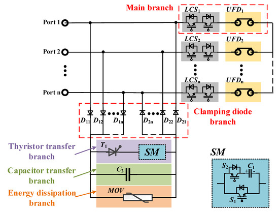
Figure 1.
Topology of the proposed MP-HDCCB.
The main branch: This is composed of an ultra-fast disconnector (UFD) and bidirectional load communication switch (LCS) in series. The bidirectional LCS consists of two IGBT modules in reverse series. In IGBT modules, diodes are antiparallel connected with IGBTs. By turning off the LCS of the corresponding line, the fault current is commutated from the main branch to the transfer branch so as to ensure that the UFD breaks without arc under zero current. When it is necessary to pre-close or reclose the circuit breaker, turn on the bidirectional LCS and turn on each switching device of the transfer branch. If there is no fault current detected in the transfer branch, turn on the UFD to commutate the current to the main branch.
Transfer branch and energy dissipation branch: The transfer branch is made up of the thyristor transfer branch and the capacitor transfer branch. In detail, the thyristor transfer branch is series-connected by the IGBT half-bridge submodule (SM) and T1-thyristor, within which the function of withstanding the high DC voltage is served by thyristors, and the function of the fast breaking fault current is served by SM. The capacitor transfer branch consists of the individual C2 capacitor. The energy dissipation branch is mainly composed of metal-oxide varistors (MOVs), which are used to limit TIV and to absorb the residual energy in the HVDC system. Illustrated in Figure 1 is the internal topology of the IGBT half-bridge submodule (SM). It is worth noting that C1 in SM need be pre-charged; one is to ensure that there is a forward voltage drop when thyristor T1 is turned on, which accelerates the conduction of the thyristor. The other is to use the energy stored by the reverse charging of capacitor C1 to suppress the rise in fault current.
Clamping diode branch: Diode D11…D1n and D21…D2n are connected, respectively, to each end of the transfer branch and then connected to each port. The function of the diode branch is to ensure that the fault current of any port can flow to the transfer branch so as to achieve the purpose of sharing the transfer branch.
2.2. Working Principles of the Proposed MP-HDCCB
Figure 2 shows the working process of fault breaking accomplished by the MP-HDCCB proposed in this paper. The T1 and SM on the transfer branch, during normal working conditions, are both in a closed state; the load current of each port flows through UFDi and LCSi on the main branch connected to every port accordingly; the relevant current flow is shown in Figure 2a. Moreover, the capacitor C1 in the SM of the transfer branch is pre-charged. In the case of ground-fault short circuit happening on a certain line, assuming it is the line on which port 1 locates in Figure 2a, the MP-HDCCB detects the fault and its action process is as follows:
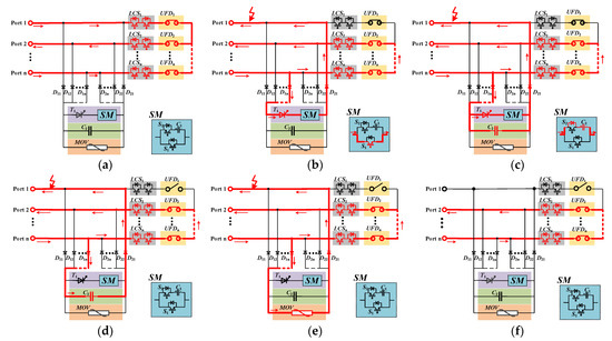
Figure 2.
Current path during the breaking process of the proposed MP-HDCCB. (a) Normal conduction mode. (b) During fault current commutating to S1 of SM. (c) During fault current commutating to C1 of SM. (d) During fault current commutating to C2. (e) During fault current commutating to MOV. (f) After fault breaking of port 1.
(1) As shown in Figure 2b, the LCS1 is commanded to be turned off first. Meanwhile, the thyristor T1 and the IGBT module S1 of SM are turned on immediately in order to force the fault current of port 1 to be commutated to the thyristor transfer branch. By then the load current at port 1 begins to drop. Because C1 has pre-charge voltage, the fault current is commutated to S1, rather than S2.
(2) When the fault current of port 1 is about to reach zero, the UFD1 is turned off. The mechanical switch achieves zero-current and zero-voltage turn-off.
(3) Once the UFD1 is fully turned off, S2 of the SM is commanded to be turned on. In the meantime, the thyristor T1 and S1 of the SM are turned off, forcing the fault current to be commutated to the capacitor transfer branch. Since there is a reverse recovery current during the turn-off process of thyristor T1, this current will reverse charge capacitor C1 in the SM. When the reverse recovery current of T1 drops to 0, the thyristor T1 will withstand the voltage equaling to the difference of C1 and C2. With the purpose of turning off T1 quickly, the voltage across the thyristor T1 needs to constantly maintain the reverse standoff voltage over the period of fault current commutating from the thyristor branch to the capacitor branch. Therefore, the determination of the initial voltage of C1 requires the voltage across C1 to still be higher than the voltage across C2 after the reverse recovery of T1 is finished, keeping the thyristor T1 withstand reverse voltage after the reverse recovery process. Illustrated in Figure 2c is the process of commutating fault current.
(4) As the thyristor T1 is turned off completely, shown in Figure 2d, the fault current is completely commutated to the capacitor branch. The fault current charges C2. When the C2 voltage is bigger than the port 1 voltage, the fault current is beginning to decrease. The blocking time of the fault current is determined by the value of C2; the smaller the value of C2, the smaller blocking time.
(5) As shown in Figure 2e, when the voltage across C2 reaches the clamping voltage of MOV on the energy dissipation branch, the fault current is commutated from the capacitor branch to the energy dissipation branch while the residual energy in the DC system is absorbed by MOV; later on, the fault current decreases gradually. Finally, as shown in Figure 2f, the residual current is interrupted. The fault current is completely isolated by the MP-HDCCB, and port 2 to port n still work normally.
Figure 2 shows that over the action process of the MP-HDCCB, the power exchange of transmission lines between other ports can be carried out through the path of UFD2-LCS2-LCSn-UFDn, ensuring that other normal lines are exempted from the impacts of the fault line and work in a normal state simultaneously. If the current direction of port 1 is reversed and other port current remains unchanged, the diodes D11, D1n and D21 are conductive to provide the fault current path. Diodes D11-D1n and D21-D2n serve the function of achieving bidirectional current flow of MP-HDCCB on each line. The thyristor transfer branch only considers the unidirectional conduction, which will reduce the cost of the transfer branch.
3. Analysis and Parameter Design
3.1. The Major Circuit Parameter Design
The key focus of the parametric design of the proposed topology lies in assuring that the reverse voltage is kept valid over the process of thyristor reverse recovery. When the load current of port 1 exceeds the safety threshold, it commutates from the main branch of port 1 to the branch comprised of diode D1n, thyristor T1, SM (S1) and diode D21 in series; by then the fault current keeps rising. Assuming the duration of such a process is t1, which is mainly used to wait for the UFD1 to turn off completely, the relationship between associated thyristor T1 and the current flowing through port 1 is shown below:
Herein Udc represents the line voltage from port 1 to port n, Ls stands for the line current-limiting inductor and iL(t) is the current at port 1 after the fault occurs. The initial value of fault current, i2, commutating from the thyristor transfer branch to the capacitor transfer branch, can be obtained when ith and t1 are substituted into the calculation. ith is the operation threshold value of MP-HDCCB (initial value of iL(t) in Equation (1)). t1 is the current duration of thyristor transfer branch.
Using the voltage of C2 in the capacitor transfer branch as the calculation target
Substituting into Equation (1)
The results of substituting the initial value and conducting the eigenvalue equation are
The fault current flowing through C2 is
The value of C2 can be obtained via Equation (4) by assuming that the duration of state maintenance is t2 and the clamping voltage of MOV is Umov_th. The C1 of the SM mainly serves the function to provide the thyristor T1 with reverse stand-off voltage over the whole process of fault current commutating from the thyristor transfer branch to the capacitor transfer branch. As shown in Figure 2c, after the S1 of the SM is turned off, the voltage across capacitor C1 is higher than that across C2, which leads the fault current to commutate from the thyristor transfer branch where C1 is located to the capacitor transfer branch where C2 is located. In the meantime, thyristor T1 is not fully turned off. Then, the fault current starts to charge C2 on the capacitor transfer branch during the time when the thyristor undergoes reverse recovery. Over the time period of trec, increase in voltage, UC2s, of the C2 on capacitor transfer branch can be obtained by having the duration of reverse recovery of thyristor T1 (trec) substituted into Equation (4).
In order to make sure thyristor T1 is completely turned off, it is necessary to ensure that the voltage (UC1) across C1 is still higher than that (UC2) across C2 after trec. During trec the charge in thyristor T1 is fully neutralized by C1; hence,
As per Equation (6), the relationships among voltage, capacitance and charge of capacitor C1 are
Assuming a decrease in voltage of C1 is U0 and the reverse charge of the thyristor is Q within trec, the value of capacitance C1 can be calculated by Equation (7). Based on the analysis done above, the initial voltage of C1 needs to be higher than the sum of the voltage required to neutralize the reverse recovery charge and the voltage to charge C2 during the duration of the reverse recovery, namely UC2s + UC1.
The end time point of fault breaking is referred to as the point of time when the current of the fault line at port 1 reaches the peak value and begins to drop. When the voltage across C2 rises to the system voltage, the voltage across the line inductance is 0; by then the line current starts to decrease, deriving from Equation (4)
Thus, the breaking time is
The breaking time and the capacitance C2 can be calculated by substituting system parameters into the present equation.
Taking the practical application of the MP-HDCCB into account, a relatively low value of capacitance C2 indicates a faster speed of breaking fault current, in light of the fact that UC2 is able to increase to Udc more quickly, but at the same time, the voltage of charging C2 (UC2) is rendered too high within the time of the thyristor reverse recovery. Thus, the initial voltage of SM has to be set very high, resulting in the increase in the voltage withstood by IGBT in SM (S1, S2) and the increase in the number of IGBTs required to be series connected, which, in the end, boosts the cost, volume and energy loss. Therefore, the designing stage involves a thorough and in-depth trade-off between breaking time and capacitance according to specific project conditions.
On HVDC transmission lines, the value of capacitance C2, according to the calculations above, is uF level [11], and C1 of the mF-level capacitance value is preferable to make sure the impedance of C2 is far lower than that of C1.
Figure 1 shows a simplified version of typical HCB topology, in the practical engineering application; the thyristor of the thyristor transfer branch is formed by valve groups in series, so the SM needed to be series connected. The thyristor valve groups withstand TIV, and its quantity in series is determined by the line voltage, while the quantity of the SM forming series connection depends on the voltage of C1 derived from Equations (8) and (9). The quantity of the required SM can be obtained once the parameters of thyristors are made sure of, which is the design basis for thyristor series connection and SM series connection under different DC voltage levels.
The energy dissipation branch involves mainly considering the design of two sets of parameters; one is the clamping voltage of MOV and the other is energy required to be absorbed by MOV. The energy dissipation branch involves mainly considering the design of the two sets of parameters; one is the clamping voltage of MOV and the other is the energy required to be absorbed by MOV.
Using fault current iL(t) as the calculation target, the results of the derivation conducted on Equation (4) are
When the energy dissipation branch is conductive, initial fault current i2 can be obtained by substituting t2 into Equation (8). The energy dissipation branch is equivalent to the voltage source of UC2; at this moment the fault current decreases to 0; therefore, the total energy required to be absorbed by the energy dissipation branch consists of two parts: (1) Energy stored by the line inductor at the moment when the branch is conductive; (2) energy offered by port n after the energy dissipation branch is connected, which herein is simplified as power source Udc.
The energy of part (1) is
Over the process of discharging energy by MOV, the decrease in the circuit current can be regarded as a linear relationship. Thus, the time required for the current to drop to 0 is
The energy of part (2) provided by source supply Udc is
Thereby the total energy required to be absorbed by the energy dissipation circuit is
In real application scenarios, the clamping voltage of MOV is usually 1 to 2 times the rated voltage [14]; assuming the clamping voltage of MOV is UC2s = γUdc, at the moment of MOV conduction, there is
The time of the charging capacitor is
within which
As can be seen from Equation (16), setting the clamping voltage of MOV too high results in the rise in the peak voltage of C2, leading to prolonged charging time of capacitor and, furthermore, having the time for the fault current to drop to zero increase after the DC circuit breaker completes the breaking of the fault current, which is followed by an increase in the cost of the capacitor, although the validity of the breaker is not affected.
3.2. Economic Analysis
Figure 3 shows a typical circuit breaker topology [6] when full controlled switching devices are used as main breakers.
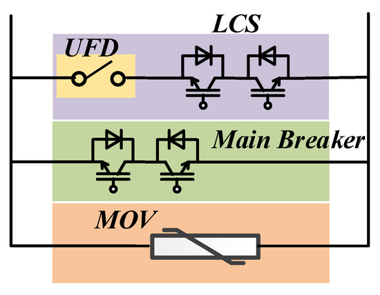
Figure 3.
A typical hybrid DC circuit breaker topology.
Based on this topology, a wealth of IGBTs need to be series connected to withstand TIV, bringing about issues of voltage sharing and current sharing of full controlled devices. Yet in the proposal given in the present study, IGBT only needs to withstand the pre-charge voltage UC1 for the reverse breaking of SCR; this voltage value is significantly lower that system voltage.
Table 1 lists the comparisons done between the quantity of power electronic devices of the present proposal and those using IGBTs as the transfer branch. Herein n stands for the number of SCRs used in the present proposal, m represents the number of IGBTs needed in the present proposal, j represents the number of the port and k is the ratio of system voltage and the pre-charged voltage on C1, which is 500 kV/10 kV = 50 among the system parameters used in the present study. It can be seen that compared with the IGBTs multiport proposal, only one more capacitor and more SCRs are used in the present proposal. Besides, the quantity of IGBTs used in the present proposal is remarkably smaller than that of the scheme in which the transfer branch completely uses the IGBT. The voltage UC2, previously withstood by IGBT when system voltage is exceeded, is now withstood by SCR, leading to a significant decrease in the cost of the present proposal.

Table 1.
Comparison of the number of power electronic devices in different schemes.
In addition, series connection of thyristors is adopted in the proposed topology in the present study to achieve high-voltage application of the DC circuit breaker; IGBT is added to secure fast breaking of thyristors. Hence, in comparison with full controlled switching devices, the overall cost of the proposed topology using a hybrid switching device in the engineering application is going to be lowered significantly.
4. Simulation Results
4.1. System Configuration
In order to further assess the performance of the MP-HDCCB proposed in the present study, four-terminal modular multilevel converter High Voltage DC (MMC-HVDC) test system models are built in this section. Herein the voltage of station 2 reaches 500 kV, the rated capacities of P1, P3 and P4 reach 500 MW, 750 MW and 750 MW, respectively. Figure 4 shows the locations where MP-HDCCBs are equipped and the location where the fault happens. The parameters of the simulation model system are shown in Table 2.
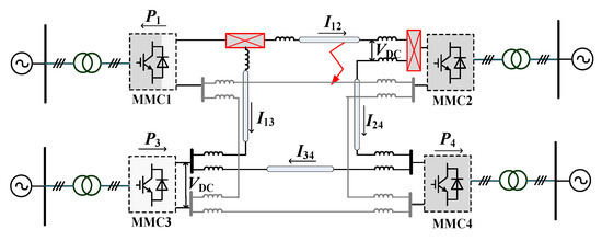
Figure 4.
Schematic diagram of four-terminal test system with MP-HDCCB.
Table 2.
The parameters of the simulation model system.
4.2. Simulation of Fault Isolation
Figure 5 shows the currents flowing on different branches; a short-circuit fault occurs on line MMC1-MMC2 when t = t0 = 3 s; the current flowing through main branch rises rapidly. When the fault is detected after 1 ms, T1 is turned on and S1 is opened; then the LCS1 is open; the fault current commutates from the main branch to the transfer branch and keeps rising. At this moment, the mechanical switch UFD1 begins to open in zero current. After a delay of 2 ms, UFD1 is fully open. S2 is turned on so that the UC1 provides a reverse voltage on T1, having T1 turned off; thus, the fault current commutates to C2 quickly, over which the fault current reaches the peak value of 11 kA. The fault current keeps charging C2 till the voltage across C2 exceeds the clamping voltage of MOV and commutates to the energy dissipation branch. Afterwards, the fault current declines to 0; hereby the fault is completely interrupted.
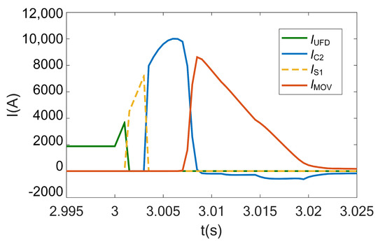
Figure 5.
Current curve of each branch of MP-HDCCB during fault breaking.
Figure 6 shows the voltages of major components over the process of breaking fault current. The voltage across the DC circuit breaker is suppressed by MOV. The clamping voltage of the MOV set in present proposal is 50% higher than the rate line voltage of system.
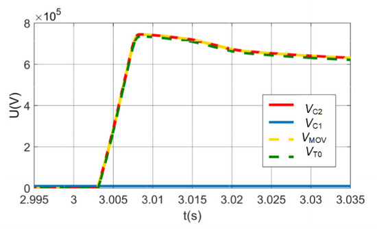
Figure 6.
The voltages of major components over the process of breaking fault current.
Figure 7 shows the port currents of the four-terminal test system; the fault happens on line MMC1-MMC2 when t is equal to 3 s. It can be observed from Figure 7 that, after the MP-HDCCB at both ends of line MMC1-MMC2 completes breaking, the power supply on the other normal lines has not been impacted.
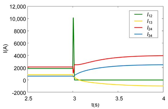
Figure 7.
Port currents of the four-terminal test system.
4.3. Parameter Influence Analysis
Figure 8 shows the effects of different capacitance values of C2 on the current flowing through the transfer branches and the voltage across C2; the results indicate that the lower the capacitance value is, the faster the voltage of the capacitor rises, the quicker the MOV conducts and the lower the current peak value is. However, UC2 needs to be large enough because the breaking condition of T1 requires UC1 to be higher than UC2. The time of thyristors withstanding reverse voltage is set at 70 us; namely, UC1 is higher than UC2 within the temporal range of 70 us. Figure 9 depicts the corresponding pre-charge voltage of C1 required for different capacitance values.
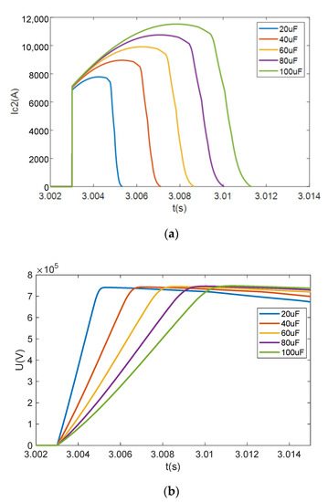
Figure 8.
The effects of different capacitances of C2 on the current flowing through the transfer branch and the voltage across C2. (a) Current curve flowing through the transfer branch under different capacitances. (b) Voltage curve across C2 under different capacitances.
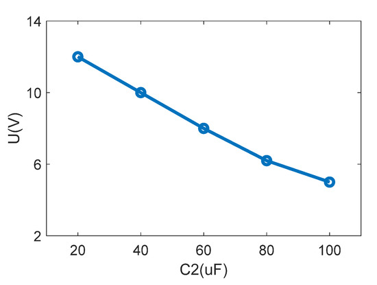
Figure 9.
The corresponding pre-charge voltage of C1 required for different capacitance values.
Under the conditions that the C2 on the capacitor transfer branch is 50 uF and the MOV protection factors are different, the changes in current flowing through the MP-HDCCB and voltage across MOV are shown in Figure 10. It can be seen that the clamping voltage of MOV does not affect the rising time of the fault current (the breaking time of the fault current) when other parameters remain unchanged, but the time for the fault current to drop to zero is influenced. In addition, it can be concluded that the higher the clamping voltage of MOV is, the shorter of the time for the current to drop to zero, the less energy that MOV needs to absorb and the shorter the time for circuit breakers to reclose. However, a too high clamping voltage of MOV results in capacitors withstanding higher voltage, which is true for series thyristors as well, giving rise to an increase in the cost and volume of switching devices. Therefore, the clamping voltage of the MOV should be selected based on proper integration of these two factors.
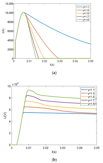
Figure 10.
Comparison of different clamping voltages of MOV. (a) Fault current curves under different clamping voltages of MOV. (b) Voltage curves under different clamping voltages of MOV.
5. Experiment Results
The proposed MP-HDCCB was established in our laboratory according to the topology shown in Figure 1, and a scaled-down test circuit was constructed, as shown in Figure 11, to verify the effectiveness of the proposed MP-HDCCB. The parameters of the test circuit are listed in Table 3.
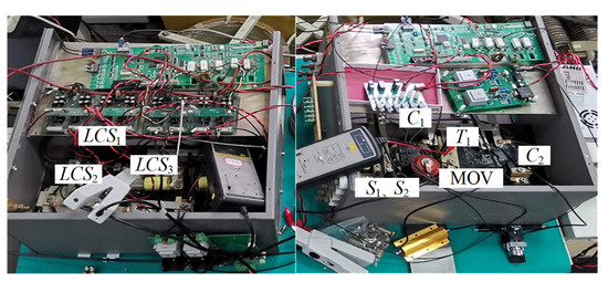
Figure 11.
Photograph of the scaled-down experiment test circuit.
Table 3.
Major parameters of test circuit.
Figure 12 shows the fault current blocking waveform after the fault occurs at port 1. The current of the main branch begins to rise at time t1. The IGBT of the main branch is turned off at t2. The fault current is commutated to the thyristor branch and the fault current increases continuously. The IGBT of the thyristor branch is turned off at t3. The fault current is commutated to the capacitor branch and C2 is charged. When the voltage on C2 is higher than the line voltage, the fault current of the capacitor branch begins to decrease until the fault current is completely interrupted. The time from t1 to t2 is the fault current blocking time, which is the key index for the DC breaker. The blocking time of the experiment is 3 ms because achieving the threshold current value needs 1 ms and waiting for the mechanical switch to shut down needs 2 ms.
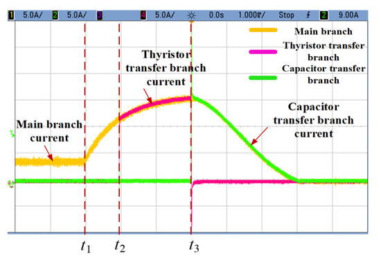
Figure 12.
Photograph of the scaled-down experiment test circuit.
The waveform after magnifying the time scale at t3 in Figure 12 is shown in Figure 13. The IGBT of the thyristor branch turns off at t3. C1 has an initial pre-charged voltage, which causes the thyristor withstand reverse voltage at t3. The current through the thyristor branch is commutated to the capacitor branch while the current through the capacitor branch increases rapidly. The voltage of C1 must be greater than the voltage of C2 at t4 to ensure that the thyristor is able to withstand the reverse stand-off voltage during its reverse recovery process. When the thyristor is turned off, the current is completely commutated to the capacitor branch and the fault current starts to charge C2 of the capacitor branch.
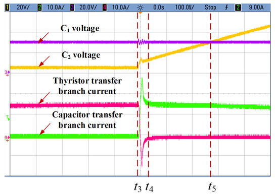
Figure 13.
Photograph of the scaled-down experiment test circuit.
Adjusting the value on C2 to 100 uF, and the fault current blocking process is shown in Figure 14. The fault current is normally commutated to the thyristor branch at t2. However, the current of the thyristor branch is not completely commutated to the capacitor branch at t3. After the thyristor is turned off, the thyristor is turned on again, resulting in the current of the thyristor branch rising to the line current again. Figure 15 shows a detailed view of the enlarged time scale at t3 in Figure 14.
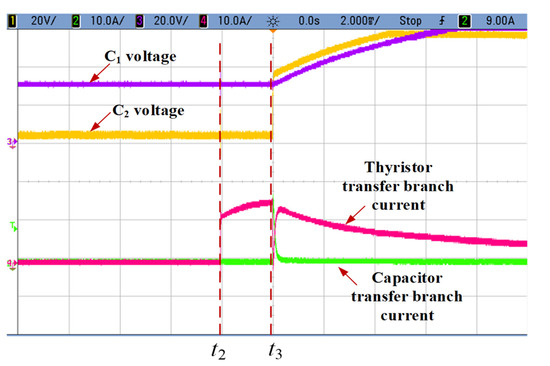
Figure 14.
Test result of failing to block fault current.

Figure 15.
Test result of failing to block fault current.
The thyristor is turned off and the thyristor branch current begins to decrease at t3 along with the fault current charges C2. However, since the value of C2 is too small, the voltage on C2 was higher than the voltage on C1 at t3-1 while the thyristor began to withstand the forward voltage before the end of the reverse recovery process. The thyristor was restored to the conductive state, and the current was commutated back to the thyristor branch, causing the failure of fault current interruption.
The proposed MP-HDCCB topology in a practical engineering application is shown in Figure 16. The thyristor transfer branch, which is formed by thyristor and SM, needs to withstand DC bus voltage. Because the cost and difficulty of the thyristor series is smaller than the SM series, the thyristor series is used to withstand the high voltage and the SM is used to turn off the current quickly. The thyristor series scheme is in widespread use [22,23,24]; the proposed topology reliability could be assured. The pre-charge voltage of C1 is still satisfied concerning Equations (6) and (7), and the reverse charge Q is the sum of thyristor T1 − Tn.

Figure 16.
Topology of the proposed MP-HDCCB in practical engineering application.
6. Conclusions
A multiport hybrid DC circuit breaker topology based on hybrid switching devices was proposed in the present study; comparisons of performance between the proposed topology in this study and a conventional scheme involving multiport hybrid DC circuit breakers were conducted, and the conclusions are as follow:
(1) The working principles and parameters of the proposed MP-HDCCB were studied and analyzed. It was concluded that this proposed scheme is capable of breaking the fault current reliably and isolating faults without impacting the normal operation of other lines.
(2) The proposed MP-HDCCB only needs one thyristor transfer branch, one capacitor transfer branch and one energy dissipation branch. The current of the thyristor transfer branch is unidirectional conduction, and the bidirectional fault current is solved by the clamped diode.
For the unidirectional current blocking, the scheme adopts full controlled switching devices in the thyristor transfer branch to ensure the rapidity of the breaking current, and the semi-controlled switching devices are connected in series to withstand TIV. According to the multiplexing transfer branch, unidirectional conduction and semi-controlled switching, the quantity of the full controlled switching devices is significantly reduced, showing a certain degree of application value in lowering the relevant project cost and technical difficulty.
(3) In order to turn off the thyristor, the capacitance value and pre-charge voltage should be configurated effectively to solve the problem of thyristor reverse recovery.
Author Contributions
H.J. conceived and designed the study. J.Y., T.W. and J.L. given suggestions, J.Z. and Z.Y. revised the manuscript. All authors have read and agreed to the published version of the manuscript.
Funding
This research work was funded by the National Natural Science Foundation of China under Grant 61972398, in part by the Institute of Electrical Engineering, CAS(E155610201), in part by Natural Science Foundation of Jiangsu Province BK20210048 and in part by Youth Innovation Promotion Association(2020144).
Conflicts of Interest
The authors declare no conflict of interest.
References
- Ahmed, N.; Ängquist, L.; Mahmood, S.; Antonopoulos, A.; Harnefors, L.; Norrga, S.; Nee, H.-P. Efficient Modeling of an MMC-Based Multiterminal DC System Employing Hybrid HVDC Breakers. IEEE Trans. Power Del. 2015, 30, 1792–1801. [Google Scholar] [CrossRef]
- Wang, S.; Ugalde-Loo, C.E.; Li, C.; Liang, J.; Adeuyi, O.D. Bridge-Type Integrated Hybrid DC Circuit Breakers. IEEE Trans. Emerg. Sel. Topics Power Electron. 2020, 8, 1134–1151. [Google Scholar] [CrossRef]
- Liu, G.; Xu, F.; Xu, Z.; Zhang, Z.; Tang, G. Assembly HVDC breaker for HVDC grids with modular multilevel converters. IEEE Trans. Power Electron. 2017, 32, 931–941. [Google Scholar] [CrossRef]
- Hassanpoor, A.; Häfner, J.; Jacobson, B. Technical Assessment of Load Commutation Switch in Hybrid HVDC Breaker. IEEE Trans. Power Electron. 2015, 30, 5393–5400. [Google Scholar] [CrossRef]
- Franck, C.M. HVDC circuit breakers: A review identifying future research needs. IEEE Trans. Power Deliv. 2011, 26, 998–1007. [Google Scholar] [CrossRef] [Green Version]
- Zhu, J.; Liu, D.; Yin, J.; Wei, T. Research on Hybrid DC Breaker Based on Modular Cascaded Structure. In Proceedings of the 2nd World Congress on Civil, Structural, and Environmental Engineering, Barcelona, Spain, 2–4 April 2017; Volume 37, pp. 1560–1567. [Google Scholar]
- Yan, J.; Xu, J.; Zhao, C. A Review of Design Methods for Energy Absorption Path Design in High Voltage Direct Current Circuit Breakers. In Proceedings of the 4th World Congress on Civil, Structural, and Environmental Engineering (CSEE’19), Rome, Italy, 7–9 April 2019; Volume 39, pp. 4301–4315. [Google Scholar]
- Li, C.; Liang, J.; Wang, S. Interlink Hybrid DC Circuit Breaker. IEEE Trans. Ind. Electron. 2018, 65, 8677–8686. [Google Scholar] [CrossRef]
- Hao, C.; Qin, Y.; Hua, H. Energy “Routers”, “Computers” and “Protocols”. In Energy Internet; Springer: Berlin/Heidelberg, Germany, 2020. [Google Scholar]
- Shi, Z.; Zhang, Y.; Jia, S.; Song, X.; Wang, L.; Chen, M. Design and numerical investigation of a HVDC vacuum switch based on artificial current zero. IEEE Trans. Dielectr. Electr. Insul. 2015, 22, 135–141. [Google Scholar] [CrossRef]
- Grieshaber, W.; Violleau, L. Development and test of a 120 kV direct current circuit breaker. Proc. CIGRÉ Sess. Paris Fr. 2014, 14, 111. [Google Scholar]
- Callavik, M.; Blomberg, A.; Jafner, J.; Jacobson, B. The hybrid HVDC breaker:An innovation breakthrough enabling reliable HVDC grids. ABB Grid Syst. 2012, 14, 7–13. [Google Scholar]
- Majumder, R.; Auddy, S.; Berggren, B.; Velotto, G.; Barupati, P.; Jonsson, T.U. An Alternative Method to Build DC Switchyard With Hybrid DC Breaker for DC Grid. IEEE Trans. Power Deliv. 2017, 32, 713–722. [Google Scholar] [CrossRef]
- Zhang, S.; Zou, G.; Wei, X.; Sun, C. Diode-Bridge Multiport Hybrid DC Circuit Breaker for Multiterminal DC Grids. IEEE Trans. Ind. Electron. 2021, 68, 270–281. [Google Scholar] [CrossRef]
- Kontos, E.; Schultz, T.; Mackay, L.; Ramirez-Elizondo, L.M.; Franck, C.M.; Bauer, P. Multiline Breaker for HVDC Applications. IEEE Trans. Power Deliv. 2018, 33, 1469–1478. [Google Scholar] [CrossRef]
- Belda, N.A.; Plet, C.A.; Smeets, R.P.P. Analysis of faults in multiterminal HVDC grid for definition of test requirements of HVDC circuit breakers. IEEE Trans. Power Deliv. 2018, 33, 403–411. [Google Scholar] [CrossRef]
- Koyama, Y.; Morikawa, R.; Ishiguro, T. Multiline Hybrid DC Circuit Breaker with Low Conduction Loss and Reduced Semiconductor Breaker. In Proceedings of the 21st Conference on Power Electronics and Applications (and Exhibition), EPE’19 ECCE (Energy Conversion Congress and Expo) Europe, Genova, Italy, 2–6 September 2019; pp. 1–10. [Google Scholar]
- Mokhberdoran, A.; Van Hertem, D.; Silva, N.; Leite, H.; Carvalho, A. Multiport hybrid HVDC circuit breaker. IEEE Trans. Ind. Electron. 2018, 65, 309–320. [Google Scholar] [CrossRef] [Green Version]
- Liu, W.; Liu, F.; Zha, X.; Chen, C.; Yu, T. A topology of the multi-port DC circuit breaker for multi-terminal DC system fault protection. In Proceedings of the 2017 IEEE Energy Conversion Congress and Exposition (ECCE), Cincinnati, OH, USA, 1–5 October 2017; pp. 3760–3763. [Google Scholar]
- He, J.; Luo, Y.; Li, M.; Zhang, Y.; Xu, Y.; Zhang, Q.; Luo, G. A High-Performance and Economical Multiport Hybrid Direct Current Circuit Breaker. IEEE Trans. Ind. Electron. 2020, 67, 8921–8930. [Google Scholar] [CrossRef]
- Liu, W.; Liu, F.; Zhuang, Y.; Zha, X.; Chen, C.; Yu, T. A Multiport Circuit Breaker-Based Multiterminal DC System Fault Protection. IEEE J. Emerg. Sel. Topics Power Electron. 2019, 7, 118–128. [Google Scholar] [CrossRef]
- Jamshidifar, A.; Jovcic, D. Design, modeling and control of hybrid DC circuit breaker based on fast thyristors. IEEE Trans. Power Deliv. 2018, 33, 919–927. [Google Scholar] [CrossRef] [Green Version]
- Shu, J.; Ma, J.; Wang, S.; Dong, Y.; Liu, T.; He, Z. A New Active Thyristor-Based DCCB With Reliable Opening Process. IEEE Trans. Power Electron. 2021, 36, 3617–3621. [Google Scholar] [CrossRef]
- Dongye, Z.; Qi, L.; Cui, X.; Qiu, P.; Lu, F. A New Approach to Model Reverse Recovery Process of a Thyristor for HVdc Circuit Breaker Testing. IEEE Trans. Power Electron. 2021, 36, 1591–1601. [Google Scholar] [CrossRef]
Publisher’s Note: MDPI stays neutral with regard to jurisdictional claims in published maps and institutional affiliations. |
© 2022 by the authors. Licensee MDPI, Basel, Switzerland. This article is an open access article distributed under the terms and conditions of the Creative Commons Attribution (CC BY) license (https://creativecommons.org/licenses/by/4.0/).