Abstract
The main goal of this work was to conduct a comparative analysis of the electrical properties of the silicon implanted with neon ions, depending on the dose of ions and the type of substrate doping, for the possibility of generating additional energy levels by ion implantation in terms of improving the efficiency of photovoltaic cells made on its basis. The article presents the results of research on the capacitance and conductance of silicon samples doped with boron and phosphorus, the structure of which was modified in the implantation process with Ne+ ions with energy E = 100 keV and different doses. The analysis of changes in electrical properties recorded at the annealing temperature of the samples Ta = 298 K, 473 K, 598 K, 673 K, and 873 K, concerned the influence of the test temperature in the range from 203 K to 373 K, as well as the frequency f from 100 Hz to 10 MHz, and voltage U from 0.25 V to 2 V. It was possible to detect intermediate bands in the tested samples and determine their position in the band gap by estimating the activation energy value. By means of implantation, it is possible to modify the width of the silicon energy gap, the value of which directly affects the efficiency of the photovoltaic cell made on its basis. By introducing appropriate defects into the silicon crystal lattice, contributing to a change in the value of the energy gap Eg, it is possible to increase the efficiency of the solar cell. On the basis of the obtained results, it can be seen that the highest activation energies are achieved for samples doped with phosphorus.
1. Introduction
The need to switch to available forms of renewable energy is now a key topic that will allow a gradual withdrawal from conventional energy based on fossil sources. One of the options for using renewable energy sources is to convert energy from solar radiation into electricity [1,2,3,4]. Photovoltaic cells, as the most popular solar energy conversion devices, have already been extensively tested to improve efficiency and safety, and to reduce energy production costs. The efficiency of this conversion is the most important factor determining the efficiency of the cells. Currently, manufacturers in the photovoltaic industry have the task of lowering the price of solar cells and increasing their efficiency [5,6,7,8].
The main industrial goal of generating energy from renewable sources using photovoltaic cells is the reduction of the cost of generating electricity compared to commercial electricity drawn from the power grid [9]. This includes cost reduction at all stages of manufacturing these devices, starting from material production, production of photovoltaic (PV) cells, and entire modules or panels, system installation, while maintaining maximum cell conversion efficiency. According to estimates, as much as half of the price of the entire photovoltaic module is related to the production of the base material, crystal growth, and the creation of silicon wafers, while the other half comes from cell processing and module assembly [10]. Better use of silicon during the manufacturing process will reduce the cost of the cell. For example, in the case of crystal formation where there is no need to cut the material, most of the silicon is consumed. However, the disadvantage of this method is the lower yield due to the lower quality of the material, as well as the greater number of defects due to thermal stresses during the growth process, which shortens the life of the base material. Another example is back contact silicon PV cells as high efficiency devices in which all metallization on the front surface is removed. This reduces optical losses, such as shading and reflection losses [11].
The dynamic development of the production of photovoltaic cells and numerous research works on the production technology are currently focused mainly on third generation cells [12,13,14]. Third generation solar cell concepts have recently been explored to improve the performance of solar cells above the current limit [15], based on a chart of the highest confirmed conversion efficiencies for research cells for a range of photovoltaic technologies, from 1976 to the present, according to the National Renewable Energy Laboratory [16]. The highest efficiency is achieved by cells made in experimental technologies, first generation cells based on silicon achieve up to 27.6% efficiency [16], second generation CIGS or CdTe cells have efficiency of 23.4% [16], and third generation cells based on innovative materials: perovskite cells, dye sensitized or organic cells, the value is 29.1% [16]. The highest efficiency of 47.1% [16] has heterojunction cells and intermediate band solar cells (IBSCs), the main feature of which is an additional intermediate band in the silicon band structure model [16]. Increasing the efficiency of traditional solar cells depends on the use of appropriate band gap materials and a high-quality device. Third generation solar cells are based on novel principles that can only be realized with specially designed materials. This in turn forces the production of new materials, a combination of different structures that lead to new phenomena of photoconversion [17]. There are two basic aspects of third generation photovoltaic cells. The first is new physical mechanisms of sunlight conversion. They are aimed at better understanding and mastering the fundamental phenomena governing photovoltaic conversion and limiting the quantum efficiency of solar cells. The combination of optical spectroscopy and electric transport technology allowed to investigate the physical phenomena responsible for photoconversion [18]. Their main goal is to determine the presence of new phenomena such as impurity photovoltaic effect (IPV) and intermediate band generation (IBSC). Another aspect of the third generation of cells is the production of new materials and their various combinations. The aim is to obtain materials representing the physical phenomena required for third generation solar cells, but with even better performance. By analyzing the engineering aspects of these technologies and identifying unique capabilities, it was possible to improve efficiency and reduce costs [19].
One way to increase efficiency is to create additional energy levels. The work carried out for many years by our research team in this area has allowed us to gather experience in this field, which has been quoted in numerous articles [20,21,22,23].
The impurity photovoltaic effect (IPV) is one of the concepts used to increase the efficiency of photovoltaic cells. The idea of the IPV effect is based on the introduction of deep defects into the solar cell, which provide a multi-stage absorption mechanism for the photons in the band gap to create new electron-hole pairs. The dominant loss mechanisms in conventional PV cells are the inability to absorb photons and the photons releasing some of their energy to the lattice in the form of heat. The third generation solar cell concept aims to solve these two problems, making it possible to use the full spectrum by incorporating new mechanisms to create new electron-hole pairs [24]. The impurity photovoltaic effect is one of the concepts that is based on the incorporation of optically active defects into the cell. These defects create additional energy levels in the band gap that can create new free carriers by absorbing low-energy photons. This effect can improve the efficiency of solar cells. Studies on the impact of IPV were theoretically and experimentally performed on silicon and GaAs-based solar cells [25]. The challenge is to find the right impurity, structure and material to be able to fulfill certain strict assumptions placed on the atoms or structure of IPV. Recent studies by the research team has shown that IPV defects must be relatively far from the center of the band gap of the base material. It has long been known that middle gap impurities are responsible for radiative recombination and, therefore, act as recombination centers instead of useful impurities. It has been confirmed that the improvement of the parameters of crystalline silicon solar cells is possible by selecting a structure with a Back Surface Field (BSF) layer [26].
The idea of an intermediate band solar cell (IBSC) is to absorb photons with energy below the band gap to generate electricity. These photons are absorbed by a semiconductor material that, in addition to the conduction and valence bands, shows an intermediate band (IB) within the conventional semiconductor band gap [27].
Effective methods of reducing quantum losses are still in the phase of laboratory experiments. However, the key to achieving this goal will be the use of ion implantation. The IBSC cells belonging to the third generation of solar cells represent the greatest potential in this field. They are characterized by an intermediate energy band in the silicon band structure (although the idea of IBSC cells is not limited to silicon as the base material). Many studies have shown [28,29], that the implantation of a high resistivity silicon substrate with titanium ions in selected cases contributes to a significant increase in the absorption of photons whose energy is below the band gap width. The titanium ion implantation of the silicon substrate is aimed at the implementation of theoretical assumptions regarding the construction and structure of IBSC intermediate band photovoltaic cells, according to which the efficiency limit of such a cell is 63.2% [27], which is much higher than the limit of 47.1% [16] for conventional research solar cells with a single energy gap (Multijunction (4-junction or more, Concentrator)) [30].
To achieve maximum efficiency, the total cell band gap should be around 2 eV, due to the Shockley–Queisser limit. However, this fact does not prevent other cells based on different semiconductor materials from benefiting from the presence of an intermediate band (IB) within the band. Since silicon, with a band gap of 1.12 eV, is the dominant material in solar cell technology, the focus of the research is on determining the performance limit of IBSC silicon, because even a small increase in efficiency can cause great commercial interest if the intermediate band can be produced at low cost [31].
Doping of semiconductors can be performed, among others during crystal growth. The conductivity of the absorber is given to the plates at the stage of crystallization, while the production of the emitter layer is a separate process that uses ion implantation or diffusion. In the contrary to doping during crystal growth, in the modern semiconductor industry doping is performed on a substrate (after crystal growth and cutting) to control doping in specific areas by masking undesirable areas [9]. In amorphous silicon cells, the doping is still carried out during deposition. There are three techniques for creating a p–n junction on a silicon substrate: diffusion, ion implantation, and alloy doping. In today’s technology, alloying is rarely used due to anomalies in the electrical properties [9,32].
Ion implantation, which is the second method of doping, can be used to create cells of standard construction, but also more complex structures thanks to very precise introduction of dopants. When using the implantation process, plasma etching of the wafers becomes unnecessary, but instead it is necessary to heat the silicon wafers at high temperatures. This process is aimed at reducing the impact of radiation defects caused by high-energy ions that destroy the structure of the material [33]. By using the implantation process for less complex structures, it is easier to achieve a low surface dopant concentration and to regulate the uniformity of dopant distribution in a more precise way [34].
Recently, the ion implantation technique has gained popularity in the solar industry, slowly replacing the diffusion technique that has been used for many years, so that the efficiency of cells improves with the continuous development of technology. In addition to localized and pattern doping, the main advantages of this technique are: high, precise control of the amount and dose distribution of the dopant, resulting in high homogeneity, reproducibility and increased efficiency, with a much narrower distribution of cell efficiency [9,26].
In the ion implantation method, selected ions of a given dopant are introduced into the semiconductor, accelerating them to a high energy level and implanting them into the semiconductor [35]. The energy transferred to the dopant ions determines the depth of their deposition in the implanted semiconductor. In contrast to the diffusion technique (in which the dose of dopant ions is introduced only to the surface), in the ion implantation technique, a controlled dose of ions can be introduced deep into the semiconductor. This technique provides higher efficiency and lowers costs, not only by improving the technology and increasing the precision of doping, but also by shortening the individual stages of cell manufacturing [36].
Ion implantation is a method that allows the production of advanced silicon structures for photovoltaic applications on a mass scale. The use of implantation significantly simplifies the production process of PV cells, while silicon cells produced using the above-mentioned process achieve the highest efficiency. The main advantage of implantation is the possibility of its multiple use on one production line. Another important aspect is the possibility of modifying the properties of silicon through the appropriate selection of implantation and annealing parameters, which is necessary to reduce the share of radiation defects affecting the efficiency of the cells. [37].
Based on the above considerations, it is justified to continue research on the use of ion implantation in order to improve the resultant efficiency of silicon-based photovoltaic cells. The structures of IBSC in particular seem very interesting, but the selection of the appropriate material in terms of meeting the theoretical assumptions of this structure requires many more experiments, but the ion implantation process will be key to achieving this goal [38].
2. Materials and Methods
In order to obtain data on the potential use of implantation with neon ions, n- and p-type silicone used in the production of PV cells, experimental studies were carried out in the aspect of generating intermediate energy levels in order to improve their efficiency. The research task was to check whether the defects in the silicon crystal lattice caused by neon ion implantation can be used to reduce quantum losses in PV cells by forming structures that meet the IBSC concept.
Taking into account the available literature on the production and characteristics of monocrystalline silicon solar cells, the development process and the procedure for the production of photovoltaic cells were characterized, among others, by the following parameters: n-type silicon cells with crystal orientation (100), resistivity 1.5 Ωcm, thickness 200 μm and diameter 40 mm used as a substrate for the production of solar cells were doped with boron using conventional thermal diffusion [33]. Another exemplary type are wafers with similar geometric dimensions (thickness 200 μm, diameter 40 mm), made of p-type monocrystalline silicon, resistivity 10 Ωcm, crystallographic orientation (111) doped with phosphorus [39].
The analysis of the cell manufacturing procedures allowed to select the research material, which was the commonly used n-type and p-type monocrystalline silicon, doped with boron and phosphorus with the following parameters:
- Boron-doped silicon with resistivity ρ = 10 Ωcm, implanted with Ne+ ions with energy E = 100 keV and doses D = 4 × 1013 cm−2 and 4 × 1014 cm−2;
- Phosphorus-doped silicon with resistivity ρ = 10 Ωcm, implanted with Ne+ ions with energy E = 100 keV and doses D = 4 × 1013 cm−2 and 4 × 1014 cm−2.
Neon ions were selected in the implantation process because they generate mainly point defects, the introduction of which into the silicon crystal lattice allows to change the resistivity or the band gap width, which are basic electrical properties that have a significant impact on internal losses in PV cells. Neutral neon ions do not introduce additional polarization, but their task is to introduce appropriate defects into the structure of silicon [40].
Selected samples of silicon were tested in order to determine the optimal parameters of implantation and the tested material, in terms of creating structures that would improve the efficiency of solar cells made on their basis. The conditions for measuring electrical parameters, such as capacitance and conductance, were determined by the test signal parameters—frequency and voltage—as well as by the instantaneous operating temperature of the tested sample. The results of the measurements were recorded for operating temperatures ranging from 203 K to 373 K with a step of 10 K after forcing a signal in the circuit with a frequency ranging from 100 Hz to 10 MHz and a voltage in the range (0.25–2) V.
Between each measuring cycle, the samples were heat treated by isochronous annealing. This means that the samples were heat treated at the following temperatures Ta: 298 K, 473 K, 598 K, 673 K, and 873 K. The heating process lasted 15 min each time. For the sample with an annealing temperature Ta = 298 K, measurements were made for temperatures in the (203–303) K range, so as not to introduce the effect of additional annealing. Based on the results of research works [2,14,20], the upper limit of annealing of the tested samples was set at 873 K. Exposing the samples to thermal treatment at higher temperatures causes a complete disappearance of defects resulting from ion implantation in the silicon structure.
The laboratory stand for measuring the electrical properties of ion-implanted silicon, consisting of the Discovery DY600C climatic chamber with a special set of measuring holders, 10 MHz Precision LCR Meter and Lutron TM-917 and Fluke 289 temperature meters, have already been described in detail in previous works, as well as the process of preparing the material for testing or recording the results [41].
Four samples with different properties were tested for the effect of ion implantation on the electrical parameters of silicon. During the work, they were assigned names in order to make their identification easier:
- Si01—boron-doped silicon Si+B (p), substrate resistivity ρ = 10 Ωcm, implantation with Ne+ ions with energy E = 100 keV and dose D = 4 × 1013 cm−2.
- Si02—boron-doped silicon Si+B (p), substrate resistivity ρ = 10 Ωcm, implantation with Ne+ ions with energy E = 100 keV and dose D = 4 × 1014 cm−2.
- Si03—phosphorus-doped silicon Si+P (n), substrate resistivity ρ = 10 Ωcm, implantation with Ne+ ions with energy E = 100 keV and dose D = 4 × 1013 cm−2.
- Si04—phosphorus-doped silicon Si+P (n), substrate resistivity ρ = 10 Ωcm, implantation with Ne+ ions with energy E = 100 keV and dose D = 4 × 1014 cm−2.
Based on the results of testing the above samples, the analysis of the effect of the ion dose on the measured electrical parameters—in this case on the capacitance and conductance—was performed. Due to the use of two different dopants, boron and phosphorus, while maintaining the same substrate resistivity, it was possible to determine the effect of the type of dopant on the conductance and capacitance.
Based on the obtained results, with the help of the Grapher software, graphs of capacitance and conductance as a function of temperature of the tested sample were developed, which enabled the analysis of the influence of ion implantation and post-implantation annealing on the electrical parameters of the tested silicon.
3. Results and Discussion
3.1. The Influence of Measurement Conditions on the Tested Electrical Quantities
The conditions for measuring the conductance and capacitance were determined, among others, by the frequency and voltage of the measuring signal. The forced signal in the measuring circuit was characterized by a voltage in the (0.25–2) V range and a frequency in the 100 Hz to 10 MHz range. The influence of the presented conditions on the obtained results has been discussed on the basis of the charts below.
Figure 1 shows the temperature dependences of capacitance and conductance for the Si01 sample, heated at Ta = 598 K. The increase in the measuring temperature in each case contributes to the increase in both the capacitance and the conductance values. The capacitance for the lowest signal frequencies is characterized by large changes in its value, especially for operating temperatures from 203 K to about 250 K. Moreover, the capacitance curves for lower frequencies are characterized by greater changes in the entire temperature range Tp. For a signal with a frequency of 1 kHz, the capacitance varies from approximately 10−9 F to approximately 7 × 10⁻⁹ F. For high signal frequencies with an accuracy of 0.1% over the entire measuring range, the capacitance changes are smaller (from 8 × 10⁻¹⁰ F to 3 × 10⁻⁹ F for 1 MHz). The frequency thus stabilizes the capacitance in the entire tested range of the sample operating temperature.
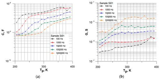
Figure 1.
The dependencies C = f(Tp) (a) and G = f(Tp) (b) for boron-doped silicon with substrate resistivity of ρ = 10 Ωcm, implanted with Ne+ ions with a dose of D = 4 × 1013 cm−2 (Sample Si01) and an annealing temperature Ta = 598 K, recorded for the voltage of the measurement signal U = 2 V.
The conductance values range from 4 × 10⁻⁷ S up to approximately 4 × 10⁻³ S with an accuracy of 0.1% over the entire measuring range, depending on the frequency value of the measuring signal. However, it can be noticed that the course of the conductance looks different for higher measurement temperatures depending on the frequency. The increase in frequency causes a shift in the point where the conductance value begins to stabilize. For the frequency of 1 kHz, this point appears for the temperature of approximately 230 K, while for the frequency of 1 MHz, the beginning of the inhibition of the increase in conductance is visible for the temperature of 300 K.
In comparison to the previous graphs showing the capacitance curve, some differences can be noticed in the above (Figure 2). The dependencies in Figure 2 were made for the measurement results of the Si03 sample, doped with phosphorus, not boron as in the previous cases. However, the change in doping does not affect the general relationship that the higher frequency contributes to the stabilization of the capacitance across the entire operating temperature range. In the presented dependence C = f(Tp) for frequencies in the range of up to 1 kHz, a stage is visible for measuring temperatures above 330 K, where the capacitance remains almost constant. Unlike in the case of boron-doped samples, for lower working temperatures of the sample we have a much narrower range of the achieved capacitance values—e.g., for the initial temperature of 203 K, the measured capacitance for each frequency ranges from approximately 5 × 10⁻¹⁰ F to approximately ok. 9 × 10⁻¹⁰ F. For a sample doped with boron with the same resistivity, the capacitance range for the mentioned temperature is from 8 × 10⁻¹⁰ F to approximately 2 × 10⁻⁹ F.
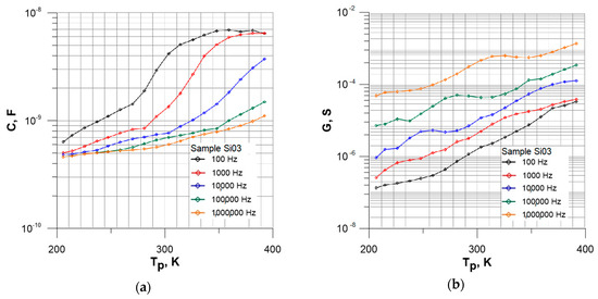
Figure 2.
The dependencies C = f(Tp) (a) and G = f(Tp) (b) for phosphorus-doped silicon with substrate resistivity of ρ = 10 Ωcm, implanted with Ne+ ions with a dose of D = 4 × 1013 cm−2 (Sample Si03) and an annealing temperature Ta = 598 K, recorded for the voltage of the measurement signal U = 2 V.
The conductance over the entire measuring temperature range shows an increase in value. Its highest values were recorded for the highest measurement frequencies. There are three stages in the course of conductance that have different positions in relation to the x-axis depending on the measuring frequency. On the basis of the dependence G = f(Tp) for 10 kHz, the first stage of increasing the conductance value is visible for temperatures (203–240) K. Then, the stabilization stage is visible, and then, above 280 K, the conductance value increases again.
The above graphs showing the temperature dependence of capacitance and conductance showed that frequency can have a significant influence on the measurement results. All of the presented graphs were created for one constant voltage value of the measurement signal equal to U = 2 V. An increase in the frequency value has the effect of smoothing out the course of the capacitance over the entire measuring temperature range. Moreover, for higher frequencies (over 10 kHz), it is noticeable that the capacitance value remains almost constant for temperatures from 203 K to approximately 240 K. Moreover, in conductance runs the influence of frequency is visible; an increase in the frequency value affects the shifting of characteristics inflection points. Most of the conductance characteristics are characterized by a three-stage course, an initial increase, then a stabilization stage, and finally a new increase in the conductance value is observed.
3.2. The Influence of Annealing on Electrical Parameters of Silicon Implanted with Neon Ions
High-temperature silicon annealing is used in the production of classic solar cells to eliminate defects formed in the semiconductor band structure. However, the research was aimed at showing that it is possible to properly select the parameters of ion implantation and annealing to produce an intermediate energy band in the area of the silicon band gap. The temperature dependencies of conductance and capacitance were determined, which will enable the identification of symptoms that accompany the appearance of deep energy levels in the tested material. The existence of deep energy levels in the band gap of a semiconductor is indicated by local maxima in the conductance dependency courses and inflection points observed in the capacitance dependence courses as a function of temperature of the tested sample.
The characteristics presented in the following subsection were made for one value of the frequency of the measurement signal f = 10 kHz, for all four tested samples. Figure 3a shows the temperature dependence of the capacitance of boron-doped silicon with the substrate resistivity of ρ = 10 Ωcm, implanted with Ne+ ions with a dose of D = 4 × 1013 cm−2, recorded for five different annealing temperatures Ta = 298 K, 473 K, 598 K, 673 K and 873 K. The characteristic inflections indicating the existence of deep energy levels are visible especially for the Ta temperatures of 473 K and 598 K. The sample annealed at the temperature of 673 K also shows similar tendencies. The course of the capacity for the sample annealed at the temperature of 873 K shows that the annealing process contributed to the elimination of defects in the silicon crystal structure during implantation (no characteristic inflection points of functions).
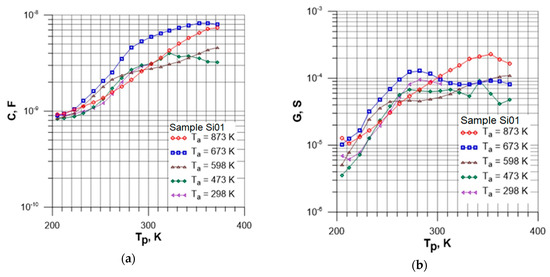
Figure 3.
The temperature dependence of the capacitance (a) and conductance (b) of boron-doped silicon with the substrate resistivity of ρ = 10 Ωcm, implanted with Ne+ ions with a dose of D = 4 × 1013 cm−2 (Sample Si01), recorded for the frequency of the measurement signal f = 10 kHz and different temperatures Ta.
The characteristic G = f(Tp) presented in Figure 3b was made for a Si01 sample doped with boron and having a resistivity of ρ = 10 Ωcm. Taking into account all of the annealing temperatures, the value of the conductance ranges from approximately 3 × 10⁻⁶ S to approximately 2 × 10⁻⁴ S. For the lowest measuring temperatures, the conductance has the highest value for samples annealed at the highest temperatures. Again, the features that indicate the existence of deep energy levels are visible mainly for Ta temperatures of 473 K and 598 K, but also in part for 673 K.
Figure 4a shows the relationship C = f(Tp) for a sample doped with phosphorus with a substrate resistivity of ρ = 10 Ω × cm implanted with Ne+ ions with a dose of D = 4 × 1013 cm−2 recorded for five different annealing temperatures Ta = 298 K, 473 K, 598 K, 673 K, and 873 K.
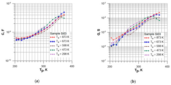
Figure 4.
The temperature dependence of the capacitance (a) and conductance (b) of phosphorus-doped silicon with the substrate resistivity of ρ = 10 Ωcm, implanted with Ne+ ions with a dose of D = 4 × 1013 cm−2 (Sample Si03), recorded for the frequency of the measurement signal f = 10 kHz and different temperatures Ta.
The use of a different element as a dopant for silicon (in this case, phosphorus) can observe some differences for a boron-doped sample of the same resistivity. In the entire measuring temperature range, the capacitance value is slightly lower, for boron it ranges from approximately 5 × 10⁻¹⁰ F to approximately 4 × 10⁻⁹ F, while for phosphorus (the graph above) it is the range from approximately 9 × 10⁻¹⁰ F do ok. 7 × 10⁻⁹ F. Moreover, characteristic inflections indicating the presence of deep energy levels are visible mainly for the annealing temperature Ta = 473 K.
Similar tendencies can be indicated in the conductance curve for the Si03 sample (Figure 4b) with the parameters presented in the description of the capacitance diagram. The characteristic local maxima are visible mainly for the annealing temperature of 473 K. In this case, however, similar tendencies can be noticed at the conductance calculated for the temperature Ta = 598 K. The lack of such features for the highest temperatures indicates that the high-temperature annealing process contributed to a partial or complete disappearance of defects in the silicon crystal structure.
The analysis of the above-mentioned capacitance and conductance courses for all the tested samples showed that the characteristic symptoms, i.e., local maxima in the conductance courses and inflection points in the capacitance courses, occurring in the presence of deep energy levels in the silicon crystal structure, are noticeable primarily for the annealing temperatures Ta = 473 K and Ta = 598 K. Similar trends can be seen in some cases for the annealing temperature of 673 K, but are not so evident. For further analysis of the effect of the type of doping and the dose of implanted neon ions, as well as the calculation of the activation energy, samples subjected to isochronous annealing at the temperature Ta = 598 K were selected.
3.3. The Analysis of the Impact of the Dose of Implanted Ions on Selected Electrical Quantities of the Tested Samples
This subsection presents the dependencies C = f(Tp) and G = f(Tp) made for the sample annealing temperature of 598 K and two measuring frequencies 100 Hz and 100 kHz. Each graph contains runs for two different doses of implanted ions, but for the same dopant of the silicon substrate.
Figure 5a shows the temperature dependence of the capacitance for boron-doped samples (Si01 and Si02) annealed at 598 K with a different dose of implanted neon ions. Both for the dose D = 4 × 1013 cm−2 and D = 4 × 1014 cm−2 characteristic inflections are visible, indicating the existence of deep energy levels. A higher dose of ions causes a slight increase in the capacitance value for measuring temperatures ranging from 220 K to approximately 350 K.
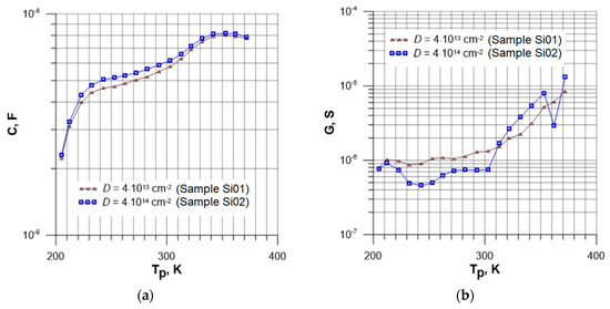
Figure 5.
The dependencies of C = f(Tp) (a) and G = f(Tp) (b) for boron-doped samples, annealed at Ta = 598 K, the frequency of the measurement signal f = 100 Hz and various doses of implanted neon ions (samples Si01 and Si02).
The changes in conductance for boron-doped silicon depending on the measurement temperature for two different ion doses are shown in Figure 5b. The course of the conductance for the lower dose D = 4 × 1013 cm−2 is characterized by smaller fluctuations of values in the entire temperature range. Moreover, for temperatures (203–310) K takes slightly lower values than the course for the higher dose of ions, while above 310 K the situation is the opposite—higher conductance values are achieved for the sample implanted with the dose of D = 4 × 1014 cm−2.
The next characteristics for samples doped with phosphorus were made according to the same principles as the above Figure 5a,b. The temperature dependence of the capacitance shown in Figure 6a shows that, in the case of phosphorus, changing the ion dose by an order of magnitude does not cause significant changes in the capacitance course. Only for lower temperatures a slight deviation of the two runs is visible.
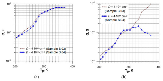
Figure 6.
The dependencies of C = f(Tp) (a) and G = f(Tp) (b) for phosphorus-doped samples, annealed at Ta = 598 K, the frequency of the measurement signal f = 100 Hz and various doses of implanted neon ions (samples Si03 and Si04).
The characteristics of the conductance as a function of the measuring temperature presented in Figure 6b show that for measuring temperatures up to approximately 310 K, the courses are very similar to each other, regardless of the dose of implanted neon ions. The differences appear for temperatures above 310 K, where for the dose D = 4 × 1013 cm−2 an increase in the conductance value is observed, while for the dose D = 4 × 1014 cm−2 a decrease in its value.
Summarizing the above, for samples doped with phosphorus, the change in the dose of the implanted neon ions by an order of magnitude does not significantly affect the capacitance and conductance characteristics. In any case, their shape is very similar to each other and they achieve almost the same values for individual measurement temperatures. In the case of boron-doped silicon, it is visible that, for a larger dose, i.e., D = 4 × 1014 cm−2, higher capacitance and conductance values are assumed for temperatures above 320 K. However, up to this temperature, in most cases, higher values are assumed for the dose D = 4 × 1013 cm−2.
3.4. The Influence of the Type of Dopant on the Change in Capacitance and Conductance of Silicon
The silicon samples on which the tests were carried out also allow the analysis of the obtained results in terms of the influence of the type of dopant on the electrical properties. The following subsection compares the temperature characteristics of the capacitance and conductance for silicon with the same resistivity and the same dose of implanted ions, but with different impurities—for boron and phosphorus. Moreover, the graphs were created for two different values of the frequency of the measurement signal f = 100 Hz and f = 100 kHz.
The capacitance and conductance dependencies shown in Figure 7 were performed as previously for samples with the dose of implanted ions D = 4 × 1013 cm−2, but for the frequency of the measurement signal of f = 100 kHz. Both for the capacitance and conductance runs, higher values are assumed for boron-doped silicon. In the case of the capacitance for boron values in the range (8 × 10⁻¹⁰–3 × 10⁻⁹) F, while for phosphorus (5 × 10⁻¹⁰–2 × 10⁻⁹) F. The conductance characteristics clearly show local maxima, which prove the existence of deep energy levels.
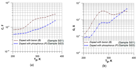
Figure 7.
The temperature dependence of the capacitance (a) and conductance (b) of silicon implanted with neon ions with a dose of D = 4 × 1013 cm−2, annealed at the temperature Ta = 598 K, the frequency of the measurement signal 100 kHz and various impurities (samples Si01 and Si03).
Figure 8 shows the dependencies C = f(Tp) and G = f(Tp) for silicon implanted with neon ions with a dose of D = 4 × 1014 cm−2. As in the previous cases, doping with boron allows to achieve higher capacitance values for the same measurement temperatures as in the case of doping with phosphorus.
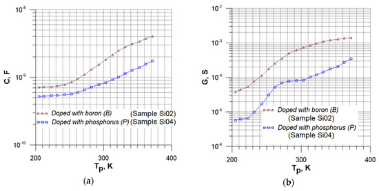
Figure 8.
The temperature dependence of the capacitance (a) and conductance (b) of silicon implanted with neon ions with a dose of D = 4 × 1014 cm−2, annealed at the temperature Ta = 598 K, the frequency of the measurement signal 100 kHz and various impurities (samples Si02 and Si04).
Summarizing the above results, it can be seen on the basis of the graphs that the type of dopant influences the electrical parameters of silicon quite significantly. Doping with boron allows to achieve higher capacitance values in relation to doping with phosphorus, which is visible for both 100 Hz and 100 kHz frequencies. Moreover, especially in the case of courses recorded for a measurement signal with a frequency of 100 Hz, the capacitance varies in a much smaller range of values compared to the phosphorus dopant. Conductance runs for silicon doped with boron, also, in almost all cases, show higher values for specific measurement temperatures.
3.5. The Determination of the Activation Energy of Deep Energy Levels in the Structure of Silicon Implanted with Neon Ions
The next step of the research was to calculate the conduction activation energy ΔE of deep energy levels, the presence of which was found on the basis of the analysis of the temperature courses of the capacitance and conductance dependencies, taking into account the various annealing temperatures described in the previous considerations. The term activation energy was introduced by the Swedish scientist Svante Arrhenius with an equation and law that gives the quantitative basis of the relationship between the activation energy and the rate at which a reaction proceeds [40]. According to the applied methodology [40], one of the methods of determining the activation energy is the approximation of selected parts of the course C = f(1000/Tp) with the function of the equation ln(y) = Ax + B. Figure 9 and Figure 10 show the above-mentioned dependencies C = f(1000/Tp) for two different frequencies f = 100 Hz and f = 100 kHz.
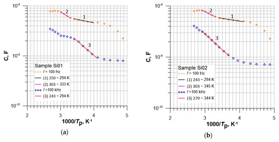
Figure 9.
The dependencies C = f(1000/Tp) for the sample Si01 (a) and Si02 (b), annealed at the temperature Ta = 598 K, registered for the frequency of the measuring signal f = 100 Hz and f = 100 kHz, approximation intervals by the Arrhenius Law, according to the legend.
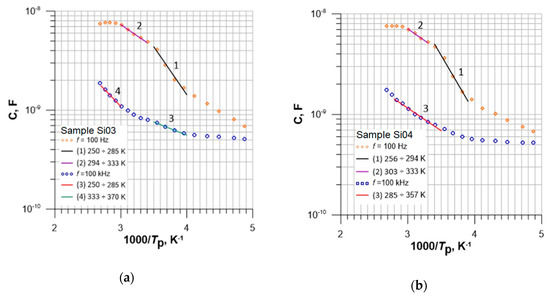
Figure 10.
The dependencies C = f(1000/Tp) for the sample Si03 (a) and Si04 (b), annealed at the temperature Ta = 598 K, registered for the frequency of the measuring signal f = 100 Hz and f = 100 kHz, approximation intervals by the Arrhenius Law, according to the legend.
Then, knowing the form of the approximating curve equation, ΔE was calculated from the relationship:
where: ΔE—conduction activation energy, A—coefficient from the approximating curve equation, k—Boltzmann constant. An Arrhenius plot displays the logarithm of a reaction rate constant, plotted against reciprocal of the temperature. Thanks to the obtained results, the activation energy was determined, which makes it possible to determine the depth of the resulting energy levels.
ΔE = A·1000·k,
The obtained results of the conduction activation energy values are presented in Table 1. The approximation intervals marked with numbers have been precisely characterized in the presented graphs.

Table 1.
The determined values of the activation energy ΔE for conduction for two measuring frequencies f = 100 Hz and f = 100 kHz, for all tested samples with the properties presented in the second chapter.
On the basis of the obtained results, it can be seen that the highest activation energies are achieved for samples of Si03 and Si04 doped with phosphorus, subjected to neon ion implantation with the energy E = 100 keV and the dose of D = 4 × 1013 cm−2 and D = 4 × 1014 cm−2. Moreover, the determined activation energy indicates the depth of the energy levels in relation to the bottom of the conduction band.
4. Conclusions
The conducted research focused on the experimental verification of the possibility of using neon ion implantation to generate radiation defects of the silicon crystal lattice as the base material for photovoltaic cells. The experiment was aimed at determining the influence of the stage and type of silicon defect on its electrical parameters, in terms of the possibility of producing intermediate energy levels in the band gap of a semiconductor, and thus increasing the efficiency of solar cells by enabling a multi-stage transition of electrons from the valence band to the intermediate band, and then to conduction band.
Four monocrystalline silicon samples were selected for the study, differing in the type of dopant (boron and phosphorus) and the size of the dose of implanted neon ions (4 × 1013 cm−2 and 4 × 1014 cm−2). Based on the analysis of empirically determined Arrhenius plots, a number of radiation defects were identified with activation energies ΔE ranging from 0.03 eV to 0.23 eV (Table 1), introducing additional energy levels in the band gap of the tested silicon samples. The conducted research confirmed that the implantation of Ne+ ions enables the production of intermediate energy levels in silicon, and may affect the efficiency of a photovoltaic cell made on its basis.
Based on the results presented in this paper, it is possible to define further research directions related to the use of ion implantation to increase the efficiency of electricity generation in silicon photovoltaic cells. In particular, these activities will be focused on the construction and testing of a prototype of a silicon-based solar cell with a modified band gap structure by neon ion implantation.
Author Contributions
P.W. proposed to study the influence of substrate type and dose of implanted ions on the electrical parameters of silicon in terms of improving the efficiency of photovoltaic cells and guided the work. J.P. and K.D. did the calculations and wrote the paper. P.W. and M.T. revised the results and contributed to the discussions. All authors have read and agreed to the published version of the manuscript.
Funding
This research received no external funding.
Acknowledgments
This work was supported by The National Centre for Research and Development and co-financed from the European Union funds under the Smart Growth Operational Programme (grant # POIR.04.01.04-00-0130/16).
Conflicts of Interest
The authors declare no conflict of interest.
References
- Partyka, J.; Zukowski, P.; Wegierek, P.; Rodzik, A.; Sidorenko, Y.V.; Shostak, Y.A. Temperature dependence of the width of the deep-level band in silicon with a high concentration of defects. Semiconductors 2002, 36, 132–1331. [Google Scholar] [CrossRef]
- Wegierek, P.; Billewicz, P. Changes in the Activation Energy of Radiation Defects in Strongly Defected Silicon Depending on the Type and Concentration of Dopant. Acta Phys. Pol. A 2014, 125, 1392–1395. [Google Scholar] [CrossRef]
- Wegierek, P.; Billewicz, P. Research on Mechanisms of Electric Conduction in the p-Type Silicon Implanted with Ne+ Ions. Acta Phys. Pol. A 2013, 123, 948–951. [Google Scholar] [CrossRef]
- Zinchuk, O.; Drozdov, N.; Fedotov, A.; Mazanik, A.; Krekotsen, N.; Ukhov, V.; Partyka, J.; Wegierek, P.; Koltunowicz, T. Effect of the hydrogen and argon ion-beam treatments on the structural and electrical properties of Cz Si wafers: Comparative study. Vacuum 2009, 83, 99–102. [Google Scholar] [CrossRef]
- Azzouzi, G.; Tazibt, W. Improving silicon solar cell efficiency by using the impurity photovoltaic effect. Energy Procedia 2013, 41, 40–49. [Google Scholar] [CrossRef]
- Małkowski, R.; Jaskólski, M.; Pawlicki, W. Operation of the Hybrid Photovoltaic-Battery System on the Electricity Market—Simulation, Real-Time Tests and Cost Analysis. Energies 2020, 13, 1402. [Google Scholar] [CrossRef]
- Klugmann-Radziemska, E. Shading, Dusting and Incorrect Positioning of Photovoltaic Modules as Important Factors in Performance Reduction. Energies 2020, 13, 1992. [Google Scholar] [CrossRef]
- Zdyb, A.; Gulkowski, S. Performance Assessment of Four Different Photovoltaic Technologies in Poland. Energies 2020, 13, 196. [Google Scholar] [CrossRef]
- Ushasree, P.M.; Bora, B. CHAPTER 1: Silicon Solar Cells, Sol. Energy Capture Mater. 2019, 1–55. [Google Scholar] [CrossRef]
- Saga, T. Advances in crystalline silicon solar cell technology for industrial mass production. NPG Asia Mater. 2010, 2, 96–102. [Google Scholar] [CrossRef]
- Vaderobli, A.; Parikh, D.; Diwekar, U. Optimization under Uncertainty to Reduce the Cost of Energy for Parabolic Trough Solar Power Plants for Different Weather Conditions. Energies 2020, 13, 3131. [Google Scholar] [CrossRef]
- Kowalski, M.; Partyka, J.; Wegierek, P.; Zukowski, P.; Komarov, F.F.; Jurchenko, A.V.; Freik, D. Frequency-dependent annealing characteristics of the implant-isolated GaAs layers. Vacuum 2005, 78, 311–317. [Google Scholar] [CrossRef]
- Wegierek, P.; Billewicz, P. Jump Mechanism of Electric Conduction in n-Type Silicon Implanted with Ne++ Neon Ions. Acta Phys. Pol. A 2011, 120, 122–124. [Google Scholar] [CrossRef]
- Zukowski, P.; Wegierek, P.; Billewicz, P.; Koltunowicz, T.N.; Komarov, F. Jump Mechanism of Electric Charge Transfer in Gallium Arsenide Exposed to Polyenergy Implantation with H+ Ions. Acta Phys. Pol. A 2011, 120, 125–128. [Google Scholar] [CrossRef]
- Green, M.A.; Hishikawa, Y.; Dunlop, E.D.; Levi, D.H.; Hohl-Ebinger, J.; Ho-Baillie, A.W.Y. Solar cel efficiency tables. Prog. Photovolt. Res. Appl. 2018, 26, 3–12. [Google Scholar] [CrossRef]
- NREL’s Best Research-Cell Efficiency Chart. 2020. Available online: https://www.nrel.gov/pv/assets/pdfs/best-research-cell-efficiencies.20200406.pdf (accessed on 2 December 2020).
- Liu, J.; Yao, Y.; Xiao, S.; Gu, X. Review of status developments of high-efficiency crystalline silicon solar cells. J. Phys. D Appl. Phys. 2018, 51, 123001. [Google Scholar] [CrossRef]
- Kozinetz, A.V.; Skryshevsky, V.A. Amorphous submicron layer in depletion region: New approach to increase the silicon solar cell efficiency. Ukr. J. Phys. 2018, 63, 38–48. [Google Scholar] [CrossRef]
- Pavel, A.A.; Khan, M.R.; Islam, N.E. On the possibility of improving silicon solar cell efficiency through impurity photovoltaic effect and compensation. Solid-State Electron. 2010, 54, 1278–1283. [Google Scholar] [CrossRef]
- Węgierek, P.; Pietraszek, J. Application of poly-energy implantation with H + ions for additional energy levels formation in GaAs dedicated to photovoltaic cells. Arch. Electr. Eng. 2019, 68, 925–931. [Google Scholar] [CrossRef]
- Węgierek, P.; Pietraszek, J. Analysis of the Influence of Annealing Temperature on Mechanisms of Charge Carrier Transfer in GaAs in the Aspect of Possible Applications in Photovoltaics. Acta Phys. Pol. A 2019, 136, 299–302. [Google Scholar] [CrossRef]
- Węgierek, P.; Pietraszek, J. Analysis of electricity generation efficiency in photovoltaic building systems made of HIT-IBC cells for multi-family residential buildings. Open Phys. 2019, 17, 307–312. [Google Scholar] [CrossRef]
- Węgierek, P.; Billewicz, P.; Pietraszek, J. Analysis of the influence of ambient conditions on efficiency of HIT-IBC-based photovoltaic system dedicated for energy efficient buildings. In Proceedings of the 2017 International Conference on Electromagnetic Devices and Processes in Environment Protection with Seminar Applications of Superconductors (ELMECO & AoS), Lublin, Poland, 3–6 December 2017. [Google Scholar] [CrossRef]
- Pizzini, S. Towards solar grade silicon: Challenges and benefits for low cost photovoltaics. Sol. Energy Mater. Sol. Cells 2010, 94, 1528–1533. [Google Scholar] [CrossRef]
- Khelifi, S.; Burgelman, M.; Verschraegen, J.; Belghachi, A. Impurity photovoltaic effect in GaAs solar cell with two deep impurity levels. Sol. Energy Mater. Sol. Cells 2008, 92, 1559–1565. [Google Scholar] [CrossRef]
- Irvine, S. Solar Cells and Photovoltaics. In Springer Handbook of Electronic and Photonic Materials; Kasap, S., Capper, P., Eds.; Springer: Cham, Switzerland, 2017; pp. 1097–1109. [Google Scholar] [CrossRef]
- López, E.; Martí, A.; Antolín, E.; Luque, A. On the Potential of Silicon Intermediate Band Solar Cells. Energies 2020, 13, 3044. [Google Scholar] [CrossRef]
- Perez, E.; Duenas, S.; Castan, H.; Garcia, H.; Bailon, L.; Montero, D.; Garcia-Hernansanz, R.; Garcia-Hemme, E.; Olea, J.; Gonzales-Diaz, G. A detailed analysis of the energy levels configuration existing in the band gap of supersaturated silicon with titanium for photovoltaics applications. J. Appl. Phys. 2015, 118, 1–9. [Google Scholar] [CrossRef]
- Okada, Y.; Ekins-Daukes, N.J.; Kita, T.; Tamaki, R.; Yoshida, M.; Pusch, A.; Hess, O.; Phillips, C.C.; Farrell, D.J.; Yoshida, K.; et al. Intermediate band solar cells: Recent progress and future directions. Appl. Phys. Rev. 2015, 2, 1–48. [Google Scholar] [CrossRef]
- Perez, E.; Duenas, S.; Castan, H.; Garcia, H.; Bailon, L.; Montero, D.; Garcia Hernansanz, R.; Garcia, H.E.; Olea, J.; Gonzales-Diaz, G. Energy levels distribution in supersaturated silicon with titanium for photovoltaic applications. Appl. Phys. Lett. 2015, 106, 1–4. [Google Scholar] [CrossRef]
- Billewicz, P.; Wegierek, P.; Grudniewski, T.; Turek, M. Application of Ion Implantation for Intermediate Energy Levels Formation in the Silicon-Based Structures Dedicated for Photovoltaic Purposes. Acta Phys. Pol. A 2017, 132, 274–277. [Google Scholar] [CrossRef]
- Partyka, J.; Wegierek, P.; Zukowski, P.; Sidorenko, Y.; Szostak, Y. Dielectric properties of implanted silicon layers: Influence of rapid thermal annealing. Nucl. Instrum. Methods Phys. Res. Sect. B 2002, 197, 60–66. [Google Scholar] [CrossRef]
- Park, C.; Shim, G.; Balaji, N.; Park, J.; Yi, J. Correlation between Boron–Silicon Bonding Coordination, Oxygen Complexes and Electrical Properties for n-Type c-Si Solar Cell Applications. Energies 2020, 13, 3057. [Google Scholar] [CrossRef]
- Lee, S.; Pham, D.P.; Kim, Y.; Cho, E.C.; Park, J.; Yi, J. Influence of the Carrier Selective Front Contact Layer and Defect State of a-Si: H/c-Si Interface on the Rear Emitter Silicon Heterojunction Solar Cells. Energies 2020, 13, 2948. [Google Scholar] [CrossRef]
- Hieslmair, H.; Mandrell, L.; Latchford, I.; Chun, M.; Sullivan, J.; Adibi, B. High throughput ion-implantation for silicon solar cells. Energy Procedia 2012, 27, 122–128. [Google Scholar] [CrossRef]
- Jeon, M.; Lee, J.; Kim, S.; Lee, W.; Cho, E. Ion implanted crystalline silicon solar cells with blanket and selective emitter. Mater. Sci. Eng. B 2011, 176, 1285–1290. [Google Scholar] [CrossRef]
- Yang, G.; Ingenito, A.; van Hameren, N.; Isabella, O.; Zeman, M. IBC c-Si solar cells based on ion-implanted poly-silicon passivating contacts. Sol. Energy Mater. Sol. Cells 2016, 158, 84–90. [Google Scholar] [CrossRef]
- Billewicz, P. Wykorzystanie Implantacji Jonowej do Zwiększenia Efektywności Wytwarzania Energii Elektrycznej w Ogniwach Fotowoltaicznych Wykonanych na Bazie Krzemu; Politechnika Lubelska: Lublin, Poland, 2018; pp. 1–191. [Google Scholar]
- Iftiquar, S.M.; Lee, Y.; Ju, M.; Balaji, N.; Dhungel, S.K.; Yi, J. Fabrication of Crystalline Silicon Solar Cell with Emitter Diffusion, SiNx Surface Passivation and Screen Printing of Electrode. Photodiodes Fundam. Appl. 2012, 105–131. [Google Scholar] [CrossRef]
- Węgierek, P. Przewodnictwo Elektryczne w Silnie Zdefektowanych Półprzewodnikach Modyfikowanych Technikami Jonowymi; Politechnika Lubelska: Lublin, Poland, 2013; pp. 1–178. [Google Scholar]
- Billewicz, P.; Węgierek, P. Laboratory Stand for Examining the Influence of Environmental Conditions on Electrical Parameters of Photovoltaic Cells. Przegląd Elektrotechniczny 2016, 92, 176–179. [Google Scholar] [CrossRef][Green Version]


Publisher’s Note: MDPI stays neutral with regard to jurisdictional claims in published maps and institutional affiliations. |
© 2020 by the authors. Licensee MDPI, Basel, Switzerland. This article is an open access article distributed under the terms and conditions of the Creative Commons Attribution (CC BY) license (http://creativecommons.org/licenses/by/4.0/).