Abstract
In this study, a novel 4H-SiC double-trench metal-oxide semiconductor field-effect transistor (MOSFET) with a side wall heterojunction diode is proposed and investigated by conducting numerical technology computer-aided design simulations. The junction between P+ polysilicon and the N-drift layer forming a heterojunction diode on the side wall of the source trench region suppresses the operation of the PiN body diode during the reverse conduction state. Therefore, the injected minority carriers are completely suppressed, reducing the reverse recovery current by 73%, compared to the PiN body diodes. The switching characteristics of the proposed MOSFET using the heterojunction diode as a freewheeling diode was compared to the power module with a conventional MOSFET and an external diode as a freewheeling diode. It is shown that the switching performance of the proposed structure exhibits equivalent characteristics compared to the power module, enabling the elimination of an external freewheeling diode in the power system.
1. Introduction
Silicon carbide (SiC), a wide-bandgap semiconductor, is considered a promising material for the next-generation power system [1,2,3,4]. It has a critical electric field of 3 MV/cm, which is ten times higher than that of silicon [5]. Therefore, the resistance of an extremely low drift region can be achieved for high voltage applications. In addition, the thermal conductivity of SiC is three times greater than that of silicon, which suppresses catastrophic failure during the high temperature operation of a device.
Among various SiC-based devices, as shown in Figure 1a, a 4H-SiC UMOSFET was preferred to provide a better tradeoff between breakdown voltage and on-resistance (Ron) than a planar VDMOSFET [6,7,8,9]. However, a UMOSFET has the disadvantage of a strong electric field in the bottom region of the gate, causing premature breakdown and oxide reliability problems. Recently, a double-trench UMOSFET (DT-UMOSFET) structure, shown in Figure 1b, has been developed to distribute the electric field concentrated on gate oxide to the deep p-type doping of the source region [10,11,12]. Thus, the DT-UMOSFET has better static performance than a conventional UMOSFET (C-UMOSFET). Consequently, the manufacturers are gradually adopting DT-UMOSFETs when using a power system.
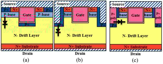
Figure 1.
Schematic cross-sectional views of (a) C-UMOSFET, (b) DT-UMOSFET, and (c) DT-HJDUMOSFET.
In the power inverter and converter system, an external anti-parallel Schottky barrier diode (SBD) is widely used as a freewheeling diode [13,14,15]. To reduce the chip size of the module and parasitic components such as stray inductance, many efforts have been made to use the parasitic PiN body diode of a MOSFET as a freewheeling diode. However, there are some problems when using the PiN body diode of a SiC MOSFET. Because the parasitic PiN body diode is a bipolar device, unlike an SBD, it has a much larger reverse recovery current and a higher turn-on voltage drop. Consequently, it causes the device to increase the overall switching loss of the system [16]. In addition, when the PiN body diode is conducted, a bipolar degradation effect may occur in which the parasitic NPN transistor is switched on [17,18]. Many approaches have been proposed to eliminate the issues mentioned above. The method of carrier lifetime control was adopted to reduce the concentration of minority carriers. However, this method can increase resistance in the drift region and cause metallization contamination [19]. Moreover, Schottky diodes can be integrated directly into the MOSFET; however, this increases the leakage current due to the image charge of the metal–semiconductor junction, and requires an additional cell pitch that reduces the specific on-resistance [20,21]. Contamination by metal for Schottky contact can also occur.
In this paper, a novel DT-UMOSFET with a self-aligned sidewall heterojunction diode (DT-HJDUMOSFET) is proposed to solve the above-mentioned problem efficiently. The heterojunction diode (HJD) made of polysilicon and 4H-SiC behaves like an SBD due to unipolar action in reverse conduction [22]. Thus, the proposed device features some excellent body diode characteristics, such as reverse recovery and turn-on voltage, and eliminates the bipolar degradation effect. The HJD is integrated into the proposed device, eliminating the need for an additional anti-parallel SBD in the power inverter and converter systems. Hence, the proposed structure minimizes additional fabrication process steps; in particular, no photo-lithography mask is added.
2. Device Structure and Features
Figure 1c shows the schematic cross-sectional view of the proposed DT-HJDUMOSFET structure. Like a DT-UMOSFET, the source trench P+ shielding region of the DT-HJDUMOSFET disperses the electric field concentrated on the gate oxide to mitigate electric field crowding. Accordingly, the breakdown voltage of the DT-HJDUMOSFET can be increased compared to the C-UMOSFET. The main difference is the structure of the body diode. Compared to the DT-UMOSFET, the source trench region of the DT-HJDUMOSFET is deposited by P+ polysilicon. The HJD between the P+ polysilicon and N-drift region acts like an SBD, and the PiN diode is suppressed due to the low turn-on voltage of the HJD.
All structures have the same thickness and doping concentration of 16 μm and 3 × 1015 cm−3, respectively, for a rated breakdown voltage of 1700 V. The length and doping concentration of the channel are 0.7 μm and 1 × 1017 cm−3, respectively. The width and depth of the gate trench are 2.0 μm and 1.8 μm, respectively. The thickness of the gate oxide layer is 50 nm based on process limitation. The DT-UMOSFET and DT-HJDUMOSFET structures have the same width and depth of the source trench; these are 1.0 μm and 1.8 μm, respectively, to proceed simultaneously with the gate trench process.
Figure 2 shows the feasible self-aligned fabrication process steps of the DT-HJDUMOSFET by using TCAD process simulation. The doping concentration in Figure 2 is calculated only with activated impurities. After the formation of source, base and P+ shielding regions using ion implantation, the source trench process is carried out to make the HJD region. The gate is formed by carrying out thermal oxidation and polysilicon deposition. In addition, P+ polysilicon is deposited to create a heterojunction between P+ polysilicon and the N-drift layer. This means that the self-aligned process that does not require an additional mask is introduced to compose HJD. Lastly, the metallization process is carried out to connect the source electrode. The photoresist has been omitted in Figure 2.
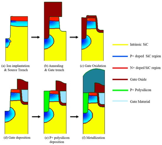
Figure 2.
Proposed fabrication procedure of DT-HJDUMOSFET. (a) Forming source, base and P+ shielding region through ion implantation and source trench region, (b) annealing and trench gate region, (c) gate oxidation, (d) gate polysilicon deposition, (e) P+ polysilicon deposition to create heterojunction diode (HJD), (f) Metallization.
The energy band diagram of the body diode region of the DT-HJDUMOSFET is shown in Figure 3 to explain its body diode operation. Figure 3a shows the schematic view of diode portion in the DT-HJDUMOSFET. The gate and oxide regions are omitted in Figure 3a. There are two diode structures, PiN diode and HJD, along the lines of A-A’ and B-B’, respectively. As shown in Figure 3b,d, when the source-drain voltage is 0 V, there is a potential barrier height of electrons (ϕBn) at 2.1 eV and 1.6 eV, respectively. Thus, the transport of the electrons and holes are prohibited due to the formation of a high potential barrier. When the source-drain voltage is 2 V, the energy band of the PiN diode part is shown in Figure 3c. There is still ϕBn at 0.8 eV along the PN junction. Thus, no electron movement is generated to produce current.
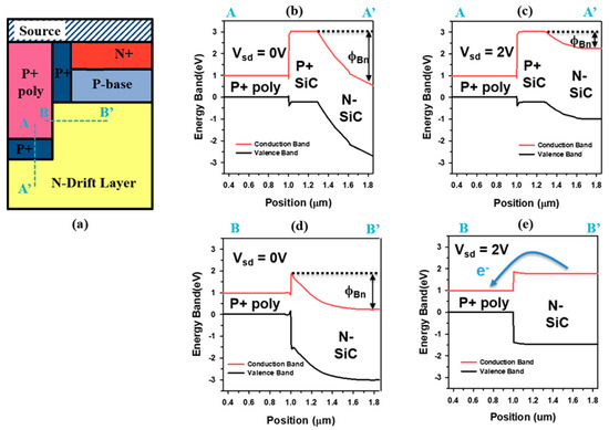
Figure 3.
(a) Schematic cross-sectional view of DT-HJDUMOSFET’s body diode region. Band diagram along A-A’ line with (b) Vsd = 0 V and (c) Vsd = 2 V, and along B-B’ line with (d) Vsd = 0 V and (e) Vsd = 2 V, respectively.
The differences in HJD compared to PiN diodes under the same conditions are shown in Figure 3e. The transfer of electrons is allowed from N-SiC to P+ polysilicon on the conduction band due to lowered ϕBn. However, holes still face a high barrier height when moving to the N-SiC region. Therefore, only the electronic current consists of the body diode current and it acts as a unipolar device. This feature influences the characteristics of the device’s body diode.
3. Results and Discussion
In this section, the results of the numerical simulations of three devices, shown in Figure 1, are presented to evaluate electrical characteristics. The characteristics of the devices were analyzed using the two-dimensional and mixed-mode technology computer-aided design (TCAD) simulation tool. The simulation includes the temperature-dependent Shockley–Read–Hall and Auger recombination. The mobility model includes doping-dependent, high-field saturation, and mobility degradation. In addition, anisotropic and incomplete impact ionization effects were considered in this model. TCAD simulation was performed through 2D finite element analysis (FEA) methodology.
3.1. Static Characteristics
Figure 4 shows the static characteristics such as breakdown voltage, on-resistance, and leakage current of the three devices. The forward conduction characteristics are obtained at Vgs = 15 V. The on-resistance is compared when the breakdown voltage of each structure is designed to be 1700 V by optimizing the thickness and doping concentration of the epi-layer of each structure. Because there is no JFET resistance between the trench bottom P+ shielding and base region, the DT-UMOSFET and DT-HJDUMOSFET have lower Ron (5.67 mΩcm2) than the C-UMOSFET (16.55 mΩcm2). In addition, the leakage current levels of the DT-UMOSFET and DT-UMOSFET are slightly higher than that of the C-UMOSFET owing to the increased PN junction area. However, this difference is very small and can be neglected.
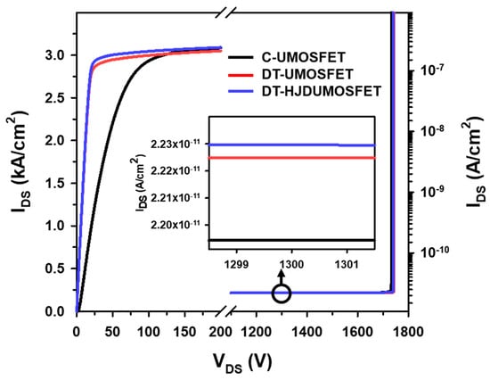
Figure 4.
Static characteristics as forward conduction characteristics, breakdown voltages, and leakage current levels of C-UMOSFET, DT-UMOSFET, and DT-HJDUMOSFET.
Figure 5 shows the electric field distribution of the DT-HJDUMOSFET at Vds = 1200 V. Because the critical electric field of silicon is ten times smaller than that of SiC, a large electric field should not be applied to the polysilicon region. As shown in Figure 5, the electric field crowding is clearly visible around the corner of the P+ shielding region. Thus, the P+ shielding region efficiently blocks the electric field applied to the polysilicon sides. Furthermore, the electric field in oxide should not exceed the safety limit (4 MV/cm [23]) at Vds = 1200 V. The excess of safety limit affects the long-time reliability of the device, causing problems such as premature breakdown or hot carrier injection [24]. As shown in Figure 5, the density of the electric field at the gate oxide is less than 4 MV/cm owing to the dispersed field by P+ shielding at the source trench region. In particular, the DT-HJDUMOSFET is the device structure that has superior reliability with respect to high electric field distribution.
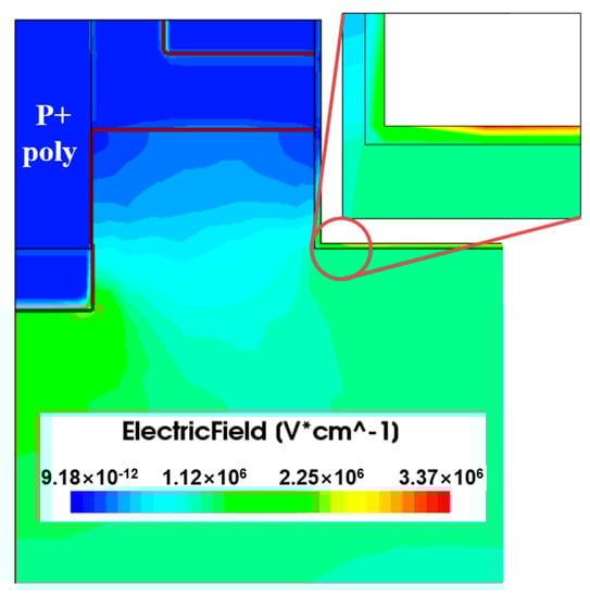
Figure 5.
Electric field distribution of DT-HJDUMOSFET at Vds = 1200 V. The magnified area is the bottom gate oxide.
3.2. Body Diode Characteristics
As the DT-HJDUMOSFET is used as a freewheeling diode, its body diode characteristics that can affect its properties of dynamic operation should be considered. The minority carrier lifetime of each device is 1.2 µs by default, and various models related to carrier lifetime are applied. In Figure 6, the density distributions of the minority carriers (holes) of the DT-UMOSFET and DT-HJDUMOSFET are shown. Unlike the DT-UMOSFET, the body diode of the DT-HJDUMOSFET acts like a unipolar device, as shown in the band diagram of Figure 2e. Therefore, the HJD is effective in suppressing minority carrier injection into the drift region. This feature improves characteristics such as thermal stability or reverse recovery of its body diode.
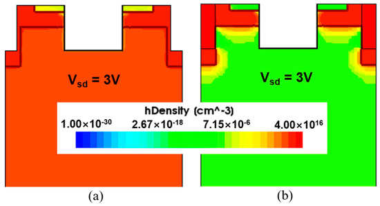
Figure 6.
Density distributions of minority carriers (holes) at Vsd = 3 V of (a) DT-UMOSFET and (b) DT-HJDUMOSFET.
Figure 7 shows the reverse recovery current waveforms of the DT-UMOSFET and DT-HJDUMOSFET when load current is 100 A/cm2. In the DT-UMOSFET, the total reverse recovery charge (Qrr, 2419 nC/cm2) is made up of injection current as the time derivative of the charge of injected carriers and junction current due to the discharge of junction capacitance. Therefore, the reverse recovery current (Irr) is expressed as follows [25]:
where Qinj is the charge of injected minority carriers, and Qj is the charge of ionized dopant atoms stored in the voltage-dependent junction capacitance.
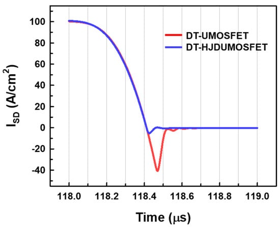
Figure 7.
Reverse recovery current waveform of the body diode for DT-UMOSFET and DT-HJDUMOSFET.
In the case of DT-HJDUMOSFET, the total reverse recovery charge (649 nC/cm2) is significantly reduced by 73% due to the suppressed injection of minority carriers, as shown in Figure 6b. The total current consists of only the junction current from the discharging junction capacitance. The improved reverse recovery characteristics contribute to better dynamic switching loss in the power system.
In Figure 8, the forward conduction characteristics of the body diode are shown according to variations in the temperature of both structures. As shown in Figure 8, the DT-HJDUMOSFET has a lower turn-on voltage than the DT-UMOSFET. In HJD, the on-state voltage drop (VF), including the resistive voltage drop, is expressed as follows:
where JF is the forward current density, JS is the reverse saturation current density, RS is the total series-specific resistance, k is the Boltzmann constant, and T is the thermodynamic temperature. JS is derived as follows [26]:
where A is the Richardson’s constant, and ϕb is the barrier height of the junction between SiC and polysilicon.
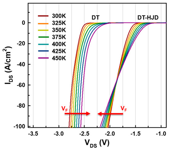
Figure 8.
Forward conduction characteristics of the body diode of DT-UMOSFET and DT-HJDUMOSFET in temperature range of 300 K to 450 K.
At a low current level, the voltage drop is associated with the barrier being reduced by the rise in temperature. On the contrary, at a high current level, the resistance of the drift region increases with the rise in temperature, owing to the degradation of electron mobility, and consequently, the on-state voltage drop increases. For the nominal operating current density of 100 A/cm2, the on-state voltage drop has a positive temperature coefficient, indicating a stable operation of the freewheeling diode.
Furthermore, when the body diode is switched on, the bipolar degradation effect may occur due to a voltage drop across the N+ source and p-base region. However, in the case of DT-HJDUMOSFET, the bipolar degradation effect is suppressed because there is no current flow into the p-base region. Therefore, it is free from the bipolar degradation that is commonly encountered when the body diode is actively used. Thus, we can eliminate an external freewheeling diode, such as an SBD. The comprehensive characteristics of the body diodes of the DT-UMOSFET and DT-HJDUMOSFET are shown in Table 1.

Table 1.
Comparison of body diode characteristics.
3.3. Switching Characteristics
In this section, the switching characteristics of the devices are discussed in detail. Figure 9 shows the simulation test circuits for evaluating the switching performance of the devices. The double pulse test circuit is used to test switching characteristics [27]. We analyzed the waveform of the lower-side MOSFET. Instead of using a freewheeling diode such as an SBD, we use the MOSFET as the same type of bottom device. We simulate a single unit, as shown in Figure 9a,c, and a power module combining the DT-UMOSFET and SBD, as shown in Figure 9b. The load inductor is used to replicate circuit conditions in the converter design. The cell area of all devices under test is set to 1.0 cm2. The gate resistance Rg is set to 1Ω, and the gate turn on-off voltages are 15 V and −5 V, respectively. The load inductance Ld is set to 400 μH, and VDD is 800 V.
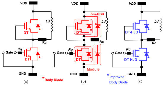
Figure 9.
Equivalent test circuit configuration for switching characteristics of (a) DT-UMOSFET, (b) power module composed of DT-UMOSFET and SBD, and (c) DT-HJDUMOSFET.
The switching curves of three cases are shown in Figure 10 and Figure 11. The comprehensive switching characteristics are shown in Table 2. The energy losses during the switching transition is expressed as follows [16]:
where t is the switching time delay, Eon and Eoff are the energy losses at turn-on and turn-off transient, respectively. The time delay is required to charge and discharge the capacitance of the devices until the gate voltage reaches the Miller plateau value. In the DT-HJDUMOSFET, the integrated HJD does not affect the charge or capacitance of the gate of the device compared to the DT-UMOSFET, and the switching time does not differ in the three cases. Therefore, the energy losses of the devices in the three cases are mainly affected by IDS.
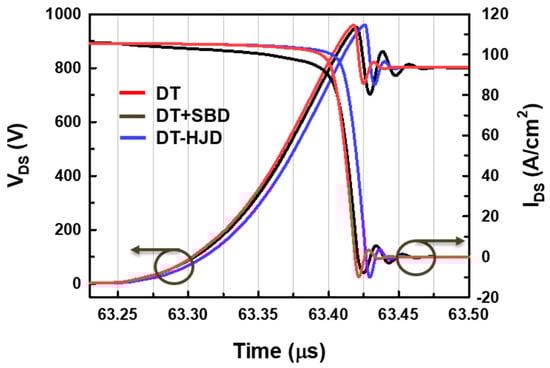
Figure 10.
Turn-off curves of DT-UMOSFET, power module composed of DT-UMOSFET and SBD, and DT-HJDUMOSFET.
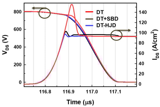
Figure 11.
Turn-off curves of DT-UMOSFET, power module composed of DT-UMOSFET and SBD, and DT-HJDUMOSFET.
Table 2.
Comparison of switching characteristics.
In the turn-off waveform, the upper-side device, acting as a freewheeling diode, is switched to the forward conduction state. Therefore, there is no current overshoot owing to the reverse recovery charge of the freewheeling diode from the upper-side device, as shown in Figure 10. Therefore, the differences in Eoff of the three cases are negligible.
By contrast, in the turn-on waveform, the reverse recovery current from the upper-side device affects the switching characteristics of the lower MOSFET, as shown in Figure 11. This increases the current overshoot of the DT-UMOSFET to a great extent. Therefore, the DT-UMOSFET shows a significant increase in energy loss owing to current overshoot. In our test circuits, the peak current level in turn-on transient (Ipeak) of 148.9 A/cm2 and Eon of 0.467 mJ/cm2 are obtained. As shown in Figure 9b, this problem can be addressed by arranging the freewheeling diode, such as the SBD, in parallel, as before. In the power module, current overshoot is suppressed due to the lower reverse recovery current of SBD. As a result, Ipeak (102.4 A/cm2) and Eon (0.376 mJ/cm2) are significantly improved.
Meanwhile, the DT-HJDUMOSFET that is not combined with an anti-parallel freewheeling diode does not have high current overshoot because its body diode has a low reverse recovery charge like SBD. In addition, the slightly improved levels of Ipeak (96.8 A/cm2) and Eon (0.361 mJ/cm2) are obtained against the power module despite the reduced number of devices in the test circuit, as shown in Figure 9. Compared to the power module, the usage of DT-HJDUMOSFET has an advantage in the removal of parasitic components, such as stray inductance, while achieving an improved performance. Therefore, the DT-HJDUMOSFET structure can play a critical role in the development of advanced power device technology.
4. Conclusions
A novel 4H-SiC double-trench MOSFET with side wall heterojunction diode (DT-HJDUMOSFET) is proposed, and its advantages are analyzed and verified by conducting numerical TCAD simulations. Compared to the DT-UMOSFET, the proposed DT-HJDUMOSFET exhibits a similar specific Ron of 5.67 mΩcm2, breakdown voltage of 1700 V, and does not have a reliability problem with respect to high electric field distribution. Due to the unipolar action of HJD like an SBD, the DT-HJDUMOSFET exhibits a reverse recovery charge that was significantly reduced by 73%, including a positive temperature coefficient of forward voltage drop, compared to the DT-UMOSFET. As a result, the DT-HJDUMOSFET shows enhanced switching characteristics, such that Eon and Ipeak are decreased by factors of ~1.29 and ~1.54, respectively. In addition, compared to the power module configured in parallel with the DT-UMOSFET and SBD, the proposed structure does not degrade the switching performance of the device. Therefore, when we design a power converter circuit, the proposed device structure can reduce the chip size by eliminating the freewheeling diode and remove the parasitic component without performance degradation.
Author Contributions
All authors contributed to this work. Investigation, J.K., K.K.; Methodology, J.K., K.K.; Supervision, J.K., K.K.; Writing-original draft, J.K.; Writing-review and editing, K.K. All authors have read and agreed to the published version of the manuscript.
Funding
This research received no external funding.
Acknowledgments
This research is supported by the MIST (Ministry of Science and ICT), Korea, under the ITRC (Information Technology Research Center) support program (IITP-2020-2018-0-01421) supervised by the IITP (Institute for Information & Communications Technology Planning & Evaluation).
Conflicts of Interest
The authors declare no conflict of interest.
References
- Zeng, Z.; Li, X. Comparative study on multiple degrees of freedom of gate drivers for transient behavior regulation of SiC MOSFET. IEEE Trans. Power Electron. 2018, 33, 8754–8763. [Google Scholar] [CrossRef]
- Jin, M.; Gao, Q.; Wang, Y.; Xu, D. A temperature-dependent SiC MOSFET modeling method based on MATLAB/Simulink. IEEE Access 2018, 6, 4497–4505. [Google Scholar] [CrossRef]
- Zhang, J.; Wu, H.; Zhao, J.; Zhang, Y.; Zhu, Y. A resonant gate driver for silicon carbide MOSFETs. IEEE Access 2018, 6, 78394–78401. [Google Scholar] [CrossRef]
- Wang, J.; Zhao, T.; Li, J.; Huang, A.Q.; Callanan, R.; Husna, F.; Agarwal, A. Characterization, modeling, and application of 10-kV SiC MOSFET. IEEE Trans. Electron Devices 2008, 55, 1798–1806. [Google Scholar] [CrossRef]
- Kimoto, T. Ultrahigh-voltage SiC devices for future power infrastructure. In Proceedings of the 2013 Proceedings of the European Solid-State Device Research Conference (ESSDERC), Bucharest, Romania, 16–20 September 2013; pp. 22–29. [Google Scholar]
- Uchida, K.; Saitoh, Y.; Hiyoshi, T.; Masuda, T.; Wada, K.; Tamaso, H.; Hatayama, T.; Hiratsuka, K.; Tsuno, T.; Furumai, M.; et al. The optimised design and characterization of 1200 V/2.0 mΩ cm2 4H-SiC V-groove trench MOSFETs. In Proceedings of the IEEE 27th International Symposium on Power Semiconductor Devices IC’s (ISPSD), Hong Kong, China, 10–14 May 2015; pp. 85–88. [Google Scholar]
- Qingwen, S.; Xiaoyan, T.; Yimeng, Z.; Yuming, Z.; Yimen, Z. Investigation of SiC trench MOSFET with floating islands. IET Power Electron. 2016, 9, 2492–2499. [Google Scholar] [CrossRef]
- Bharti, D.; Islam, A. Optimization of SiC UMOSFET structure for improvement of breakdown voltage and ON-resistance. IEEE Trans. Electron Devices 2018, 65, 615–621. [Google Scholar] [CrossRef]
- Tan, J.; Cooper, J.A.; Melloch, M.R. High-voltage accumulationlayer UMOSFET’s in 4H-SiC. IEEE Electron Device Lett. 1998, 19, 487–489. [Google Scholar] [CrossRef]
- Nakamura, T.; Nakano, Y.; Aketa, M.; Nakamura, R.; Mitani, S.; Sakairi, H.; Yokotsuji, Y. High performance SiC trench devices with ultra-low ron. In Proceedings of the 2011 International Device Meeting, Washington, DC, USA, 5–7 December 2011. [Google Scholar]
- Wei, J.; Liu, S.; Yang, L.; Tang, L.; Lou, R.; Li, T.; Fang, J.; Li, S.; Zhang, C.; Sun, W. Investigations on the degradations of double-trench SiC power MOSFETs under repetitive avalanche stress. IEEE Trans. Electron Devices 2019, 66, 546–552. [Google Scholar] [CrossRef]
- Sampath, M.; Morisette, D.T.; Cooper, J.A. Comparison of Single- and Double-Trench UMOSFETs in 4H-SiC. Mater. Sci. Forum 2018, 924, 752. [Google Scholar] [CrossRef]
- Jiang, H.; Wei, J.; Dai, X.; Zheng, C.; Ke, M.; Deng, X.; Sharma, Y.; Deviny, I.; Mawby, P. SiC MOSFET with built-in SBD for reduction of reverse recovery charge and switching loss in 10-kV applications. In Proceedings of the ISPSD, Sapporo, Japan, 28 May–1 June 2017; pp. 49–52. [Google Scholar]
- Conrad, M.; DeDoncker, R.W. Avoiding reverse recovery effects in super junction MOSFET based half-bridges. In Proceedings of the IEEE International Symposium on Power Electronics for Distributed Generation Systems, Aachen, Germany, 22–25 June 2015; pp. 1–5. [Google Scholar]
- Yamashita, N.; Murakami, N.; Yachi, T. Conduction power loss in MOSFET synchronous rectifier with parallel-connected Schottky barrier diode. IEEE Trans. Power Electron. 1998, 13, 667–673. [Google Scholar] [CrossRef]
- Ren, Y.; Xu, M.; Zhou, J.; Lee, F.C. Analytical loss model of power MOSFET. IEEE Trans. Power Electron. 2006, 21, 310–319. [Google Scholar]
- Ishigaki, T.; Murata, T.; Kinoshita, K.; Morikawa, T.; Oda, T.; Fujita, R.; Konishi, K.; Mori, Y.; Shima, A. Analysis of degradation phenomena in bipolar degradation screening process for SiC-MOSFETs. In Proceedings of the 31st International Symposium on Power Semiconductor Devices and ICs (ISPSD), Shanghai, China, 19–23 May 2019; pp. 259–262. [Google Scholar]
- Ishigaki, T.; Hayakawa, S.; Murata, T.; Masuda, T.; Oda, T.; Takayanagi, Y. Diode-Less SiC Power Module with Countermeasures Against Bipolar Degradation to Achieve Ultrahigh Power Density. IEEE Trans. Electron Devices 2020, 67, 2035–2043. [Google Scholar] [CrossRef]
- Saito, W.; Ono, S.; Yamashita, H. Influence of carrier lifetime control process in superjunction MOSFET characteristics. In Proceedings of the ISPSD, Waikoloa, HI, USA, 15–19 June 2014; pp. 87–90. [Google Scholar]
- Shenai, K.; Baliga, B.J. Monolithically integrated power MOSFET and Schottky diode with improved reverse recovery characteristics. IEEE Trans. Electron Devices 1990, 37, 1167–1169. [Google Scholar] [CrossRef]
- Cheng, X.; Sin, J.K.O.; Kang, B.; Feng, C.; Wu, Y.; Liu, X. Fast reverse recovery body diode in high-voltage VDMOSFET using cell distributed Schottky contacts. IEEE Trans. Electron Devices 2003, 50, 1422–1425. [Google Scholar] [CrossRef]
- Tanaka, H.; Hayashi, T.; Shimoida, Y.; Yamagami, S.; Tanimoto, S.; Hoshi, M. Ultra-low von and high voltage 4H-SiC heterojunction diode. In Proceedings of the IEEE 17th Int. Symp. Power Semiconductor Devices ICs (ISPSD), Santa Barbara, CA, USA, 23–26 May 2005; pp. 287–290. [Google Scholar]
- Zhou, X.; Yue, R.; Zhang, J.; Dai, G.; Li, J.; Wang, Y. 4H-SiC trench MOSFET with floating/grounded junction barrier-controlled gate structure. IEEE Trans. Electron Devices 2017, 64, 4568–4574. [Google Scholar] [CrossRef]
- Zhou, X.; Su, H.; Yue, R.; Dai, G.; Li, J.; Wang, Y.; Yu, Z. A deep insight into the degradation of 1.2-kV 4H-SiC MOSFETs under repetitive unclamped inductive switching stresses. IEEE Trans. Power Electron. 2018, 33, 5251–5261. [Google Scholar] [CrossRef]
- Banáš, S.; Divín, J.; Dobešb, J.; Paňkoa, V. Accurate diode behavior model with reverse recovery. Solid State Electron. 2018, 139, 31–38. [Google Scholar] [CrossRef]
- Wang, Y.; Wang, H.-Y.; Cao, F.; Wang, H.-Y. High performance of polysilicon/4H-SiC dual-heterojunction trench diode. IEEE Trans. Electron Devices 2017, 64, 1653–1659. [Google Scholar] [CrossRef]
- Wei, J.; Zhang, M.; Jiang, H.; Wang, H.; Chen, K.J. Dynamic degradation in SiC trench MOSFET with a floating p-shield revealed with numerical simulations. IEEE Trans. Electron Devices 2017, 64, 2592–2598. [Google Scholar] [CrossRef]
© 2020 by the authors. Licensee MDPI, Basel, Switzerland. This article is an open access article distributed under the terms and conditions of the Creative Commons Attribution (CC BY) license (http://creativecommons.org/licenses/by/4.0/).