Abstract
For over a decade, single-junction perovskite solar cells (PSCs) have experienced an unprecedent increase in efficiencies and even offer opportunities to surpass the Shockley–Queisser limit in multijunction configuration. There is consequently an intense need for easily processable semi-transparent PSCs as a basis of affordable tandems. The current study reports the comparison of negative-intrinsic-positive (NIP) and positive-intrinsic-negative (PIN) architectures based on CH3NH3PbI3{Cl}-based perovskite. Both devices could be prepared with the same N-type (SnO2 nanoparticles) and P-type (poly-triarylamine (PTAA) polymer) materials. Each layer (except for electrodes) was deposited using solvent-based low temperature processes, contrasting with other literature studies, especially SnO2 for PIN-type purposes. A thorough experimental comparison of the two architectures reveals rather similar optical and structural properties for perovskites, whether deposited on an N- or P-type underlayer, with also comparable efficiencies in the final devices. A compatible deposition process for sputtered indium tin oxide (ITO) as a semi-transparent electrode was then performed for both architectures. Upon varying the illuminated devices’ side, the semi-transparent cells exhibited different photocurrent behaviors, the magnitude of which depended on the device’s architecture. In conclusion, despite slightly better efficiencies for the semi-transparent NIP-type devices, the semi-transparent PIN-type counterparts also appear to be optically attractive for (two-terminal) tandem applications.
1. Introduction
ABX3 perovskite materials as absorber layers have facilitated sensational growth in the photovoltaic (PV) performance of solar cells [1]. These materials possess outstanding optoelectronic properties, unexpected from low temperature solution process routes [2]. Their high defect tolerance [3] and indirect bandgap features (almost direct with the Rashba effect [4]), combined with a weak exciton binding energy at room temperature [5], induce low bulk and surface recombination [6,7], long carrier diffusion lengths [8] and bipolar transport with high charge carrier mobilities [9]. Moreover, perovskite materials exhibit high absorption coefficients and low sub-bandgap absorptions [10]. The sharp absorption onset may be varied with the chemistry and processing conditions to tune the perovskite’s bandgap within a wide range from 1.17 to 3.11 eV [11,12,13,14,15]. As a result, perovskite materials have garnered great interest for tandem applications [16,17], especially with silicon cells [18,19,20,21,22], the main goal being to enhance the power conversion efficiency (PCE) even beyond the Shockley–Queisser limit [23].
Perovskite solar cells (PSCs) may be manufactured following two different paths depending on whether the electron transport layer (ETL) or the hole transport layer (HTL) is deposited first. This leads to the so-called “standard architecture” (negative-intrinsic-positive, NIP-type) or “inverted architecture” (positive-intrinsic-negative, PIN-type), respectively (Figure 1a). The former architecture was first proposed in 2009 using titanium oxide (TiO2) as the ETL [24]. A PIN-type device was published four years later in 2013 with the use of poly(3,4-ethylene dioxythiophene) doped with poly(styrene-sulfonate) (PEDOT:PSS) as an organic HTL [25]. Today, both architectures can reach high power conversion efficiencies (PCE) above 20–22% [26,27], but NIP-type PSCs have led to the published record efficiencies for single-junction cells [26,28]. In comparison, typical efficiencies remain significantly lower in PIN-type PSCs using similar perovskites [29]. This difference may result from lower open-circuit voltage (Voc) for PIN-type PSCs due to the non-suitable doping state of the perovskite near its N-type interface leading to a higher non-radiative recombination rate [30]. Very few authors have tried to directly compare NIP- and PIN-type architectures using the same ETL and HTL. Often, different ETLs and HTLs are preferred because they seem more suitable for a given architecture due to their process compatibility or simply because they lead to higher PCE. That PCE race may hinder, to some extent, the role of research by detracting from its fundamental goal to improve knowledge and understanding. The study of C. Momblona et al. is different in this matter; they reported a direct comparison and developed a comprehensive optimization of the two interfacial materials (organic small molecules) for the two kinds of architectures [31]. As a result, they concluded that both architectures lead to high efficiencies with the same elaboration process, particularly for the NIP-type cells due to a higher Voc and fill factor (FF). The observed difference may reside at the P-type interface where hole extraction would be more hindered for the PIN-type architecture.
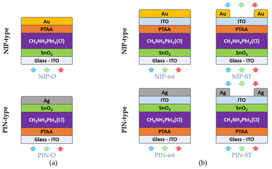
Figure 1.
Illustration of the stacks used in this study for both negative-intrinsic-positive (NIP) and positive-intrinsic-negative (PIN) architectures: (a) reference opaque devices (NIP-O and PIN-O); (b) their respective intermediary opaque (NIP-int and PIN-int) and semi-transparent devices (NIP-ST and PIN-ST).
Despite this tendency, tandem applications combining perovskite and silicon indicate the opposite trend: the highest tandem efficiencies reported in the literature are indeed for PIN-type PCSs [18]. The general explanation for this experimental observation is that PIN-type PSCs allow the reduction of parasitic absorption in the front metal contact, as compared to the standard architecture [20]. The fabrication order and the broad use of a thick HTL with high optical absorption for the P-type contact in the NIP-type architecture appear to be mainly responsible for this [18]. Nonetheless, PIN-type PSCs systematically include fullerene materials as ETLs [32] (because of their good affinity with perovskites as a passivating layer [33]), which are also known to have a large parasitic absorption [18,20]. A thorough optimization of a tandem cell for high efficiency should therefore rely on the minimization of the undesirable absorptions, especially from the illuminated tandem’s side. In other words, there is a need for good control of the optical characteristics of the individual layers and their combination [18,34]. Semi-transparent PSCs have become gradually more studied and published in recent literature [19,21,22,35,36,37,38,39]. The authors reported PCEs between 9 and 17%, depending on the illumination side and the materials used for the transparent conductive layers. This is thus of interest to identify the most promising architecture and understand why the best tandem structures have been reported with the PIN architecture, while the NIP architecture remains preferred in single cell configurations.
The current work focuses on a direct comparison of planar PSCs using the two NIP- and PIN-type architectures in a simple (limitation of the layers) configuration (Figure 1a) for an industrial scope. Single undoped HTL and ETL layers were used, and the latter did not contain any fullerene materials, even in the PIN-type architecture. The PSCs were first elaborated in an opaque configuration. Then, semi-transparent (ST) devices were crafted, to estimate the potential interest for tandem applications. The top transparent electrode was integrated with sputtered ITO (indium tin oxide) to favor normal photon transmission as well as the lateral charge carriers’ transport (Figure 1b). ITO was deposited at room temperature, entirely compatible with the perovskite materials. The quality of the ITO layer and its compatibility depending on the PSC’s architecture was then tested using J–V measurements, as was the influence of the illumination side.
Tin oxide nanoparticles (np-SnO2) and poly-triarylamine polymer (PTAA) were selected for their reported compatibilities with the perovskite interface, leading to efficient PSCs [19,20,40,41,42,43]. These materials are well-suited for low temperature processes and, thereby, for a tandem application with silicon heterojunction cells. The solvents needed for both the ETL and HTL deposition processes are also compatible with the perovskite layer. An optimized simple cation perovskite CH3NH3PbI3 (MAPbI3) derived from CH3NH3I:PbCl2 (3:1) precursors [44] was used for this study, where the presence of chlorine has been proved to enhance the perovskite layer’s properties [45].
For the ETL, SnO2 has been reported to help to reduce the hysteresis, as compared to other materials such as TiO2 [46]. This results from the opportunity to control its Fermi level with proper thermal annealing in air [47]. SnO2 can also prevent the degradation of the perovskite layer with water and temperature changes [48]. The choice of the PTAA polymer was guided by its privileged interface with perovskite: the final setups generally present a very high Voc combined with a good short-circuit current density (Jsc), as compared to PEDOT:PSS [49]. PTAA has also been shown to favor the thermal stability more than the commonly used N2,N2,N2′,N2′,N7,N7,N7′,N7′-octakis(4-methoxyphenyl)-9,9′-spirobi [9H-fluorene]-2,2′,7,7′-tetramine (Spiro-OMeTAD) [50]. In addition, selected ETL and HTL exhibit deep energy levels well aligned with the perovskite’s ones. This allows efficient charge carrier selection at both interfaces of the perovskite layer (see Figure S1) [44,51,52]. Finally, these materials have attractive optical properties and especially excellent transmittances in the infrared range (Figure S2). This is crucial for tandem integration with low bandgap materials such as silicon. SnO2 also possesses excellent transmittance in the visible range, unlike PTAA, which absorbs significantly below 450 nm. As a result, the transport layer position within the stack (NIP- or PIN-type, Figure 1b) and the illumination side should alter the optical behavior. Semi-transparent devices need excellent intrinsic and interfacial optical properties of all the layers, to absorb as little light as possible, especially from the illuminated side. For a monolithic perovskite tandem, this would be on the PSC’s rear face.
We have characterized the transparency and reflectivity of the interfacial contacts that surround the perovskite layer in both selected NIP- and PIN-type architectures for an ST configuration. An illumination from the metal side of the PIN-type stack allows the effective avoidance of PTAA’s parasitic absorption. Conversely, this lowers the transparencies when light comes first through this HTL layer. It seems, therefore, important and relevant to investigate both architectures, particularly the PIN one. After comparing the properties of the perovskite layers deposited on either np-SnO2 or PTAA, we will present J–V analyses of all the devices in the opaque configuration. Next, the semi-transparent configuration will be evaluated, with a special attention to the effect of the illuminated devices’ side.
2. Materials and Methods
2.1. Materials
All the anhydrous solvents (e.g., dimethylformamide (DMF), chlorobenzene (CB) and toluene) were purchased from Sigma Aldrich, as were PbCl2 and PTAA. Methylammonium iodide (MAI) was purchased either from Greatcell Solar Materials or Lumtec for the synthesis of the NIP- and PIN-based perovskite precursor solutions, respectively. Np-SnO2 (a dispersion of nanoparticles at 2.5 wt.% in butanols (20.7 mg.mL−1)) was purchased from Avantama (ref. N30). The gold and silver used for metallic contacts were purchased from Neyco, and the ITO coated substrates (7 Ω/square resistivity), from Visiontek. An ITO target was purchased from JX Nippon Mining & Metals to realize ITO deposition by sputtering.
2.2. Perovskite Precursor Solution Preparation
Before the preparation of the precursor solutions for both the NIP- and PIN-type architectures, solutions of MAI in anhydrous DMF were made at a concentration of 4.84 M and stirred for at least 3 h at room temperature. Then, the perovskite precursor solutions were made by mixing PbCl2 in DMF with the previous MAI solution so that the lead and iodide concentrations were, respectively, 0.86 M and 2.66 M. These solutions were stirred for at least 4 h at room temperature.
2.3. NIP-Type Perovskite Solar Cell Preparation
ITO coated substrates were sonicated sequentially in acetone then in isopropanol and in deionized water, and before the deposition of the first layer, these substrates were treated with UV-ozone for 30 min. The np-SnO2 was deposited by spin coating (40 s/4000 rpm/1200 rpm.min−1) using a PP w/GMF filter of 0.45 µm; this layer (about 25 nm) was dried at 80 °C for 1 min right after deposition in a glovebox and was then annealed at 220 °C for 20 min in air. The deposition of an approximately 225 nm perovskite layer was performed in a glovebox by spin-coating (40 s/4000 rpm/1200 rpm.min−1) using a PTFE filter of 0.45 µm and was then annealed at 100 °C for 35 min. After the sample had cooled down, about 38 nm of PTAA in solution at 10 mg.mL−1 in chlorobenzene was deposited above the perovskite by spin coating (40 s/1500 rpm/375 rpm.min−1, then 30 s/2000 rpm/200 rpm.min−1). For opaque cells, a 100 nm layer of gold was deposited by thermal evaporation. In the case of semi-transparent cells, an ITO layer of 100 nm was directly deposited on PTAA by magnetron sputtering at room temperature (Jusung apparatus).
2.4. PIN-Type Perovskite Solar Cell Preparation
ITO coated substrates were sonicated sequentially in acetone then in isopropanol and in deionized water, and before the first deposition layer, these substrates were treated with UV-ozone for 30 min. About 45 nm of PTAA in solution at 10 mg.mL−1 in toluene was deposited by spin-coating (40 s/2000 rpm/667 rpm.min−1) using a PTFE filter of 0.45 µm and then dried at 110 °C for 10 min right after deposition in a glovebox. The deposition of an approximately 280 nm perovskite layer was performed in a glovebox by spin-coating (40 s/4000 rpm/1200 rpm.min−1) using a PTFE filter of 0.45 µm and was then annealed at 100 °C for 30 min. After the samples were cooled down, 50 µL of np-SnO2 at 2.5 wt.% in butanols (20.8 mg.mL−1), previously filtered with a PP w/GMF filter of 0.45 µm, was deposited by dynamic spin-coating (40 s/2000 rpm) by means of an electronic pipette, leading to a thickness of about 50 nm. Dynamic spin-coating was chosen for minimizing the contact time between the solvent of np-SnO2 (butanols) and the perovskite. No drying or annealing was performed after np-SnO2 deposition. For opaque cells, a 100 nm layer of silver was deposited by thermal evaporation. In the case of semi-transparent cells, an ITO layer of 100 nm was directly deposited on np-SnO2 by magnetron sputtering at room temperature (Jusung apparatus).
2.5. Characterizations
Photocurrent–voltage (J–V) curves were generated in a glovebox with a solar simulator (Newport Oriel SP94043), calibrated by a silicon reference solar cell under a light intensity of 100 mW.cm−2. A voltage sweep from 2.5 V to 0 V (in reverse scan) with a step of 0.075 V and with 20 ms of acquisition time for each data point were the parameters used for the J–V measurements. All the UV-visible characterizations were achieved in air by using a UV-visible spectrophotometer (UV-2600, Shimadzu, Japan) with an integrated sphere. The characterized samples were only composed of the perovskite layer and the underlying ETL or HTL (plus the glass/ITO substrate). X-ray diffraction (XRD) patterns were collected in air using a diffractometer equipped with a cobalt X-ray source (λKα = 0.178901 nm) coupled to an INEL XRG-3000 generator and to an INEL CPS 120 curved detector, the resolution of which was 0.3° in 2θ. The facility was calibrated with an Y2O3 powder, and each XRD pattern was acquired for 90 min. The thicknesses were estimated with a profilometer (D500, KLA Tencor, Milpitas, CA, USA) after scratching layers and by using the following parameters: a speed of 0.05 mm.s−1, an equivalent strength of 1 mg, and 10 µm as the chosen range. Photoluminescence (PL) spectra were obtained with a fluorescence spectrophotometer (F-4500 FL, Hitachi, Japan) with an excitation wavelength at 550 nm and a speed sweep of 1200 nm.min−1. A set of two filters was used for removing 2θ harmonics and instrumental artifacts: one low-pass filter at 575 nm upstream and one high-pass filter at 600 nm downstream. The PL curves shown here are raw PL curves smoothed by using a Gaussian fit. As the previous characterizations performed in air, the samples were hermetically sealed in aluminum packets in a glovebox to minimize the air contact with perovskite layers and were opened a few moments before characterizing the samples. Centrifugation of the np-SnO2 solution was performed with a Sigma 3–30 KHS apparatus facility and polycarbonate vials. The rotation speed was 12,000 rpm for a duration of 30 min. Nuclear magnetic resonance analyses were performed using a Bruker Avance III/Ultrashield Plus 400 MHz spectrometer equipped with a 5 mm PABBO broadband probe. The presented 1H-spectrum was generated using deuterated methanol (CD3OD) as the solvent, and 640 scans were collected. The spectrum was calibrated using a tetramethylsilane reference, and the chemical shifts are expressed in parts per million (ppm).
3. Results and Discussion
3.1. NIP- and PIN-Based Perovskite Layers
A comparison of the perovskite layers was performed depending on the sublayer nature (np-SnO2 or PTAA). An optical characterization with a UV-visible spectrophotometer and the corresponding absorption spectra are shown in Figure 2a. The two cases led to very close onsets in the absorption. As a result, very similar optical bandgaps at 1.62 eV were obtained by the Tauc plot method (Figure S3 and Table S1). These are a bit larger than the values reported for MAPbI3 [13] but closer to the ones related to chlorine-doped perovskite [43,45,53]. However, using the same deposition protocol, the perovskite layer deposited on PTAA is found to be thicker than that deposited on np-SnO2 (280 nm against 225 nm as determined experimentally with a profilometer). This leads to a lower absorption coefficient being observed for the former (see Figure S4). Thus, a variation between the two architectures in the perovskite layer’s density and morphology might be deduced. In addition, different absorbances can be observed below 500 nm (Figure 2a), the magnitude of which increases for shorter wavelengths. As a low coverage ratio for a perovskite layer would flatten its absorption shape in this spectral range with a similar trend [54], different coverage ratios between NIP- and PIN-type perovskite layers could induce such a difference in absorbance. Lower coverage can happen especially when the underlying layer is hydrophobic (such as PTAA), leading to a poor wettability for the perovskite precursor solution upon it [55,56,57]. Macroscopic holes within the perovskite layer can even be found as illustrated in Figure S5a. The few corresponding devices were removed from the result statements. It was then possible to observe more pronounced pinholes in the case of the PIN-type architecture according to pictures from scanning electron microscopy (SEM) (see Figure S5b,c). However, this difference remains mild and may not on its own explain the large difference observed in the absorbance spectra. It should also be ascribed to changes in the perovskite composition. Pure MAPbI3 does not possess a transition corresponding to the 400 nm observed band [58], but some plausible species can absorb in this spectral region, e.g., the chlorinated perovskite (MAPbCl3, onset around 400 nm) [59] and perhaps residual PbI3− and PbI42− complexes (365 and 420 nm) [60].
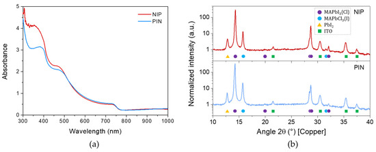
Figure 2.
(a) Absorbance spectra and (b) XRD patterns of the half-cells in the NIP- and PIN-type architectures, i.e., only composed of the perovskite layers grown on np-SnO2 (dark red) and on poly-triarylamine polymer (PTAA) (light blue), respectively.
The two perovskite layers were further characterized with X-ray diffraction (XRD) to better understand their crystalline structure. The diffractograms (see Figure 2b) reveal three different crystalline phases for both NIP- and PIN-based perovskite layers. A first diffraction peak (located here at 2θ = 12.7°) could be associated with the lead iodide (PbI2) phase. This phase might be useful for reducing the grain boundary passivation [61,62]. The main two other phases are an iodide-rich perovskite phase (peak at 14.2°) and a chloride-rich perovskite phase (15.7°). The iodide-rich phase corresponds to the desired MAPbI3 perovskite. Controversy remains on its exact chemical composition, as the Cl from the precursor solution [45] may or may not take part in the MAPbI3 perovskite’s lattice [63]. Some studies have argued in favor of the intercalation of a small amount of chloride atoms within the lattice (resulting in the MAPbI3−xClx notation) [45,64]. Conversely, others have stated that it remains outside the MAPbI3 crystals [65,66] and the perovskite layer [67], at least in the near-surface regions [68]. We thus decided to use the following notation: MAPbI3{Cl}. In addition, Figure S6 supports the idea that in a planar structure, MAPbI3{Cl} crystallizes in a tetragonal phase, in accordance with the literature [63,66]. The addition of chlorine also influences the orientation of the perovskite crystallization along the lattice plane (0): a double diffraction peak may thus be observed around 14.2° and 28.5° (see Figure S6a,b), corresponding to two different crystalline orientations of the tetragonal phase, (00) and (0) [66]. The latter is, here, the preferred orientation for both NIP- and PIN-type architectures. On another note, the observable chloride-rich phase is usually associated with MAPbCl3 [69]. In any case, a huge part of Cl is known to be eliminated from the perovskite layer by the evaporation of the MACl compound during the thermal annealing step, but K. H. Stone et al. revealed that the “PbCl2-derived MAPbI3” formation process occurs from an intermediary compound whose chemical composition was identified to be MA2PbI3Cl. The latter possesses a diffraction ray close to that of the MAPbCl3 perovskite (15.4° versus 15.65° [70], respectively). This newly discovered compound may thus also be present in our perovskite layers. However, according to our diffraction ray position (15.7°), our phase appears to be mostly composed of MAPbCl3, hereinafter noted as MAPbCl3{I}.
According to Figure 2b, the two perovskites (NIP- and PIN-based) have very similar structural properties with rather close crystalline proportions. Thus, even if slight variations in the crystalline proportions can be noticed, indicating a slightly higher amount of the MAPbCl3{I} phase for the PIN-type architecture (6.7% against 4.3%, see Table S2), this does not seem to explain the major differences observed in the absorption for short wavelengths (Figure 2a). Consequently, the above-mentioned difference in optical properties would likely result from the different perovskite layer’s overall density, supported by the fact that more pinholes were observed in the SEM images at the PIN-based perovskite’s surface.
3.2. Comparison of NIP- and PIN-Type Opaque PSCs
The previous characterizations suggest that the perovskite layers in both architectures are quite comparable. J–V acquisitions were then completed in the opaque configuration (without the ITO integration); see NIP-O and PIN-O in Figure 1a. The average results are gathered in Table 1. This set of data was recorded with a shadow mask to best delimitate the illuminated cell’s area (0.131 cm2). Typical J–V curves are displayed in Figure S7a, as are their hysteresis behaviors according to reverse and forward scans (Figure S7b,c). The NIP-O cells have a similar, although slightly better, PCE as compared to the PIN-O cells (10.4% vs. 8.8%). The most noticeable difference between the two architectures is in the FF (63.6 ± 4.1% vs. 54.5 ± 3.4%, respectively). The larger FF for the NIP-O devices could result from better electrical contacts correlating with a lower resistivity in this architecture (see Table 1). This may originate at the interface between the np-SnO2 and the perovskite layer in the PIN-type devices because the SnO2 nanoparticles have merely been “dropped” onto the perovskite layer. This could lead to a non-optimized contact, as compared to a more implemented contact for the NIP-type architecture, where the perovskite conforms to the np-SnO2 surface. Furthermore, we can notice that both the NIP and PIN architectures possesses an important J–V curve hysteresis (Figure S7b,c), which is more pronounced in the case of PIN devices in accordance with a Roc increase and FF decrease (Table 1). A charge accumulation at the interface(s) should be responsible for the hysteresis responses of the devices. According to the literature [71], it seems that this could originate from SnO2, which is well known to give such hysteresis. Proposed alternatives consist of either incorporating an additional layer, e.g., PCBM [72,73], or doping [71,74]. Regarding the more pronounced hysteresis in the PIN-type architecture, this should be related to the same reason as the one mentioned above for the FF decrease. In addition, the lower Jsc measured for the PIN-type cells (18.8 ± 1.1 mA.cm−2 vs. 18.0 ± 0.4 mA.cm−2) likely resulted from the larger absorption of PTAA compared to SnO2. The actual amount of light reaching the active layer would thereby have been decreased.

Table 1.
J–V results (averages) measured in reverse scan mode with an illuminated area of 0.131 cm2 for NIP- and PIN-type opaque perovskite solar cells (PSCs) (the values in brackets are the J–V performance of the champion cells). J–V results are given for campaigns of about twenty cells in total for each architecture. (Roc is the equivalent resistance determined at Voc).
As for the Voc, the PIN-O cells were found to be significantly better (0.902 ± 0.023 V vs. 0.871 ± 0.018 V). This was rather surprising considering the use of the same ETL and HTL for the two architectures as well as the tendency reported in the literature [30] and the previously mentioned direct comparison made by C. Momblona et al. [31]. To elucidate this phenomenon, the perovskites’ photoluminescence was measured. PL was determined both before and after the deposition of the second charge carrier transport layer: PTAA in the NIP-type and np-SnO2 in the PIN-type architecture. Further tests were conducted with the sole addition of the solvents used to deposit the last layer (chlorobenzene and butanols, respectively). The latter measurements were performed to detect the potential effect of the solvent on the previous layer. The corresponding PL spectra are displayed in Figure 3 and show no PL modification before and after spin-coating the pure solvent on the perovskite, regardless of the architecture. On the other hand, surprising antagonistic PL behaviors were found by comparing the NIP- and PIN-type architectures: the PL intensity was quenched after PTAA deposition (NIP case, see Figure 3a) whereas it increased after np-SnO2 deposition (PIN case, Figure 3b). A quenching phenomenon is more likely to be compatible with usual cases, and it is often argued that the decrease in PL intensity comes from charge carrier extraction because of the deposition of an additional extracting layer [75,76]. In our case, the PL acquisitions were performed at Voc, which means that charge carriers could not leave the characterized system [77] but still be transferred to the extracting layer(s). However, charge carrier extraction is very fast (dozens of nanoseconds) [78] when compared to our PL acquisitions’ timescale (few seconds) and therefore might not be observed. Consequently, since defects lead to non-radiative recombination, it is believed, here, that more trap-assisted defects contribute to the PL quenching as observed for the NIP case (Figure 3a). An increase in the defect number after interfacial layer deposition is reported to be the usual tendency [79]. By contrast, a PL increase, as observed for the PIN-type architecture (see Figure 3b), would result in lower trap-assisted defects. This could come from a passivation, for instance, the latter of which also leads to an increase in Voc [78]. We believe that such a passivating effect may likely happen in the PIN-type devices since it would explain the observation of both PL and Voc enhancements. Indeed, it was found that the dispersive agent (the exact chemical formula of which remains unknown) used in the np-SnO2 commercial solution does increase the PL intensity (see Figure S8a). The dispersing agent (within the alcohol mixture) was able to be separated from np-SnO2 by centrifugation (Figure S8b) and was then characterized by NMR after eliminating the solvent. As a result, the NMR spectra (displayed in Figure S8c) reveal amide and siloxane functions for the surfactant(s). Particularly, amide functions have been reported in the literature to possess a passivating property related to their Lewis base feature [80], a category of chemical functions known to passivate perovskite materials [81]. This is an interesting result since it would mean that nanoparticle dispersions could also be customized with a functionalized surfactant to further improve PSCs, for instance.
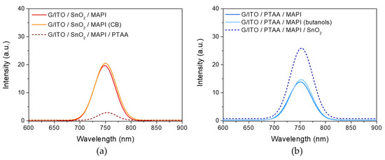
Figure 3.
Photoluminescence (PL) spectra of the CH3NH3PbI3 (MAPI) perovskite obtained from (a) NIP- and (b) PIN-type architectures with three different conditions: stacks up to the perovskite layer, the same stacks above which the n + 1 film was deposited (PTAA for NIP and np-SnO2 for PIN), and, finally, stacks above which only the respective solvent of the corresponding solutions was spin-coated but without any PTAA and np-SnO2.
3.3. Integration of Transparent ITO Electrode in NIP- and PIN-Type Architectures
The integration of the sputtered ITO deposited at room temperature was realized to manufacture semi-transparent PSCs in NIP- and PIN-type architectures. Two distinct devices were first prepared for the two architectures, as illustrated in Figure 1b (see also the photographs in Figure 4a,b). So-called “intermediate cells” were processed: they remained opaque (NIP-int and PIN-int) but included the ITO layer. These cells were used to estimate the compatibility of ITO with the NIP- and PIN-type architectures. Finally, ST devices were made combining this ITO and an openwork metal contact (NIP-ST and PIN-ST). Shadow masks (aperture of 0.131 cm2) were used to avoid potential changes in the illuminated active area, granting a better comparison of all the devices (especially for Jsc), regardless of the illumination side.
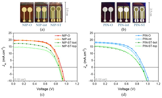
Figure 4.
Pictures of (a) NIP- and (b) PIN-type perovskite devices in the three different configurations for both architectures—opaque, intermediate and semi-transparent cells (from left to right)—and (c,d) their respective J–V curves (“-bot” and “-top” abbreviations stand for an illumination from glass and an illumination from a metal contact, respectively).
Figure 4c,d displays the J–V curves of the cells with the best J–V performances for each NIP- and PIN-type cell. The average J–V data extracted from all the cells are gathered in Table S3 (NIP) and Table S4 (PIN) and are, here, graphically summarized in Figure 5. The very similar behaviors within both the NIP-int and PIN-int devices as compared to the NIP-O and PIN-O devices was first striking to note. In other words, for the two architectures, the ITO addition is relatively well tolerated according to the results obtained from the intermediate cells (Figure 4 and Figure 5). This indicates that both PTAA polymer and the nanoparticles of SnO2 act, to some extent, as a protective layer for the sputtering conditions. This may seem surprising for the latter since a nanoparticle layer is non-dense by nature as compared to the oxide layer usually deposited by atomic layer deposition (ALD), for instance [21]. A small degradation in Jsc is, however, evidenced after ITO integration for the NIP-type architecture (from 18.8 ± 1.1 mA.cm−2 to 17.1 ± 1.4 mA.cm−2, on average), as well as for the PIN-type one, but with a lower magnitude in that case (from 18.0 ± 0.4 mA.cm−2 to 17.7 ± 0.4 mA.cm−2, on average).
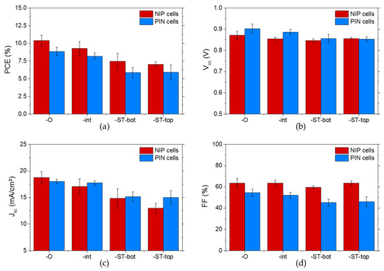
Figure 5.
Averages and standard deviations of J–V data: (a) PCE; (b) Voc; (c) Jsc; (d) FF for NIP- (dark red) and PIN-type (light blue) PSCs of each kind (opaque, intermediate and semi-transparent cells) as well as depending on the illuminated side (“-bot” and “-top” for glass and metal side, respectively). Measurements were done in reverse scan mode with an illuminated area of 0.131 cm2, and J–V results for both NIP- and PIN-type architectures are given for campaigns of about ten cells in total for each device type with indium tin oxide (ITO) and about twenty cells in total without ITO.
The previously observed differences between the NIP- and PIN-type architectures in an opaque configuration and the interpretations described in the previous section are still valid for intermediate and semi-transparent devices, especially for FF and Voc. The additional noticeable diminution of Voc between the opaque and ITO-based configurations is a measurement artifact due to the use of a shadow mask. In the latter case, the surface collection of charge carriers is governed by the ITO film’s surface coverage (about 0.91 cm2) and not by the metal electrode’s one. Thus, the amount of induced shading [82] increases with the addition of the ITO layer. A constant Voc measured without the mask (see Table S5) confirmed that the sputtered ITO layer does not alter the energy alignment and thereby the Voc. In addition, while no significant impact of ITO integration was detected on the FF value for the NIP devices, a slight drop was observed for the PIN-int devices (FF around 52.0 ± 2.7% instead of 54.5 ± 3.4%), and the strongest one, for the PIN-ST devices (FF around 49.9 ± 4.7%, on average). This resulted from several parameters. First, the layers prepared from nanoparticle dispersion (SnO2) tend to develop non-optimized interfaces (whether with perovskite or ITO). Then, the annealing step to improve these interfaces degraded the overall performances in the PIN (not NIP) architecture and was thus not applied for PIN. Finally, fully semi-transparent NIP- and PIN-type devices required the substitution of the electrical contacts. We replaced the opaque metal with an openwork one. As a result, the charge carriers should circulate laterally within the ITO layer before being collected by the metal. This causes an increase in the series resistance in the PIN-ST configurations (see Tables S3 and S4). This resistance combined with the SnO2 upper layer results in a significant reduction in FF for ST-PIN devices.
Consequently, even if the sputtering parameters result from a thorough optimization, further improvements in ITO deposition could still be made to avoid possible electrical mismatches within the stacks. Finely controlling the process parameters of the sputtered ITO is indeed key for achieving increased deposited layers and interface qualities, as well as maximizing optical harvesting by optimizing the thickness. It still remains that the best efficiencies obtained for the NIP- and PIN-type opaque architectures without and with ITO integration are rather close to one another (from 11.9% to 11.1% and from 9.9% to 8.8% for the NIP- and PIN-type architectures, respectively). The absence of metal coverage within the cell’s illuminated area also leads to a notable reduction in Jsc of more than 2 mA.cm−2 with the two architectures (Figure 5c and Tables S3 and S4). The suppression of the metal contact’s mirror effect and the relatively thin perovskite layers (<300 nm), which should be at least 400 nm thick in order to absorb the whole incident luminous flux in the first pass [83], are responsible for this trend. Consequently, partial metal contact involves a decrease in PCE mainly due to these optical losses. This PCE decrease is emphasized in the case of PIN-type cells due to the previously described series resistance.
Focusing on the illumination side, some differences were observed regarding the NIP-ST and PIN-ST devices’ behaviors. A Jsc fall (1.8 mA.cm−2 losses) occurs when the light direction is changed from the glass side (“-bot”) to metal side (“-top”) in the case of NIP-ST devices (see Figure 4c and Figure 5c), while no significant variations (0.2 mA.cm−2 losses) were noticed in the case of PIN-ST cells (see Figure 4d and Figure 5c). This illumination direction dependence originates from the optical properties and transparencies of the glass side and the metal side of the two architectures. Different absorptions between the PTAA and SnO2 materials, their location within the stack (glass or metal side), and differences in the reflection magnitude (air–glass or air–ITO interfaces, as seen in Figure S9a) are cumulative factors implying such a trend. Calculations (using Equation (1)) of the current losses estimated from the transmittances of the four possible operating configurations using the two developed semi-transparent devices (as displayed in Figure 6) are gathered in Table 2 to support this statement.
where q is the elementary charge (C), λ is the wavelength (nm), and ϕAM1.5 is the air mass 1.5 (AM1.5) spectral flux (photons.m−2.s−1.nm−1) obtained from the National Renewable Energy Laboratory [84].
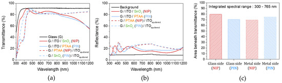
Figure 6.
(a) Transmittance and (b) reflectance curves of the layers that surround the perovskite layer depending on the PSC’s architecture (NIP or PIN) and the illumination side (glass side or metal/ITO side), and (c) the corresponding areas integrated beneath these transmittance curves within the perovskite absorption range (300–765 nm).
Table 2.
Calculated current (Jsc) losses estimated from transmittance measurements (Figure 6) depending on the side of illumination in both NIP- and PIN-type architectures.
Figure 6a,b presents the transparency and reflectivity of the interfacial contacts that surround the perovskite layer in both the selected NIP- and PIN-type architectures for an ST configuration. The glass side illumination for the NIP-type architecture leads to a higher transparency in the perovskite’s absorption range compared to the other ones (regardless of the architecture). The metal side illumination for the PIN-type architecture also shows a good transparency (Figure 6c). Integrations were performed within the interval of 300 nm (λ1) and 765 nm (λ2), which is the overall perovskite’s absorption spectral range. Such an illumination from the metal side of the PIN-type stack allows the effective avoidance of the PTAA’s parasitic absorption.
These calculations remain a first order approximation, mainly because they do not consider the multiple reflections within the ST device’s stack. Nevertheless, the calculation of the optical losses from the electrode to glass side within the same device architecture indicates a loss of about 1.2 mA.cm−2 with the NIP-ST condition, in fair agreement with the experimental observation of 1.8 mA.cm−2. In addition, a slight gain close to 0.3 mA.cm−2 is calculated for PIN-ST condition, which also compares relatively well with the small drop in Jsc obtained from the J–V measurements (0.2 mA.cm−2). Even if this simulation seems to underestimate the real losses determined from J–V acquisitions, it provides both the right tendency and the proper order of magnitude for the amplitude of variations. A good method to enhance the light collection and thereby the photon–electron conversion could be to add an anti-reflection layer. This method would be especially efficient upon the ITO layer (metal side illumination) since higher reflection can be measured from the metal side than the glass side in the whole device (see Figure S9a). As a result, the PIN-type semi-transparent devices retained equivalent PCEs regardless of the illumination side (5.9% on average, and 6.6% and 6.7% for champion cells), whereas the NIP-type devices demonstrated a drop in their efficiency from 9.3% to 7.6% for champion cells (from 7.5% to 7.0% on average) when switching from bottom to top illumination (see Figure 5 and Tables S3 and S4). Thus, for top-side illumination compatible with tandem application, NIP-ST cells remain, in absolute terms, more efficient than PIN-ST cells, even if they possess an intrinsic illumination direction dependence in terms of their efficiency. Nonetheless, the PIN-ST devices yielded better Jsc than the NIP-ST devices, especially with metal side illumination (higher Jsc of around 2 mA.cm−2 on average). This point is of interest for monolithic tandem applications since the current matching between the two tandem’s sub-cells must be maximized to obtain the highest tandem efficiency. Moreover, both the NIP-ST and PIN-ST devices allowed a similar average transmission of about 60% over the 765–1100 nm range (Figure S9b and Table S6), which would correspond to the luminous part available for a bottom sub-cell such as silicon (estimated range: from silicon’s absorption onset, about 1100 nm [85], to perovskite’s one, about 765 nm, as determined here). Therefore, the semi-transparent PIN-type architecture could also have suitable behavior for two-terminal tandem applications.
4. Conclusions
PSCs in both NIP- and PIN-type architectures were elaborated using the same single ETL (np-SnO2) and HTL (PTAA). All the layer depositions could be achieved with an easy-to-scale-up spin-coating process. The resulting perovskite layers’ properties were probed in depth for the two underlying layers. They are optically and microstructurally close to one another, despite a surprising antagonistic PL behavior after the deposition of the transport top layer. The NIP-O and PIN-O reference devices also exhibit analogous efficiencies. The higher FFs observed for NIP-type cells were partly counterbalanced by the systematical higher Voc for the PIN-type cells. The difference in Voc may be related to the uncommon PL behavior, from which a passivation of the perovskite was detected, involving the dispersing agent employed in the np-SnO2 solution. These results pave the way for new methods to process solar cells: two steps at once, combining interfacial nanoparticle layer deposition and system modification (passivation, energy level alignment, surface doping etc.) through a functionalized dispersing agent. In addition, sputtered ITO top-layers were successfully integrated at room temperature as transparent electrodes. This could be done, after optimization, with a relatively low influence on the performance. As a result, this ITO deposition seems to be compatible with perovskites covered by a polymer layer (PTAA) and even those covered by a SnO2 nanoparticle layer implemented using a solution process. This sets the current study apart from the published literature. Upon switching from opaque to semi-transparent PSCs, significant PCE reductions were observed in both architectures. They mainly result from the optical losses related to the absence of the metallic contact’s mirror effect. We also showed by J–V acquisitions that NIP-ST devices present a qualitatively different behavior (especially for Jsc) to their PIN-ST counterparts, depending on the illumination direction. These differences could be satisfactorily quantified with a 1D model of the optical losses, from the transmittance measurements. Even if the NIP-ST devices remain more efficient than their PIN-ST counterparts (with better FFs), the latter still exhibit higher Jsc and better optical properties when illuminated from the metal side. They could therefore be more desirable for monolithic tandem applications.
One should also note that, regardless of the architectures, all the presented devices show efficiencies lower than those of the best cells reported in the current publications. The main goal of the current study was to try and enable some understanding of the mechanisms responsible for the best photovoltaic effects. Additional optimizations such as increasing the perovskite thickness and adding an anti-reflection foil to harvest more photons would be useful. Moreover, modifying our interfacial layers to improve the devices’ electrical features, as well as enhancing the charge extraction at interfaces with perovskite by interface engineering, are future ideas to investigate. Lastly, efforts have also to be focused on expanding this study to mixed-cation and halide perovskites, which generally enable higher efficiencies and stabilities as well as more suitable bandgaps for tandem applications with silicon.
Supplementary Materials
Following supplementary materials are available online at https://www.mdpi.com/1996-1073/13/15/3794/s1. Figure S1. Energy levels of the materials used in both NIP-type and PIN-type stacks. Figure S2. Transmittance curves of PTAA, np-SnO2 and the sputtered ITO used in this study. Figure S3. Tauc plot method applied on absorbance spectra of our NIP (a) and PIN (b) samples in order to determine their respective optical bandgap. Figure S4. Perovskite’s absorption coefficient of NIP- and PIN-type structures. Figure S5. (a) Photography of two PIN samples on which the yellow circles point out several regions with no perovskite deposited on PTAA film due to low wettability of the perovskite precursor solution on PTAA; SEM images of the perovskite layers from NIP-type structure (b) and PIN-type structure (c). Figure S6. Focus on the (a) first order and (b) second order diffraction peaks of MAPbI3 phase revealing the two orientations of MAPbI3{Cl} along (00l) and (hh0). Figure S7. (a) Typical J-V curves of NIP-O devices and PIN-O devices measured in reverse scan; and hysteresis behaviors of (b) NIP-O and (c) PIN-O devices. Figure S8. (a) Normalized PL intensities of the perovskite layer deposited on PTAA film (PIN-type stack) before and after spin-coating of the extracted SnO2 solvent; (b) centrifugation vial showing the extracted solvent fraction; (c) 1H-NMR spectrum of the residue obtained from the extracted solvent fraction after smooth evaporation using a vacuum rotary evaporator. Figure S9. (a) Reflectance curves of the NIP-ST device and PIN-ST device depending on measurements made either on glass side or metal side; and (b) transmittance curves of the same NIP- and PIN-type devices with their corresponding metal side reflectance curves. Table S1. Synthesis of the calculated results obtained from the linear regression of Tauc plot method curves’ linear region. Table S2. Crystalline proportions of crystalline phases within the NIP- and PIN-type perovskite layers. Tables S3 & S4. J-V results achieved in reverse scan with an illuminated area of 0.131 cm2 for respectively NIP and PIN-type perovskite solar cells. Table S5. Voc variations depending on whether the shadow mask is employed or not for NIP- and PIN-type structures with and without ITO. Table S6. Average transparency in the near-IR and visible regions for the NIP-ST device and the PIN-ST device.
Author Contributions
Conceptualization and methodology: S.B., L.F., E.P. and L.P.; T.L. performed the solutions synthesis, the sample fabrication, and the following characterizations: J–V, absorbance, XRD, PL and thickness measurements; these data were analyzed by T.L. with the supervision of L.P., E.P., S.B. and L.F.; the NMR spectrum was generated and analyzed by L.P.; and the SEM images were generated by E.P. The manuscript was written by T.L. and was reviewed by L.P., E.P., S.B. and L.F. All authors have read and agreed to the published version of the manuscript.
Funding
This research was financially supported on the one hand by the USMB and Conseil Savoie Mont Blanc (CSMB) and on the other hand by the Commissariat à l’énergie atomique et aux énergies alternatives (CEA).
Acknowledgments
We thank the National Institute for Solar Energy (INES), the platform of Analyse Structurale (ASTRE) of the Université Savoie Mont Blanc (USMB) and the platform of Consortium des Moyens Technologiques Communs (CMTC) of Grenoble INP for laboratory assistance and laboratory equipment.
Conflicts of Interest
The authors declare no conflict of interest.
References
- Best Research-Cell Efficiency Chart. Available online: https://www.nrel.gov/pv/assets/pdfs/best-research-cell-efficiencies.20200406.pdf (accessed on 30 April 2020).
- Snaith, H.J. Present status and future prospects of perovskite photovoltaics. Nat. Mater. 2018, 17, 372–376. [Google Scholar] [CrossRef] [PubMed]
- Steirer, K.X.; Schulz, P.; Teeter, G.; Stevanovic, V.; Yang, M.; Zhu, K.; Berry, J.J. Defect Tolerance in Methylammonium Lead Triiodide Perovskite. ACS Energy Lett. 2016, 1, 360–366. [Google Scholar] [CrossRef]
- Frohna, K.; Deshpande, T.; Harter, J.; Peng, W.; Barker, B.A.; Neaton, J.B.; Louie, S.G.; Bakr, O.M.; Hsieh, D.; Bernardi, M. Inversion symmetry and bulk Rashba effect in methylammonium lead iodide perovskite single crystals. Nat. Commun. 2018, 9, 1–9. [Google Scholar] [CrossRef] [PubMed]
- Miyata, A.; Mitioglu, A.; Plochocka, P.; Portugall, O.; Wang, J.T.-W.; Stranks, S.D.; Snaith, H.J.; Nicholas, R.J. Direct measurement of the exciton binding energy and effective masses for charge carriers in organic–inorganic tri-halide perovskites. Nat. Phys. 2015, 11, 582–587. [Google Scholar] [CrossRef]
- Wehrenfennig, C.; Eperon, G.E.; Johnston, M.B.; Snaith, H.J.; Herz, L.M. High Charge Carrier Mobilities and Lifetimes in Organolead Trihalide Perovskites. Adv. Mater. 2014, 26, 1584–1589. [Google Scholar] [CrossRef] [PubMed]
- Yang, Y.; Yan, Y.; Yang, M.; Choi, S.; Zhu, K.; Luther, J.M.; Beard, M.C. Low surface recombination velocity in solution-grown CH3NH3PbBr3 perovskite single crystal. Nat. Commun. 2015, 6, 1–6. [Google Scholar] [CrossRef]
- Dong, Q.; Fang, Y.; Shao, Y.; Mulligan, P.; Qiu, J.; Cao, L.; Huang, J. Electron-hole diffusion lengths > 175 mm in solution-grown CH3NH3PbI3 single crystals. Science 2015, 347, 967–970. [Google Scholar] [CrossRef]
- Herz, L.M. Charge-Carrier Mobilities in Metal Halide Perovskites: Fundamental Mechanisms and Limits. ACS Energy Lett. 2017, 2, 1539–1548. [Google Scholar] [CrossRef]
- De Wolf, S.; Holovsky, J.; Moon, S.-J.; Löper, P.; Niesen, B.; Ledinsky, M.; Haug, F.-J.; Yum, J.-H.; Ballif, C. Organometallic Halide Perovskites: Sharp Optical Absorption Edge and Its Relation to Photovoltaic Performance. J. Phys. Chem. Lett. 2014, 5, 1035–1039. [Google Scholar] [CrossRef]
- Ogomi, Y.; Morita, A.; Tsukamoto, S.; Saitho, T.; Fujikawa, N.; Shen, Q.; Toyoda, T.; Yoshino, K.; Pandey, S.S.; Ma, T.; et al. CH3NH3SnxPb(1–x)I3 Perovskite Solar Cells Covering up to 1060 nm. J. Phys. Chem. Lett. 2014, 5, 1004–1011. [Google Scholar] [CrossRef]
- Kitazawa, N.; Watanabe, Y.; Nakamura, Y. Optical properties of CH3NH3PbX3 (X = halogen) and their mixed-halide crystals. J. Mater. Sci. 2002, 37, 3585–3587. [Google Scholar] [CrossRef]
- Noh, J.H.; Im, S.H.; Heo, J.H.; Mandal, T.N.; Seok, S.I. Chemical Management for Colorful, Efficient, and Stable Inorganic–Organic Hybrid Nanostructured Solar Cells. Nano Lett. 2013, 13, 1764–1769. [Google Scholar] [CrossRef] [PubMed]
- Eperon, G.E.; Stranks, S.D.; Menelaou, C.; Johnston, M.B.; Herz, L.M.; Snaith, H.J. Formamidinium lead trihalide: A broadly tunable perovskite for efficient planar heterojunction solar cells. Energy Environ. Sci. 2014, 7, 982. [Google Scholar] [CrossRef]
- Noel, N.K.; Stranks, S.D.; Abate, A.; Wehrenfennig, C.; Guarnera, S.; Haghighirad, A.-A.; Sadhanala, A.; Eperon, G.E.; Pathak, S.K.; Johnston, M.B.; et al. Lead-free organic-inorganic tin halide perovskites for photovoltaic applications. Energy Environ. Sci. 2014, 7, 3061–3068. [Google Scholar] [CrossRef]
- Wali, Q.; Elumalai, N.K.; Iqbal, Y.; Uddin, A.; Jose, R. Tandem perovskite solar cells. Renew. Sustain. Energy Rev. 2018, 84, 89–110. [Google Scholar] [CrossRef]
- Jošt, M.; Kegelmann, L.; Korte, L.; Albrecht, S. Monolithic Perovskite Tandem Solar Cells: A Review of the Present Status and Advanced Characterization Methods Toward 30% Efficiency. Adv. Energy Mater. 2020, 1904102. [Google Scholar] [CrossRef]
- Shen, H.; Walter, D.; Wu, Y.; Fong, K.C.; Jacobs, D.A.; Duong, T.; Peng, J.; Weber, K.; White, T.P.; Catchpole, K.R. Monolithic Perovskite/Si Tandem Solar Cells: Pathways to Over 30% Efficiency. Adv. Energy Mater. 2019, 10, 1902840. [Google Scholar] [CrossRef]
- Bush, K.A.; Manzoor, S.; Frohna, K.; Yu, Z.J.; Raiford, J.A.; Palmstrom, A.F.; Wang, H.-P.; Prasanna, R.; Bent, S.F.; Holman, Z.C.; et al. Minimizing Current and Voltage Losses to Reach 25% Efficient Monolithic Two-Terminal Perovskite-Silicon Tandem Solar Cells. ACS Energy Lett. 2018, 3, 2173–2180. [Google Scholar] [CrossRef]
- Jošt, M.; Köhnen, E.; Morales-Vilches, A.B.; Lipovšek, B.; Jäger, K.; Macco, B.; Al-Ashouri, A.; Krč, J.; Korte, L.; Rech, B.; et al. Textured interfaces in monolithic perovskite/silicon tandem solar cells: Advanced light management for improved efficiency and energy yield. Energy Environ. Sci. 2018, 11, 3511–3523. [Google Scholar] [CrossRef]
- Sahli, F.; Werner, J.; Kamino, B.A.; Bräuninger, M.; Monnard, R.; Paviet-Salomon, B.; Barraud, L.; Ding, L.; Diaz Leon, J.J.; Sacchetto, D.; et al. Fully textured monolithic perovskite/silicon tandem solar cells with 25.2% power conversion efficiency. Nat. Mater. 2018, 17, 820–826. [Google Scholar] [CrossRef]
- Ramírez Quiroz, C.O.; Shen, Y.; Salvador, M.; Forberich, K.; Schrenker, N.; Spyropoulos, G.D.; Heumüller, T.; Wilkinson, B.; Kirchartz, T.; Spiecker, E.; et al. Balancing electrical and optical losses for efficient 4-terminal Si—perovskite solar cells with solution processed percolation electrodes. J. Mater. Chem. A 2018, 6, 3583–3592. [Google Scholar] [CrossRef]
- Shockley, W.; Queisser, H.J. Detailed Balance Limit of Efficiency of p-n Junction Solar Cells. J. Appl. Phys. 1961, 32, 510–519. [Google Scholar] [CrossRef]
- Kojima, A.; Teshima, K.; Shirai, Y.; Miyasaka, T. Organometal Halide Perovskites as Visible-Light Sensitizers for Photovoltaic Cells. J. Am. Chem. Soc. 2009, 131, 6050–6051. [Google Scholar] [CrossRef]
- Jeng, J.-Y.; Chiang, Y.-F.; Lee, M.-H.; Peng, S.-R.; Guo, T.-F.; Chen, P.; Wen, T.-C. CH3NH3PbI3 Perovskite/Fullerene Planar-Heterojunction Hybrid Solar Cells. Adv. Mater. 2013, 25, 3727–3732. [Google Scholar] [CrossRef] [PubMed]
- Yang, W.S.; Park, B.-W.; Jung, E.H.; Jeon, N.J.; Kim, Y.C.; Lee, D.U.; Shin, S.S.; Seo, J.; Kim, E.K.; Noh, J.H.; et al. Iodide management in formamidinium-lead-halide—Based perovskite layers for efficient solar cells. Science 2017, 356, 1376–1379. [Google Scholar] [CrossRef] [PubMed]
- Al-Ashouri, A.; Magomedov, A.; Roß, M.; Jošt, M.; Talaikis, M.; Chistiakova, G.; Bertram, T.; Márquez, J.A.; Köhnen, E.; Kasparavičius, E.; et al. Conformal monolayer contacts with lossless interfaces for perovskite single junction and monolithic tandem solar cells. Energy Environ. Sci. 2019, 12, 3356–3369. [Google Scholar] [CrossRef]
- Green, M.A.; Dunlop, E.D.; Hohl-Ebinger, J.; Yoshita, M.; Kopidakis, N.; Ho-Baillie, A.W.Y. Solar cell efficiency tables (Version 55). Prog. Photovolt. Res. Appl. 2020, 28, 3–15. [Google Scholar] [CrossRef]
- Conings, B.; Babayigit, A.; Klug, M.T.; Bai, S.; Gauquelin, N.; Sakai, N.; Wang, J.T.-W.; Verbeeck, J.; Boyen, H.-G.; Snaith, H.J. A Universal Deposition Protocol for Planar Heterojunction Solar Cells with High Efficiency Based on Hybrid Lead Halide Perovskite Families. Adv. Mater. 2016, 28, 10701–10709. [Google Scholar] [CrossRef] [PubMed]
- Luo, D.; Yang, W.; Wang, Z.; Sadhanala, A.; Hu, Q.; Su, R.; Shivanna, R.; Trindade, G.F.; Watts, J.F.; Xu, Z.; et al. Enhanced photovoltage for inverted planar heterojunction perovskite solar cells. Science 2018, 360, 1442–1446. [Google Scholar] [CrossRef]
- Momblona, C.; Gil-Escrig, L.; Bandiello, E.; Hutter, E.M.; Sessolo, M.; Lederer, K.; Blochwitz-Nimoth, J.; Bolink, H.J. Efficient vacuum deposited p-i-n and n-i-p perovskite solar cells employing doped charge transport layers. Energy Environ. Sci. 2016, 9, 3456–3463. [Google Scholar] [CrossRef]
- Bai, Y.; Meng, X.; Yang, S. Interface Engineering for Highly Efficient and Stable Planar p-i-n Perovskite Solar Cells. Adv. Energy Mater. 2018, 8, 1701883. [Google Scholar] [CrossRef]
- Xu, J.; Buin, A.; Ip, A.H.; Li, W.; Voznyy, O.; Comin, R.; Yuan, M.; Jeon, S.; Ning, Z.; McDowell, J.J.; et al. Perovskite-fullerene hybrid materials suppress hysteresis in planar diodes. Nat. Commun. 2015, 6. [Google Scholar] [CrossRef] [PubMed]
- Bailie, C.D.; McGehee, M.D. High-efficiency tandem perovskite solar cells. MRS Bull. 2015, 40, 681–686. [Google Scholar] [CrossRef]
- Fu, F.; Feurer, T.; Weiss, T.P.; Pisoni, S.; Avancini, E.; Andres, C.; Buecheler, S.; Tiwari, A.N. High-efficiency inverted semi-transparent planar perovskite solar cells in substrate configuration. Nat. Energy 2017, 2, 1–9. [Google Scholar] [CrossRef]
- Fan, L.; Li, Y.; Yao, X.; Ding, Y.; Zhao, S.; Shi, B.; Wei, C.; Zhang, D.; Li, B.; Wang, G.; et al. Delayed Annealing Treatment for High-Quality CuSCN: Exploring Its Impact on Bifacial Semitransparent n-i-p Planar Perovskite Solar Cells. ACS Appl. Energy Mater. 2018, 1, 1575–1584. [Google Scholar] [CrossRef]
- Pang, S.; Li, X.; Dong, H.; Chen, D.; Zhu, W.; Chang, J.; Lin, Z.; Xi, H.; Zhang, J.; Zhang, C.; et al. Efficient Bifacial Semitransparent Perovskite Solar Cells Using Ag/V2O5 as Transparent Anodes. ACS Appl. Mater. Interfaces 2018, 10, 12731–12739. [Google Scholar] [CrossRef]
- Wei, Z.; Smith, B.; De Rossi, F.; Searle, J.R.; Worsley, D.A.; Watson, T.M. Efficient and semi-transparent perovskite solar cells using a room-temperature processed MoOx/ITO/Ag/ITO electrode. J. Mater. Chem. C 2019, 7, 10981–10987. [Google Scholar] [CrossRef]
- Han, K.; Xie, M.; Zhang, L.; Yan, L.; Wei, J.; Ji, G.; Luo, Q.; Lin, J.; Hao, Y.; Ma, C.-Q. Fully solution processed semi-transparent perovskite solar cells with spray-coated silver nanowires/ZnO composite top electrode. Sol. Energy Mater. Sol. Cells 2018, 185, 399–405. [Google Scholar] [CrossRef]
- Jiang, Q.; Zhang, X.; You, J. SnO2: A Wonderful Electron Transport Layer for Perovskite Solar Cells. Small 2018, 14, 1–14. [Google Scholar] [CrossRef]
- Watson, B.L.; Rolston, N.; Bush, K.A.; Taleghani, L.; Dauskardt, R.H. Synthesis and use of a hyper-connecting cross-linking agent in the hole-transporting layer of perovskite solar cells. J. Mater. Chem. A 2017, 5, 19267–19279. [Google Scholar] [CrossRef]
- Zhu, M.; Liu, W.; Ke, W.; Clark, S.; Secor, E.B.; Song, T.-B.; Kanatzidis, M.G.; Li, X.; Hersam, M.C. Millisecond-pulsed photonically-annealed tin oxide electron transport layers for efficient perovskite solar cells. J. Mater. Chem. A 2017, 5, 24110–24115. [Google Scholar] [CrossRef]
- Spalla, M.; Planes, E.; Perrin, L.; Matheron, M.; Berson, S.; Flandin, L. Alternative Electron Transport Layer Based on Al-Doped ZnO and SnO2 for Perovskite Solar Cells: Impact on Microstructure and Stability. ACS Appl. Energy Mater. 2019, 2, 7183–7195. [Google Scholar] [CrossRef]
- Shaikh, J.S.; Shaikh, N.S.; Sheikh, A.D.; Mali, S.S.; Kale, A.J.; Kanjanaboos, P.; Hong, C.K.; Kim, J.H.; Patil, P.S. Perovskite solar cells: In pursuit of efficiency and stability. Mater. Des. 2017, 136, 54–80. [Google Scholar] [CrossRef]
- Colella, S.; Mosconi, E.; Fedeli, P.; Listorti, A.; Gazza, F.; Orlandi, F.; Ferro, P.; Besagni, T.; Rizzo, A.; Calestani, G.; et al. MAPbI3−xClx Mixed Halide Perovskite for Hybrid Solar Cells: The Role of Chloride as Dopant on the Transport and Structural Properties. Chem. Mater. 2013, 25, 4613–4618. [Google Scholar] [CrossRef]
- Correa Baena, J.P.; Steier, L.; Tress, W.; Saliba, M.; Neutzner, S.; Matsui, T.; Giordano, F.; Jacobsson, T.J.; Srimath Kandada, A.R.; Zakeeruddin, S.M.; et al. Highly efficient planar perovskite solar cells through band alignment engineering. Energy Environ. Sci. 2015, 8, 2928–2934. [Google Scholar] [CrossRef]
- Aygüler, M.F.; Hufnagel, A.G.; Rieder, P.; Wussler, M.; Jaegermann, W.; Bein, T.; Dyakonov, V.; Petrus, M.L.; Baumann, A.; Docampo, P. Influence of Fermi Level Alignment with Tin Oxide on the Hysteresis of Perovskite Solar Cells. ACS Appl. Mater. Interfaces 2018, 10, 11414–11419. [Google Scholar] [CrossRef]
- Brinkmann, K.O.; Zhao, J.; Pourdavoud, N.; Becker, T.; Hu, T.; Olthof, S.; Meerholz, K.; Hoffmann, L.; Gahlmann, T.; Heiderhoff, R.; et al. Suppressed decomposition of organometal halide perovskites by impermeable electron-extraction layers in inverted solar cells. Nat. Commun. 2017, 8, 1–9. [Google Scholar] [CrossRef]
- Khadka, D.B.; Shirai, Y.; Yanagida, M.; Ryan, J.W.; Miyano, K. Exploring the effects of interfacial carrier transport layers on device performance and optoelectronic properties of planar perovskite solar cells. J. Mater. Chem. C 2017, 5, 8819–8827. [Google Scholar] [CrossRef]
- Hawash, Z.; Ono, L.K.; Qi, Y. Recent Advances in Spiro-MeOTAD Hole Transport Material and Its Applications in Organic-Inorganic Halide Perovskite Solar Cells. Adv. Mater. Interfaces 2018, 5, 1–22. [Google Scholar] [CrossRef]
- Zardetto, V.; Williams, B.L.; Perrotta, A.; Di Giacomo, F.; Verheijen, M.A.; Andriessen, R.; Kessels, W.M.M.; Creatore, M. Atomic layer deposition for perovskite solar cells: Research status, opportunities and challenges. Sustain. Energy Fuels 2017, 1, 30–55. [Google Scholar] [CrossRef]
- Boix, P.P.; Nonomura, K.; Mathews, N.; Mhaisalkar, S.G. Current progress and future perspectives for organic/inorganic perovskite solar cells. Mater. Today 2014, 17, 16–23. [Google Scholar] [CrossRef]
- Xu, F.; Zhang, T.; Li, G.; Zhao, Y. Synergetic Effect of Chloride Doping and CH3NH3PbCl3 on CH3NH3PbI3−xClx Perovskite-Based Solar Cells. ChemSusChem 2017, 10, 2365–2369. [Google Scholar] [CrossRef] [PubMed]
- Tian, Y.; Scheblykin, I.G. Artifacts in Absorption Measurements of Organometal Halide Perovskite Materials: What Are the Real Spectra? J. Phys. Chem. Lett. 2015, 6, 3466–3470. [Google Scholar] [CrossRef] [PubMed]
- Bi, C.; Wang, Q.; Shao, Y.; Yuan, Y.; Xiao, Z.; Huang, J. Non-wetting surface-driven high-aspect-ratio crystalline grain growth for efficient hybrid perovskite solar cells. Nat. Commun. 2015, 6, 1–7. [Google Scholar] [CrossRef]
- You, J.; Guo, F.; Qiu, S.; He, W.; Wang, C.; Liu, X.; Xu, W.; Mai, Y. The fabrication of homogeneous perovskite films on non-wetting interfaces enabled by physical modification. J. Energy Chem. 2019, 38, 192–198. [Google Scholar] [CrossRef]
- Xu, X.; Ma, C.; Cheng, Y.; Xie, Y.-M.; Yi, X.; Gautam, B.; Chen, S.; Li, H.-W.; Lee, C.-S.; So, F.; et al. Ultraviolet-ozone surface modification for non-wetting hole transport materials based inverted planar perovskite solar cells with efficiency exceeding 18%. J. Power Sour. 2017, 360, 157–165. [Google Scholar] [CrossRef]
- Spalla, M.; Perrin, L.; Planès, E.; Matheron, M.; Berson, S.; Flandin, L. Influence of Chloride/Iodide Ratio in MAPbI3-xClx Perovskite Solar Devices: Case of Low Temperature Processable AZO Sub-Layer. Energies 2020, 13, 1927. [Google Scholar] [CrossRef]
- Park, B.; Philippe, B.; Gustafsson, T.; Sveinbjörnsson, K.; Hagfeldt, A.; Johansson, E.M.J.; Boschloo, G. Enhanced Crystallinity in Organic–Inorganic Lead Halide Perovskites on Mesoporous TiO2 via Disorder-Order Phase Transition. Chem. Mater. 2014, 26, 4466–4471. [Google Scholar] [CrossRef]
- Stamplecoskie, K.G.; Manser, J.S.; Kamat, P.V. Dual nature of the excited state in organic–inorganic lead halide perovskites. Energy Environ. Sci. 2015, 8, 208–215. [Google Scholar] [CrossRef]
- Chen, Q.; Zhou, H.; Song, T.-B.; Luo, S.; Hong, Z.; Duan, H.-S.; Dou, L.; Liu, Y.; Yang, Y. Controllable Self-Induced Passivation of Hybrid Lead Iodide Perovskites toward High Performance Solar Cells. Nano Lett. 2014, 14, 4158–4163. [Google Scholar] [CrossRef]
- Shukla, S.; Shukla, S.; Haur, L.J.; Dintakurti, S.S.H.; Han, G.; Priyadarshi, A.; Baikie, T.; Mhaisalkar, S.G.; Mathews, N. Effect of Formamidinium/Cesium Substitution and PbI2 on the Long-Term Stability of Triple-Cation Perovskites. ChemSusChem 2017, 10, 3804–3809. [Google Scholar] [CrossRef]
- Wang, Q.; Lyu, M.; Zhang, M.; Yun, J.-H.; Chen, H.; Wang, L. Transition from the Tetragonal to Cubic Phase of Organohalide Perovskite: The Role of Chlorine in Crystal Formation of CH3NH3PbI3onTiO2 Substrates. J. Phys. Chem. Lett. 2015, 6, 4379–4384. [Google Scholar] [CrossRef] [PubMed]
- Pool, V.L.; Gold-Parker, A.; McGehee, M.D.; Toney, M.F. Chlorine in PbCl2-Derived Hybrid-Perovskite Solar Absorbers. Chem. Mater. 2015, 27, 7240–7243. [Google Scholar] [CrossRef]
- Chen, Q.; Zhou, H.; Fang, Y.; Stieg, A.Z.; Song, T.-B.; Wang, H.-H.; Xu, X.; Liu, Y.; Lu, S.; You, J.; et al. The optoelectronic role of chlorine in CH3NH3PbI3(Cl)-based perovskite solar cells. Nat. Commun. 2015, 6, 7269. [Google Scholar] [CrossRef] [PubMed]
- Dally, P. Cellules Solaires à base de Matériaux Pérovskites: De la Caractérisation des matériaux à L’amélioration des Rendements et de la Stabilité. Matériaux, Mécanique, Génie civil, Electrochimie; Université Grenoble Alpes: Le Bourget-du-Lac, France, 2019. [Google Scholar]
- Dar, M.I.; Arora, N.; Gao, P.; Ahmad, S.; Grätzel, M.; Nazeeruddin, M.K. Investigation Regarding the Role of Chloride in Organic–Inorganic Halide Perovskites Obtained from Chloride Containing Precursors. Nano Lett. 2014, 14, 6991–6996. [Google Scholar] [CrossRef] [PubMed]
- Starr, D.E.; Sadoughi, G.; Handick, E.; Wilks, R.G.; Alsmeier, J.H.; Köhler, L.; Gorgoi, M.; Snaith, H.J.; Bär, M. Direct observation of an inhomogeneous chlorine distribution in CH3NH3PbI3−xClx layers: Surface depletion and interface enrichment. Energy Environ. Sci. 2015, 8, 1609–1615. [Google Scholar] [CrossRef]
- Stone, K.H.; Gold-Parker, A.; Pool, V.L.; Unger, E.L.; Bowring, A.R.; McGehee, M.D.; Toney, M.F.; Tassone, C.J. Transformation from crystalline precursor to perovskite in PbCl2-derived MAPbI3. Nat. Commun. 2018, 9, 3458. [Google Scholar] [CrossRef]
- Cheng, X.; Jing, L.; Zhao, Y.; Du, S.; Ding, J.; Zhou, T. Crystal orientation-dependent optoelectronic properties of MAPbCl 3 single crystals. J. Mater. Chem. C 2018, 6, 1579–1586. [Google Scholar] [CrossRef]
- Luan, Y.; Yi, X.; Mao, P.; Wei, Y.; Zhuang, J.; Chen, N.; Lin, T.; Li, C.; Wang, J. High-Performance Planar Perovskite Solar Cells with Negligible Hysteresis Using 2,2,2-Trifluoroethanol-Incorporated SnO2. iScience 2019, 16, 433–441. [Google Scholar] [CrossRef]
- Chen, Y.; Xu, C.; Xiong, J.; Zhang, Z.; Zhang, X.; Yang, J.; Xue, X.; Yang, D.; Zhang, J. Benefits of fullerene/SnO2 bilayers as electron transport layer for efficient planar perovskite solar cells. Organ. Electron. 2018, 58, 294–300. [Google Scholar] [CrossRef]
- Wang, J.; Datta, K.; Weijtens, C.H.L.; Wienk, M.M.; Janssen, R.A.J. Insights into Fullerene Passivation of SnO2 Electron Transport Layers in Perovskite Solar Cells. Adv. Funct. Mater. 2019, 29, 1905883. [Google Scholar] [CrossRef]
- Ma, Z.; Zhou, W.; Xiao, Z.; Zhang, H.; Li, Z.; Zhuang, J.; Peng, C.; Huang, Y. Negligible hysteresis planar perovskite solar cells using Ga-doped SnO2 nanocrystal as electron transport layers. Organ. Electron. 2019, 71, 98–105. [Google Scholar] [CrossRef]
- Zhu, Z.; Bai, Y.; Liu, X.; Chueh, C.-C.; Yang, S.; Jen, A.K.-Y. Enhanced Efficiency and Stability of Inverted Perovskite Solar Cells Using Highly Crystalline SnO2 Nanocrystals as the Robust Electron-Transporting Layer. Adv. Mater. 2016, 28, 6478–6484. [Google Scholar] [CrossRef] [PubMed]
- Benhattab, S.; Cho, A.-N.; Nakar, R.; Berton, N.; Tran-Van, F.; Park, N.-G.; Schmaltz, B. Simply designed carbazole-based hole transporting materials for efficient perovskite solar cells. Organ. Electron. 2018, 56, 27–30. [Google Scholar] [CrossRef]
- Stolterfoht, M.; Le Corre, V.M.; Feuerstein, M.; Caprioglio, P.; Koster, L.J.A.; Neher, D. Voltage-Dependent Photoluminescence and How It Correlates with the Fill Factor and Open-Circuit Voltage in Perovskite Solar Cells. ACS Energy Lett. 2019, 4, 2887–2892. [Google Scholar] [CrossRef]
- Stolterfoht, M.; Wolff, C.M.; Márquez, J.A.; Zhang, S.; Hages, C.J.; Rothhardt, D.; Albrecht, S.; Burn, P.L.; Meredith, P.; Unold, T.; et al. Visualization and suppression of interfacial recombination for high-efficiency large-area pin perovskite solar cells. Nat. Energy 2018, 3, 847–854. [Google Scholar] [CrossRef]
- Stolterfoht, M.; Caprioglio, P.; Wolff, C.M.; Márquez, J.A.; Nordmann, J.; Zhang, S.; Rothhardt, D.; Hörmann, U.; Amir, Y.; Redinger, A.; et al. The impact of energy alignment and interfacial recombination on the internal and external open-circuit voltage of perovskite solar cells. Energy Environ. Sci. 2019, 12, 2778–2788. [Google Scholar] [CrossRef]
- Wang, S.-Y.; Chen, C.-P.; Chung, C.-L.; Hsu, C.-W.; Hsu, H.-L.; Wu, T.-H.; Zhuang, J.-Y.; Chang, C.-J.; Chen, H.M.; Chang, Y.J. Defect Passivation by Amide-Based Hole-Transporting Interfacial Layer Enhanced Perovskite Grain Growth for Efficient p–i–n Perovskite Solar Cells. ACS Appl. Mater. Interfaces 2019, 11, 40050–40061. [Google Scholar] [CrossRef]
- Noel, N.K.; Abate, A.; Stranks, S.D.; Parrott, E.S.; Burlakov, V.M.; Goriely, A.; Snaith, H.J. Enhanced Photoluminescence and Solar Cell Performance via Lewis Base Passivation of Organic-Inorganic Lead Halide Perovskites. ACS Nano 2014, 8, 9815–9821. [Google Scholar] [CrossRef]
- Quaschning, V.; Hanitsch, R. Influence of shading on electrical parameters of solar cells. In Proceedings of the Conference Record of the Twenty Fifth IEEE Photovoltaic Specialists Conference, Washington, DC, USA, 13 May 1996; IEEE: Washington, DC, USA, 1996; pp. 1287–1290. [Google Scholar]
- Yang, W.S.; Noh, J.H.; Jeon, N.J.; Kim, Y.C.; Ryu, S.; Seo, J.; Seok, S.I. High-performance photovoltaic perovskite layers fabricated through intramolecular exchange. Science 2015, 348, 1234–1237. [Google Scholar] [CrossRef]
- Reference Solar Spectral Irradiance: ASTM G-173. Available online: https://rredc.nrel.gov/solar//spectra/am1.5/ASTMG173/ASTMG173.html (accessed on 24 May 2019).
- Thurmond, C.D. The Standard Thermodynamic Functions for the Formation of Electrons and Holes in Ge, Si, GaAs, and GaP. J. Electrochem. Soc. 1975, 122, 1133. [Google Scholar] [CrossRef]


© 2020 by the authors. Licensee MDPI, Basel, Switzerland. This article is an open access article distributed under the terms and conditions of the Creative Commons Attribution (CC BY) license (http://creativecommons.org/licenses/by/4.0/).