Abstract
The operational expenditures of solar energy are gaining attention because of the continuous decrease of the capital expenditures. This creates a demand for more reliable systems to further decrease the costs. Increased reliability is often ensured by iterative use of design for reliability. The number of iterations that can take place strongly depends on the computational efficiency of this methodology. The main research objective is to quantify the influence of the temperature dependence of the electrical variables used in the electro-thermal model on the reliability and the computation time. The influence on the reliability is evaluated by using a 2-D finite elements method model of the MOSFET and calculating the plastic energy dissipation density in the die-attach and the bond wire. The trade-off between computation time of the electro-thermal model in PLECS (4.3, Plexim, Zurich, Switzerland) and generated plastic energy accuracy obtained in COMSOL (5.3, COMSOL Inc., Burlington, MA, USA) is reported when excluding a certain temperature dependence. The results indicate that the temperature dependence of the input and output capacitors causes no change in the plastic energy dissipated in the MOSFET but does introduce the largest increase in computation time. However, not including the temperature dependence of the MOSFET itself generates the largest difference in plastic energy of 10% as the losses in the die are underestimated.
1. Introduction
Renewable energy sources currently make up 28% of the global electricity generation (including hydro) and this is expected to rise towards 45% by 2040 [1]. The share of solar energy is currently only 4%, but it is considered the fastest growing electricity source due to a 40% increase in the compound annual growth rate (CAGR) over the last 15 years [2]. One of the main reasons for this exceptional growth is the continuous decrease in the levelized cost of electricity (LCOE) [3]. This decrease is mainly a result of the declining trend in manufacturing costs of the photovoltaic (PV) modules which represent a large part of the investment expenditures (CAPEX). These investment costs currently make up 75% of the LCOE with the other 25% allocated to operational and maintenance expenditures (OPEX) [4]. As the CAPEX continues to decrease, the weight of the OPEX will start to increase which will shift the focus more towards increasing the reliability and lifetime of the solar energy system in order to further reduce the LCOE. As reported in [5], 60% of unscheduled maintenance costs are caused by failures occurring within the power electronics of the power conversion stage. In the majority of the cases, these failures are caused by the degradation of the packaging materials used for the switching devices which are exposed to large amounts of thermo-mechanical stress generated by the high operating temperatures and the large discrepancies in coefficients of thermal expansion (CTE) between the material layers [6,7,8,9,10,11]. A condition monitoring setup can provide insights into the degradation behavior of several electrical and thermal parameters of the power electronics during the operating conditions [12,13]. This process, however slow, provides the most valuable data over a long period of time to further improve the design of the individual components and the converter. Alternatively, highly accelerated stress testing is performed to reduce the amount of time for the degradation to occur but at the cost of potentially triggering failure mechanisms that would normally not occur during operating conditions [14,15]. Both of these techniques can provide an input for the design process to further enhance their design in order to increase the reliability but at a significant financial cost. A cheaper and faster method lies in applying design for reliability (DfR), an iterative design process (depicted in Figure 1) which prioritizes reliability [16,17]. This methodology quickly and accurately investigates the sensitivity of the design to several external inputs in order to propose more reliable design adaptations. A combination of constructing an electro-thermal model of the used topology and constructing a finite elements method (FEM) model of the most failure-prone component [18] is often adopted but other methods which employ empirical lifetime models are also used for their computational efficiency [19]. In either case, constructing an electro-thermal model of a photovoltaic DC–DC converter is the first step in understanding the thermo-mechanical stress generated inside of the individual components. Various literature is available on the different methods of creating the electro-thermal model of an electrical circuit although every single method is based on several assumptions [20,21,22]. The electrical part can be expanded with multiple levels of detail as every component has several parasitic inductances, capacitances and resistances in either series or parallel [23]. The amount of parasitics included depends mostly on the application of the model. For reliability analyses, the parasitic series resistances are only considered as they contribute towards heat generation through Joule heating [24]. The thermal part can be expanded towards a 3-D heat diffusion model for every component [25] or can be simplified to a 1-D lumped thermal network that interconnects all of components on the PCB [26]. Not only is the heat generation and coupling of each component on the printed circuit board (PCB) included into the electro-thermal model, but also the temperature dependence of the electrical variables such as the capacitances, the parasitic series resistances and the solar panel itself [17]. Including these temperature dependences contributes towards either increasing or decreasing the overall computational efficiency of this methodology. Therefore, appropriate sensitivity analyses are required to quantify the respective trade-offs between the gain in accuracy and computation time. This paper reports and quantifies these trade-offs in order for circuit designers to determine whether they have to include these levels of detail in their DfR methodology or can neglect them in order to reduce the overall computation time.
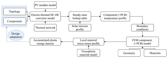
Figure 1.
The Design for Reliability methodology applied to photovoltaic DC/DC converters [17].
The methodology used to perform the required sensitivity analyses is depicted in Figure 2 together with the structure of the paper. Firstly, in Section 2, an electro-thermal model is constructed based on an interleaved boost converter used in photovoltaic applications. The model is based on the datasheets of the respective components as well as a few assumptions regarding the thermal network. Electro-thermal coupling and maximum power point tracking (MPPT) are also implemented. In Section 3, the constructed model is validated by creating a steady state lookup table from experimental testing. In Section 4, a FEM model is constructed of the used MOSFET based on X-raying imaging in order to calculate the difference in accuracy in generated stress in the form of plastic dissipation energy density. In Section 5, the trade-offs between the computation time of the electro-thermal model and the plastic energy generated in the MOSFET for not including the temperature dependence of a certain electrical variable are reported. Lastly, Section 6 draws the conclusion.
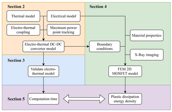
Figure 2.
Flowchart of the paper methodology and structure.
2. Electro-Thermal Model of the Photovoltaic DC/DC Converter
As stated in the introduction section, constructing an electro-thermal model of a certain circuit topology is the first step in order to quantify the thermo-mechanical stress generated inside each component. Apart from the base components with their respective values, the electrical part can be expanded with multiple levels of detail in the form of parasitic elements. For the thermal part, the three main thermal paths, namely conductive, convective and radiative heat transfer, need to be considered for each component as well as the temperature dependence of each electrical variable. Finally, a maximum power point tracking algorithm and control system need to be implemented in order to adjust the duty cycle of the switching devices for a certain combination of solar panel irradiance and ambient temperature. The electro-thermal model is implemented using PLECS Blockset (4.3, Plexim, Zurich, Switzerland) and Simulink (9.3, MathWorks, Natick, MA, USA).
2.1. Electrical
The electrical model is constructed based on a three-leg interleaved boost converter for photovoltaic applications depicted in Figure 3. This topology stands out in terms of reliability when compared to the traditional boost converter due to the built-in redundancy and the ability to distribute the thermal stresses among all parallel components [27]. This topology also reduces the input and output ripple current and in turn, fewer capacitors are required to smoothen out the input and output voltage. In terms of parasitic elements, there are multiple levels of detail that can be added for each component in the form of inductances, capacitances or resistances in either series or parallel [23]. Only the parasitic series resistances are taken into account as they conduct the nominal current and are therefore the main sources of heat generation as a consequence of Joule heating. This includes the DC resistance of each inductor, the equivalent series resistance of each capacitor, the drain-source on-resistance of each MOSFET and the on-resistance of each diode. The converter is designed to boost the input voltage of a 200 W crystalline silicon solar panel from 30 V to 100 V at a switching frequency of 100 kHz. The pulse width modulation (PWM) signal arriving at the gates of the MOSFETs is also phase-shifted by a third of the switching period per leg in order to further reduce the ripple current at the input and the output. The components together with their key parameters and series resistance at standard test conditions (STC) used in the topology are listed in Table 1.
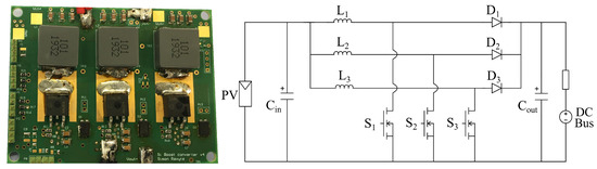
Figure 3.
Photograph (left) of the printed circuit board assembly and the schematic (right) of a three-leg interleaved boost converter for photovoltaic applications.

Table 1.
The components used in the interleaved boost converter together with their key parameters and series resistance.
2.2. Thermal
The steady state Foster thermal network implemented in the electro-thermal model is shown in Figure 4 as an equivalent electrical circuit in which the temperature is equal to the voltage and the heat losses are replaced by current sources [26]. It is supported by several assumptions reported in previous work [28,29]. Here, the main purpose of the electro-thermal model is to create steady state temperature lookup tables for various components in order to translate mission profiles and perform reliability analyses [17]. For this reason, all thermal capacitances in the thermal network are disabled as this greatly reduces the required computation time to reach the steady state. As mentioned in the previous subsection, the main heat source for each component is the joule heating or conduction losses generated by current flowing through the component’s respective parasitic series resistance. In addition to this, the switching devices also generate heat through their switching losses for which the calculation methods can be found in [30]. The thermal network assumes a single conductive thermal resistance in between the component’s heat source and its case. Next, the heat can either be transferred into the surrounding air through the convective thermal resistance or into the PCB through another conductive thermal resistance. Both of these mediums are considered as heat sinks that redistribute the heat among the connected components. Finally, the PCB can transfer its heat into the air through a final convective thermal resistance. In order to include the effect of radiative heat transfer, the convective heat transfer coefficient h in still air (natural convection) was slightly oversized according to [31]. Equation (1) displays the formula used to calculate the conductive thermal resistance with d the thickness of the material, k the thermal conductivity of the material and A the cross-sectional surface area. Equation (2) displays the formula used to calculate the convective thermal resistance with h being the convective heat transfer coefficient and A being the cross-sectional surface area. Table 2 lists the calculated thermal resistances used in the thermal network. If a certain value was provided through the component’s datasheet, then that value is adopted instead. The temperature dependence nor the degradation dependence of these values is included as it falls outside of the scope of this paper.
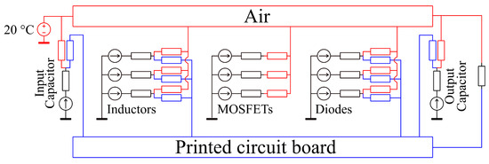
Figure 4.
Steady state Foster thermal network of a three-leg interleaved boost converter.
Table 2.
The thermal resistances for the heat transfer of the converter’s components and PCB used in the thermal network of Figure 4.
2.3. ElectroThermal Coupling
In the previous two subsections, both the electrical model and the thermal model were discussed separately. Although the thermal model is based on the heat generated by the electrical components, the influence of the temperature on the electrical variables, which is the main focus of this paper, still has to be implemented. The chosen approach is based on 1-D lookup tables that can be extracted from the datasheet of the respective component. In practice, every temperature dependent electrical variable is updated through the connected lookup table for every switching period until the relative tolerance of the simulation is reached. In this topology, there is a lookup table for the temperature dependence of every inductance of the inductors, of every on-resistance of the MOSFETs or the diodes and of every forward voltage drop of the diodes. In addition, the temperature dependences of the capacitance and of all of the input capacitors are represented by two lookup tables. The same has been applied to the output capacitors. The final lookup table is used for the temperature dependence of the solar panel. A total of 17 lookup tables are used in the electro-thermal model of the three-leg interleaved DC–DC converter. When the simulation is performed at a switching frequency of 100 kHz and 17 different lookup tables are considered, the computation time will be longer and more sensitive to the level of detail. The sensitivity of the electro-thermal model to these temperature dependences is discussed further in Section 5 for each component.
2.4. Maximum Power Point Tracking
In order to accurately emulate the operating conditions of the solar panel and the DC–DC converter, a maximum power point tracking (MPPT) algorithm and control system are implemented in the simulations. In this case, the perturb and observe (P&O) algorithm is used as it is easily implemented and has proven to be reliable in past publications [32]. The current control system consists of a PI controller with a proportional action of −0.03 and an integral action of 39.48. The importance of including an MPPT into the simulations is shown in Figure 5. As the temperature dependence of the solar panel is included, the voltage at maximum power point decreases with every increase in ambient temperature. This means that an increase in duty cycle is required to boost the input voltage towards the constant DC bus of 100 V at higher temperatures which leads to higher conduction losses in the switching devices. For solar panel irradiances lower than 375 W/m, or an input current lower than 2.8 A, a decline in duty cycle is noticed as the converter shifts from continuous conduction mode (CCM) into discontinuous conduction mode (DCM) which decreases the conduction losses.
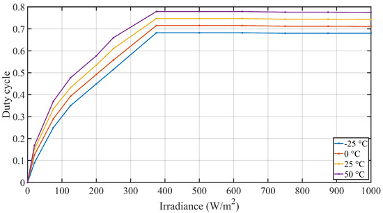
Figure 5.
Duty cycle of a three-leg interleaved boost converter connected to a 100 V DC bus vs solar panel (KC200GT) irradiance (W/m) for various ambient temperatures.
3. Experimental Fine-Tuning and Validation of the Electro-Thermal Model
In the previous section, the electro-thermal model of the three-leg interleaved boost converter model was constructed while mainly using the datasheets of the respective components together with a few assumptions to create and interconnect the thermal network. This section will determine the base error between the simulated and measured component case temperatures for the components within the examined boost converter for various combinations of ambient temperature and input power. A steady state temperature lookup table is obtained for each component by using the input power profile and the ambient temperature profile shown in Figure 6. The experimental setup used to validate the model is shown in Figure 7. A climate chamber varies the ambient temperature from 5 C to 65 C with a step of 10 C while a programmable voltage source controls the input power from 0 W to 195 W in steps of 15 W for every change in ambient temperature. Furthermore, a constant duty cycle of 0.3 is applied to the MOSFETs of the converter in order to prevent the input current from exceeding the maximum operating value of 10 A at the last step of the power profile. A switching frequency of 100 kHz was applied to the gates of the MOSFETs and a constant output resistance of 7.2 is used to dissipate the power. Both the input and output voltages as well as the currents are logged every minute in order to determine the power losses dissipated in the DC–DC converter for a total of 10 min per power step. The component case temperatures are simultaneously logged every minute using a FLIR X6580sc infrared camera with a resolution of 640 by 512 pixels in combination with an infrared window mounted in the door of the climate chamber. In order to remove the disparity in surface emissivity, the DC–DC converter has been coated with a thermographic paint that provides a uniform and temperature stable emissivity of 0.92 for each component case. Acquiring the actual component case temperatures will thus require only a single emissivity conversion for the entire PCB.
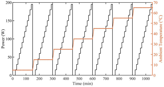
Figure 6.
The power (W) and ambient temperature (C) profile used as the input for the experimental validation of the electro-thermal DC–DC converter model.
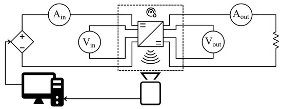
Figure 7.
Schematic of the experimental setup used to fine-tune and validate the electro-thermal DC–DC converter model.
The resulting average case temperatures for each component over the three legs of the interleaved boost converter are illustrated in Figure 8 after enduring the input profiles from Figure 6. It can be seen from Figure 8 that the diodes obtain the highest case temperatures throughout the experiment with a difference of 20 C in comparison with the rest of the components. This can be explained by the low duty cycle of 0.3 which requires the diodes to conduct double the amount of time in comparison to the MOSFETs. In addition, the required surface area for heat dissipation, which determines the thermal resistance of the diodes, is more limited in comparison with other components like the inductors.
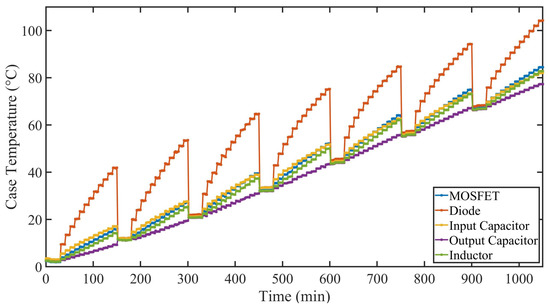
Figure 8.
Average measured component case temperatures (C) of the three-leg interleaved boost converter resulting from the input profile shown in Figure 6.
In order to validate the electro-thermal model using the case temperature profiles mentioned above, a fine-tuning of the convective heat transfer coefficient h in the simulation is required to emulate the forced air flowing through the climate chamber more accurately. A value of 40 W/m is adopted as it provides similar case temperatures from initial validation tests. The simulations have been performed for the power profiles of Figure 6 with ambient temperatures of 15 C, 35 C and 65 C in order to acquire an overall understanding of the maximum error between the simulated and the experimentally determined case component temperatures. A graphical representation of the thermal validation of the MOSFETs is depicted in Figure 9. In addition, the generated power losses in both the simulation and the experiment are shown in Figure 10 for an ambient temperature of 65 C. The maximum absolute errors for each component and ambient temperature at maximum converter input power are reported in Table 3. It would seem that the electro-thermal DC–DC converter model simulates an overall lower case temperature for each component with a maximum error of 3.03 C. This can be explained by looking at the increase in dissipated power in Figure 10 between the experiment and the simulation. The error will probably originate from the absence (or inaccurate datasheet value) of a parasitic resistance that was not considered in Section 2.1. The quadratic increase in the error supports this explanation by means of Joule’s law. However, localizing and adjusting this resistance value currently falls outside of the scope of the paper but this will be investigated in future work.
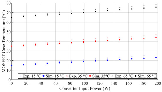
Figure 9.
The simulated and measured MOSFET case temperatures for various ambient temperatures.
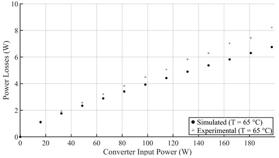
Figure 10.
The simulated and measured converter power losses for an ambient temperature of 65 C.
Table 3.
The maximum errors between the simulated and the measured component case temperatures of the three-leg interleaved boost converter for various ambient temperatures.
4. Constructing A FEM MOSFET Model
In the next section, the sensitivity of the electro-thermal DC–DC converter model to the temperature dependence of the electrical variables will be determined for reliability purposes. In order to evaluate the gain or loss in accuracy of a reliability analysis, a quantifiable output variable is required. Either the overall lifetime of a component can be estimated by analyzing the mission profile and using an empirical lifetime model [19] or a FEM model can be constructed in order to investigate the amount of plastic energy dissipated in the failure-prone parts of a component that is likely to fail according to past field studies [33]. In this case, the latter has been chosen due to providing more control over inputs such as the dimensions of the component and constitutive material models as well as the boundary conditions. According to literature, the active switching devices, being the MOSFETs, are more prone to failure than the other components when not using aluminum electrolytic capacitors in the design [34,35]. Specifically the bond wires and the die-attach are sensitive to the thermal stress generated by the discrepancy in coefficients of thermal expansion (CTE) of the different materials [36]. For this reason, a 2-D FEM model of the used MOSFET listed in Table 1 is constructed. X-ray imaging has been performed in order to determine the dimensions of the various material layers. The materials used in this MOSFET are a copper baseplate/heatsink, a solder die-attach, a silicon die, aluminum bond wires/leads and an epoxy resin with filler encapsulant soldered onto an PCB [37,38]. The constructed 2-D FEM model together with the X-ray images and a photograph of the used MOSFET are illustrated in Figure 11. The properties of the materials used in this model can be found in Table 4
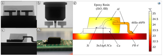
Figure 11.
(a–c) X-ray images and (d) a photograph of the MOSFET used in the interleaved boost converter together with (e) the temperature distribution of the constructed 2-D FEM model under an arbitrary load.
Table 4.
Properties of the materials used in the 2-D FEM MOSFET model of Figure 11 extracted from CES EduPack.
As mentioned in the previous paragraph, it is known that the bond wires and the die-attach of the MOSFET are the most prone to failure due to thermo-mechanical stress. The plastic behavior of the bond wires and the die-attach will be analyzed in steady state simulations with boundary conditions extracted from the electro-thermal DC–DC converter model. The three thermal boundary conditions used are the surrounding air determined by the chosen ambient temperature, the temperature of the middle of the PCB determined by the conductive heat transfer of the surrounding components and the heat losses in the die generated by the conduction losses and the switching losses of the MOSFET. The Johnson-Cook constitutive material model, shown in Equation (3), is used to simulate the plastic behavior of the used metals [39]. In this equation, is the equivalent stress, is the equivalent plastic strain, A is the yield stress of the material under reference conditions, B is the strain hardening constant, n is the strain hardening coefficient and C is the strain rate factor. Lastly, is the dimensionless strain rate and is the homologous temperature. The parameters used for every metal can be found in Table 5. A steady state surface plot of the plastic energy dissipation density inside the MOSFET is depicted in Figure 12 with boundary conditions extracted from the electro-thermal model using an input irradiance of 1000 W/m and an ambient temperature of 25 C. In this simulation, a maximum plastic energy dissipation density of 0.0974 J/cm is observed in the die-attach followed by 0.0636 J/cm in the heel of the bond wire. The steady state plastic energy dissipation density in the die-attach will therefore become the focus for quantifying the trade-offs in reliability for the sensitivity analyses of the next section.
Table 5.
Parameters used in the Johnson-Cook constitutive material model.
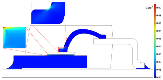
Figure 12.
Steady state plastic energy dissipation density plot (J/cm) of the constructed MOSFET FEM model resulting from a load of 1000 W/m on the solar panel at 25 C.
5. Sensitivity Analysis of the Electro-Thermal Model to the Temperature Dependent Electrical Variables
In this section, every temperature dependence of an electrical component included in the electro-thermal DC–DC converter model is evaluated in terms of change in the plastic deformation in the die-attach of the MOSFET, calculated with the aforementioned FEM model. The influence of not including a certain temperature dependence can be noticed by the MOSFET through a change in current which influences the losses generated in the junction, through a change in the surrounding temperature or through a combination of both. This will result in a change of the junction or case temperature of the MOSFET which will lead to an increase or decrease of thermal stress between the various material layers generated by the discrepancy in coefficients of thermal expansion (CTE). The irreversible part of this thermal stress, namely the plastic dissipation energy density, is then compared to the gain or loss in computation time for not including a certain temperature dependence in the electro-thermal model. In this topology, there is a lookup table for the temperature dependence of every inductance of the inductors, of every on-resistance of the MOSFETs or the diodes and of every forward voltage drop of the diodes. In addition, the temperature dependences of the capacitance and of all of the input capacitors are represented by two lookup tables. The same has been applied to the output capacitors. The final lookup table is used for the temperature dependence of the solar panel. A total of 17 lookup tables is evaluated for every switching period which increases the computation time significantly. Without the thermal capacitances, a simulation time of 1 s is required to reach the steady state. This takes 2 h of computation time when including all of the temperature dependences. The trade-off between computation time and plastic energy dissipation density for not including every temperature dependence separately is illustrated in Figure 13.
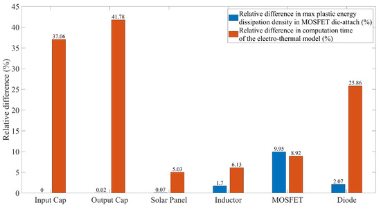
Figure 13.
The relative difference in maximum plastic energy dissipation density in the MOSFET die-attach (%) and computation time of the electro-thermal model (%) when excluding a certain temperature dependent electrical variable from the electro-thermal DC–DC converter model.
5.1. Capacitor
The variation in capacitance for either the input or the output capacitors used is determined by the type of dielectric. The X7R temperature stable dielectric provides a maximum capacitance variation of 15% over a temperature range of −55 C to 125 C. The temperature dependence of the equivalent series resistance on the other hand can be calculated using Equation (4) with the dissipation factor from the datasheet, the used switching frequency and the capacitance at a certain temperature provided by the properties of the dielectric mentioned before. It should be noted that only two lookup tables are used for the nine capacitors at the input and another two lookup tables are used for the seven capacitors at the output.
5.2. Photovoltaic Module
As mentioned in Section 2.4, the duty cycle of the three-leg interleaved boost converter varies with the ambient temperature endured by the photovoltaic module. This is caused by the temperature dependence of the open circuit voltage and the short circuit current of the panel which can be extracted from the respective datasheet. The difference in over the ambient temperature is negligible as the current remains constant. However, the difference of the over a temperature range of −25 C to 50 C results in an increase of the duty cycle with 10% which increases the conduction losses of the MOSFET.
5.3. Inductor
The temperature dependence of the inductance is often expressed in a negative correlation with the current passing through the inductor instead of its core temperature. This is implemented as such in the electro-thermal model with a decrease in inductance of 23% over 4.8 A as reported in the datasheet. The DC resistance of the inductor, consisting only of the wire losses, is implemented as the maximum value mentioned in the datasheet instead of the typical value. The reason is that there is a small difference between these two values, and also the low value of the temperature coefficient of the copper wire of per C.
5.4. MOSFET
The temperature dependence of the MOSFET affects both the conduction losses through the drain-source on-resistance and the switching losses. The exponential temperature dependent behavior can be extracted from the component’s datasheet in relation to the gate-source voltage that is being applied.
5.5. Diode
Both the forward voltage drop and the on-resistance of the diode vary with the temperature. The first will decrease with an increase in temperature which makes it easier for the diode to turn on while the last will increase with a rise in temperature. This means that at higher temperatures, the diode will generate less losses when conducting low currents because of the small forward voltage drop. However, at high currents, this effect is compensated and overtaken by the increase in on-resistance which makes the diode generate more losses than at lower temperatures. The temperature dependence of both variables can be extracted from the provided datasheets.
5.6. Discussion
In Figure 13, large discrepancies can be observed for the various temperature dependences in terms of the difference in plastic dissipation energy density in the die-attach of the MOSFET and the computation time of the electro-thermal model. The two largest decreases in computation time of 37.06% and 41.78% are produced by not including the temperature dependence of the input and output capacitors respectively. This does also not introduce any errors in the plastic energy dissipated in the MOSFET as the capacitors themselves do not generate a significant amount of heat because of the small input and output current ripple. Not including the temperature dependence of the solar panel, at an ambient temperature of 25 C, also does not induce a significant error. However, in a separate simulation this error rises towards 1% for an ambient temperature of 50 C which makes this a significant level of detail for cold or warm locations. A reduction in computation time of 5.03% was observed in both cases.
The temperature dependences that do introduce a significant error on the plastic energy dissipated in the MOSFET are, sorted by severity, the MOSFET itself with an error of 9.95%, the diode with an error of 2.07% and the inductor with an error of 1.7%. Not including the temperature dependence of the MOSFET itself will underestimate the losses generated in the die significantly because of the exponential temperature behavior of the drain-source on-resistance . The same reasoning can be applied to the diode and as a consequence less heat is transferred through the PCB and the surrounding air towards the MOSFET. Lastly, the temperature dependent change in inductance influences the current behavior and will therefore affect the losses generated in the MOSFET. In terms of computation time, not including the temperature dependence of the diode provides the largest reduction of 25.86% due to containing a lookup table for not only the on-resistance but also for the forward voltage . Not including the temperature dependence of the inductor will lead to a minor decrease in computation time of 6.13%. For the MOSFET, this reduction is 8.92% which is not considered a worthwhile trade-off due to the large error induced in the plastic dissipation energy density.
6. Conclusions
In this paper, the sensitivity of an electro-thermal model to the temperature dependence of the electrical variables was investigated. Firstly, an electro-thermal model of a three-leg interleaved boost converter for photovoltaic applications was constructed. Secondly, experimental testing was performed in order to fine-tune and validate this model. Thirdly, a 2-D FEM model of the MOSFET used in this converter was constructed based on X-Ray imaging results in order to calculate the plastic energy dissipation density in the failure-prone parts of the component. Finally, the trade-off for not including the temperature dependence of a certain electrical variable in the electro-thermal model on the plastic energy dissipation density in the die-attach of the MOSFET and the computation time of the electro-thermal model has been reported. The results indicated, on one hand, that the temperature dependence of the input capacitors, the output capacitors and the solar panel does not contribute to the plastic energy dissipated in the MOSFET while increasing the computation time significantly. On the other hand, the temperature dependence of the MOSFET, the diode and the inductor do generate a noticeable error. The best trade-off can be made by not including the temperature dependence of the diode as this would decrease the computation time by 25.86% while introducing an error of 2.07%. The temperature dependence of the MOSFET itself generates an error of 10% in plastic energy dissipation density and must therefore always be included in order to achieve accurate simulations. When taking these results into account, the computational efficiency of the electro-thermal modeling of DC–DC converters for reliability analyses can be improved significantly which will enable more iterations in the Design for Reliability methodology.
Author Contributions
Conceptualization, W.V.D.S. and M.D.; Data curation, S.R.; Funding acquisition, J.D. and M.D.; Methodology, W.V.D.S.; Software, W.V.D.S., S.R., O.A. and P.N.; Supervision, J.D. and M.D.; Validation, W.V.D.S. and S.R.; Visualization, P.N.; Writing—original draft, W.V.D.S.; Writing—review and editing, S.R., O.A. and M.D. All authors have read and agreed to the published version of the manuscript.
Funding
This research and the APC were funded by the project Rolling Solar, executed within the framework of the cross border collaboration program Interreg Euregio Meuse-Rhine V-A with financial support of the European Regional Development Fund.
Acknowledgments
The authors would like to thank the lab technicians of Hasselt University and KU Leuven for assisting with the experimental testing.
Conflicts of Interest
The authors declare no conflict of interest.
References
- International Energy Agency. 2019 Snapshot of Global PV Markets. Available online: https://www.researchgate.net/publication/332606669_2019_-_Snapshot_of_Global_Photovoltaic_Markets (accessed on 18 February 2020).
- Jäger-Waldau, A. PV Status Report 2019; Publications Office of the European Union: Brussels, Belgium, 2019. Available online: https://publications.jrc.ec.europa.eu/repository/handle/JRC118058 (accessed on 26 February 2020).
- The International Renewable Energy Agency. Renewable Energy Market Analysis: GCC 2019; International Renewable Energy Agency (IRENA): Abu Dhabi, UAE, 2019; Available online: https://www.irena.org/-/media/Files/IRENA/Agency/Publication/2019/Jan/IRENA_Market_Analysis_GCC_2019.pdf (accessed on 22 February 2020).
- The International Renewable Energy Agency. Renewable Power Generation Costs in 2017; International Renewable Energy Agency (IRENA): Abu Dhabi, UAE; Available online: https://www.irena.org/-/media/Files/IRENA/Agency/Publication/2019/Jan/IRENA_Market_Analysis_GCC_2019.pdf (accessed on 1 March 2020).
- Moore, L.; Post, H. Five years of operating experience at a large, utility-scale photovoltaic generating plant. Prog. Photovolt. Res. Appl. 2008, 16, 249–259. [Google Scholar] [CrossRef]
- Reigosa, P.D.; Wang, H.; Yang, Y.; Blaabjerg, F. Prediction of bond wire fatigue of IGBTs in a PV inverter under long-term operation. In Proceedings of the 2015 IEEE Applied Power Electronics Conference and Exposition (APEC), Charlotte, NC, USA, 15–19 March 2015; pp. 3052–3059. [Google Scholar] [CrossRef]
- Wang, N.; Cotton, I.; Evans, K. Impact of Thermal Cycling in Humid Environments on Power Electronic Modules. IEEE Trans. Compon. Packag. Manuf. Technol. 2012, 2, 1085–1091. [Google Scholar] [CrossRef]
- GopiReddy, L.; Tolbert, L.; Ozpineci, B. Power Cycle Testing of Power Switches: A Literature Survey. IEEE Trans. Power Electron. 2015, 30, 2465–2473. [Google Scholar] [CrossRef]
- Smet, V.; Forest, F.; Huselstein, J.; Richardeau, F.; Khatir, Z.; Lefebvre, S.; Berkani, M. Ageing and Failure Modes of IGBT Modules in High-Temperature Power Cycling. IEEE Trans. Ind. Electron. 2011, 58, 4931–4941. [Google Scholar] [CrossRef]
- Khazaka, R.; Mendizabal, L.; Henry, D.; Hanna, R. Survey of High-Temperature Reliability of Power Electronics Packaging Components. IEEE Trans. Power Electron. 2015, 30, 2456–2464. [Google Scholar] [CrossRef]
- Liu, Y. Power Electronic Packaging: Design, Assembly Process, Reliability, and Modeling; Springer: New York, NY, USA, 2012. [Google Scholar]
- Yang, S.; Xiang, D.; Bryant, A.; Mawby, P.; Ran, L.; Tavner, P. Condition Monitoring for Device Reliability in Power Electronic Converters: A Review. IEEE Trans. Power Electron. 2010, 25, 2734–2752. [Google Scholar] [CrossRef]
- Ye, X.; Chen, C.; Wang, Y.; Zhai, G.; Vachtsevanos, G.J. Online Condition Monitoring of Power MOSFET Gate Oxide Degradation Based on Miller Platform Voltage. IEEE Trans. Power Electron. 2017, 32, 4776–4784. [Google Scholar] [CrossRef]
- Kozak, J.P.; Ngo, K.D.; DeVoto, D.J.; Major, J.J. Impact of Accelerated Stress-Tests on SiC MOSFET Precursor Parameters. In Proceedings of the 2018 Second International Symposium on 3D Power Electronics Integration and Manufacturing (3D-PEIM), College Park, MD, USA, 25–27 June 2018; pp. 1–5. [Google Scholar] [CrossRef]
- Bormanis, O.; Ribickis, L. Accelerated Life Testing in Reliability Evaluation of Power Electronics Assemblies. In Proceedings of the 2018 IEEE 59th International Scientific Conference on Power and Electrical Engineering of Riga Technical University (RTUCON), Riga, Latvia, 12–13 November 2018; pp. 1–5. [Google Scholar] [CrossRef]
- Blaabjerg, F.; Zhou, D.; Sangwongwanich, A.; Wang, H. Design for reliability in renewable energy systems. In Proceedings of the 2017 International Symposium on Power Electronics (Ee), Novi Sad, Serbia, 19–21 October 2017; pp. 1–6. [Google Scholar] [CrossRef]
- Van De Sande, W.; Ravyts, S.; Sangwongwanich, A.; Manganiello, P.; Yang, Y.; Blaabjerg, F.; Driesen, J.; Daenen, M. A mission profile-based reliability analysis framework for photovoltaic DC-DC converters. Microelectron. Reliab. 2019, 100, 113383. [Google Scholar] [CrossRef]
- Ye, H.; Lin, M.; Basaran, C. Failure modes and FEM analysis of power electronic packaging. Finite Elem. Anal. Des. 2002, 38, 601–612. [Google Scholar] [CrossRef]
- Yang, Y.; Sangwongwanich, A.; Blaabjerg, F. Design for Reliability of Power Electronics for Grid-Connected Photovoltaic Systems. CPSS Trans. Power Electron. Appl. 2016, 1, 92–103. [Google Scholar] [CrossRef]
- Menozzi, R.; Cova, P.; Delmonte, N.; Giuliani, F.; Sozzi, G. Thermal and electro-thermal modeling of components and systems: A review of the research at the University of Parma. Facta Univ. Ser. Electron. Energetics 2015, 28, 325–344. [Google Scholar] [CrossRef]
- Shahjalal, M.; Lu, H.; Bailey, C. A review of the computer based simulation of electro-thermal design of power electronics devices. In Proceedings of the 20th International Workshop on Thermal Investigations of ICs and Systems, Greenwich, London, UK, 24–26 September 2014; pp. 1–6. [Google Scholar] [CrossRef]
- Albarbar, A.; Batunlu, C. Thermal Analysis of Power Electronics: Review. In Thermal Analysis of Power Electronic Devices Used in Renewable Energy Systems; Springer International Publishing: Cham, Switzerland, 2018; pp. 19–47. [Google Scholar] [CrossRef]
- Li, F.; Hao, R.; Lei, H.; Zhang, X.; You, X. The Influence of Parasitic Components on LLC Resonant Converter. Energies 2019, 12, 4305. [Google Scholar] [CrossRef]
- Rekioua, D.; Matagne, E. Optimization of Photovoltaic Power Systems: Modelization, Simulation and Control; Green Energy and Technology; Springer: London, UK; New York, NY, USA, 2012; OCLC: ocn756595412. [Google Scholar]
- Batunlu, C.; Musallam, M. 3D thermal model of power electronic conversion systems for wind energy applications. In Proceedings of the IEEE Global Humanitarian Technology Conference (GHTC), San Jose, CA, USA, 10–13 October 2014; pp. 369–376. [Google Scholar] [CrossRef]
- Infineon. Transient Thermal Measurements and Thermal Equivalent Circuit Models; Application Report AN 2015-10; Infineon Technologies AG: Neubiberg, Germany, 2018. [Google Scholar]
- Ravyts, S.; Vecchia, M.D.; Zwysen, J.; van den Broeck, G.; Driesen, J. Study on a cascaded DC-DC converter for use in building-integrated photovoltaics. In Proceedings of the 2018 IEEE Texas Power and Energy Conference (TPEC), College Station, TX, USA, 8–9 February 2018; pp. 1–6. [Google Scholar] [CrossRef]
- Künzi, R. Thermal design of power electronic circuits. In CERN Accelerator School: Power Converters; INSPIRE: Baden, Switzerland, 2014; pp. 311–327. [Google Scholar] [CrossRef]
- Texas Instruments. AN-1520 A Guide to Board Layout for Best Thermal Resistance for Exposed Packages; Application Report SNVA183B; Texas Instruments Incorporated: Dallas, TX, USA; Available online: http://www.ti.com/lit/an/snva183b/snva183b.pdf?ts=1591212046276 (accessed on 7 March 2020).
- Graovac, D.; Pürschel, M.; Kiep, A. MOSFET Power Losses Calculation Using the Data-Sheet Parameters. Available online: https://application-notes.digchip.com/070/70-41484.pdf (accessed on 10 March 2020).
- Texas Instruments. AN-2020 Thermal Design By Insight, Not Hindsight. Application Report SNVA419C. Available online: http://www.ti.com/lit/an/snva419c/snva419c.pdf?ts=1591212214437 (accessed on 17 March 2020).
- Rezk, H.; Eltamaly, A.M. A comprehensive comparison of different MPPT techniques for photovoltaic systems. Sol. Energy 2015, 112, 1–11. [Google Scholar] [CrossRef]
- Stoyanov, S.; Bailey, C.; Desmulliez, M. Optimisation modelling for thermal fatigue reliability of lead-free interconnects in fine-pitch flip-chip packaging. Solder. Surf. Mt. Technol. 2009, 21, 11–24. [Google Scholar] [CrossRef]
- Anderson, J.M.; Cox, R.W. On-line condition monitoring for MOSFET and IGBT switches in digitally controlled drives. In Proceedings of the 2011 IEEE Energy Conversion Congress and Exposition, Phoenix, AZ, USA, 17–22 September 2011; pp. 3920–3927. [Google Scholar] [CrossRef]
- Ruffilli, R.; Berkani, M.; Dupuy, P.; Lefebvre, S.; Weber, Y.; Legros, M. In-depth investigation of metallization aging in power MOSFETs. Microelectron. Reliab. 2015, 55, 1966–1970. [Google Scholar] [CrossRef][Green Version]
- Khong, B.; Legros, M.; Tounsi, P.; Dupuy, P.; Chauffleur, X.; Levade, C.; Vanderschaeve, G.; Scheid, E. Characterization and modelling of ageing failures on power MOSFET devices. Microelectron. Reliab. 2007, 47, 1735–1740. [Google Scholar] [CrossRef]
- Ruffilli, R.; Berkani, M.; Dupuy, P.; Lefebvre, S.; Weber, Y.; Warot-Fonrose, B.; Marcelot, C.; Legros, M. Aluminum metallization and wire bonding aging in power MOSFET modules. Mater. Today Proc. 2018, 5, 14641–14651. [Google Scholar] [CrossRef]
- Siow, K.S. (Ed.) Die-Attach Materials for High Temperature Applications in Microelectronics Packaging: Materials, Processes, Equipment, and Reliability; Springer International Publishing: Cham, Switzerland, 2019. [Google Scholar] [CrossRef]
- Li, T.; Zhao, B.; Lu, X.; Xu, H.; Zou, D. A Comparative Study on Johnson Cook, Modified Zerilli–Armstrong, and Arrhenius-Type Constitutive Models to Predict Compression Flow Behavior of SnSbCu Alloy. Materials 2019, 12, 1726. [Google Scholar] [CrossRef]
- Zein, H.; Irfan, O. Surface Roughness Investigation and Stress Modeling by Finite Element on Orthogonal Cutting of Copper. Metals 2018, 8, 418. [Google Scholar] [CrossRef]
- Qin, F.; An, T.; Chen, N. Strain rate effect and Johnson-Cook models of lead-free solder alloys. In Proceedings of the 2008 International Conference on Electronic Packaging Technology & High Density Packaging, Shanghai, China, 28–31 July 2008; pp. 1–7. [Google Scholar] [CrossRef]
- Bressan, J.D.; Lopez, K. New constitutive equation for plasticity in high speed torsion tests of metals. Int. J. Mater. Form. 2008, 1, 213–216. [Google Scholar] [CrossRef]


© 2020 by the authors. Licensee MDPI, Basel, Switzerland. This article is an open access article distributed under the terms and conditions of the Creative Commons Attribution (CC BY) license (http://creativecommons.org/licenses/by/4.0/).