Abstract
A novel interleaved high step-up DC-DC converter based on voltage multiplier cell and voltage-stacking techniques is proposed for the power conversion in renewable energy power systems. The circuit configuration incorporates an input-parallel output-series boost converter with coupled inductors, clamp circuits and a voltage multiplier cell stacking on the output side to extend the voltage gain. The converter achieves high voltage conversion ratio without working at extreme large duty ratio. The voltage stresses on the power switches are significantly lower than the output voltage. As a result, the low-voltage-rated metal-oxide-semiconductor field-effect transistors (MOSFETs) can be employed to reduce the conduction losses and higher conversion efficiency can be expected. The interleaved operation reduces the input current ripple. The leakage inductances of the coupled inductors act on mitigating the diode reverse recovery problem. The operating principle, steady-state analysis and design guidelines of the proposed converter are presented in detail. Finally, a 1-kW prototype with 28-V input and 380-V output voltages was implemented and tested. The experimental results are presented to validate the performance of the proposed converter.
1. Introduction
Nowadays, demand for clean or renewable energy sources has dramatically increased with population growth and the depletion of fossil fuel. Much effort has been made to explore renewable energy sources, such as photovoltaic (PV), fuel cell and wind energy systems [1,2,3]. The renewable energy grid-connected system with PV and fuel cells calls for high voltage-gain and high-efficiency dc-dc converters because the low voltage generated by the PV and fuel cells needs to be raised to a high voltage for the input of grid-connected inverter as shown in Figure 1. If the energy needs to be converted to a single-phase 220 V ac voltage utility grid, a 380–400 V dc bus voltage is required for the inverter. However, the outputs of PV and fuel cells are generally lower than 40 V [4] due to safety and reliability considerations in home applications. Thus, a front-end DC-DC converter with about ten times voltage gain is necessary to satisfy the requirement.

Figure 1.
Diagram of a renewable energy power system.
In order to achieve high voltage gain, a conventional boost converter or an interleaved boost converter can be employed with operating an extreme large duty ratio. However, it causes several problems of high switching losses, severe output diode reverse-recovery losses, and electromagnetic interference (EMI) [5]. Furthermore, for a high output-voltage converter, therefore, the high-voltage-rated MOSFETs and diode with large conduction resistance are necessary due to the voltage stresses on the power devices are equal to the output voltage. It will result in large conduction and switching losses. In practice, the voltage gain of boost converters is limited due to the parasitic parameters effect [5]. These problems are the main limitations of disadvantages for the boost converters.
In the literature, a lot of converter topologies have been proposed to obtain high step-up voltage gain [6,7,8,9,10,11,12,13,14,15,16,17,18,19,20,21,22]. For coupled inductor-based converters [6,7,8,9,10], the high voltage gain can be achieved by adjusting the turns ratio of the coupled inductor and duty ratio. However, the power loss and high voltage stress on the power switches occur owing to the leakage inductance of the coupled inductor. The switched-capacitor converters [11,12] can also obtain high voltage conversion ratio. However, many switches are required for these converters, and thus it leads to complexity of design for the driving circuit. The high step-up converters without a coupled inductor or transformer are proposed in [13,14]. Several kinds of interleaved high step-up converters with voltage multiplier cells have been proposed in [15,16,17,18,19]. The interleaved converters with three-winding coupled inductors are proposed to achieve high voltage conversion ratio and low input current ripple [20,21,22]. However, they are a little complex and difficult to design, which results in the circuit complexity and cost problems.
A novel interleaved high step-up converter based on voltage multiplier cell and voltage-stacking techniques is proposed herein for high voltage gain and high-power applications, as shown in Figure 2a. The topology utilizes the two-phase interleaved boost converter with parallel-input series-output connection and introduces dual clamp circuits and a voltage multiplier cell stacking on the output side to obtain the higher voltage conversion ratio. The converter has the following features:
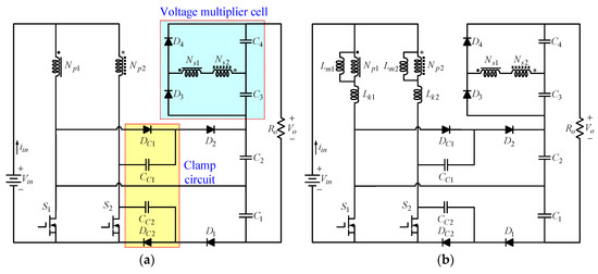
Figure 2.
Proposed converter and its equivalent circuit. (a) Proposed converter; (b) Equivalent circuit.
- (1)
- The converter has high step-up voltage gain without operating at extreme large duty ratio.
- (2)
- The voltage stress on the power switches is significantly lower than the output voltage. The low-voltage-rated MOSFETs with low on-resistances can thereby be adopted to reduce the conduction losses.
- (3)
- The diode reverse-recovery problem can be alleviated by the leakage inductances of the coupled inductors for most of the diodes.
- (4)
- Dual passive clamp circuits help to recycle the leakage energy of the coupled inductors and clamp the voltage stress of the power switches to a lower level.
- (5)
- The input current ripple, reduces is minimized due to the current ripple cancellation in the interleaved operation. Additionally, increases power level can be increased due to the current-sharing performance in high current applications.
This paper is organized as follows. The proposed converter and its operating principle are illustrated in Section 2. The steady-state analysis, design guidelines and performance comparison of the proposed converter are presented in Section 3. The experimental results on a 1000 W prototype circuit are provided to validate the performance of the proposed converter in Section 4. Finally, some conclusions are made in the last section.
2. Proposed Converter and Operating Principle
The proposed converter circuit is shown in Figure 2a, where and are the power switches, and are the clamp diodes, and are the clamp capacitors, and are the output diodes, and are the output capacitors, and are the switched diodes, and are the switched capacitors, and is the load. There are two coupled inductors in the proposed converter. The coupling references are marked by “” and “”. The circuit model of each coupled inductor includes an ideal transformer with the original turns ratio, which is in parallel with a magnetizing inductance and then in series with a leakage inductance. The equivalent circuit of the proposed converter is shown in Figure 2b, where and are the magnetizing inductance, and are the inductance, and are the primary and secondary windings of the coupled inductors, respectively, and the turns ratio of the coupled inductor is defined as . The dual passive clamp circuits are used to recycle the leakage energy and suppress the turn off voltage spikes on the power switches. The voltage multiplier cell is realized by the secondary windings of the coupled inductors with series connection, the switched diodes and the switched capacitors to increase the voltage gain.
In the operational analysis, the proposed converter operates in continuous conduction mode (CCM), and the gate signals of the power switches are interleaved with the same duty ratio greater than 0.5 and a phase shift. The key waveforms are shown in Figure 3. There are six operating modes in one switching period. The equivalent circuits for each mode are shown in Figure 4.
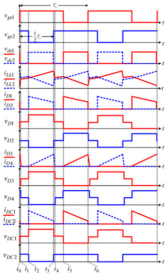
Figure 3.
Key waveforms of the proposed converter.
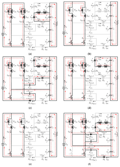
Figure 4.
Operating modes of the proposed converter. (a) Mode 1; (b) Mode 2; (c) Mode 3; (d) Mode 4; (e) Mode 5; (f) Mode 6.
Mode 1 []: At , the power switch is turned on, and the power switch remains in the turn-on state. The leakage current rises quickly and its increasing rate is limited by . The magnetizing inductance still transfers energy to the secondary side of the coupled inductors charging the switched capacitor . The diodes , , , and are reverse-biased, and only the switched diode is conducting as shown in Figure 4a. The current falling rate through the switched diode is controlled by the leakage inductances and , which alleviates the diode reverse recovery problem. This mode ends when the current through the diode decreases to zero at the instant , and the diode is turned off automatically. At the same time, the current through becomes equal to that of the magnetizing inductance .
Mode 2 []: During the time interval, both the switches and conduct, and all diodes are reverse-biased as depicted in Figure 4b. The magnetizing inductances and as well as the leakage inductances and are linearly charged by the input voltage . This mode ends at the instant , when the switch is turned off.
Mode 3 []: At , the switch is turned off, which makes the diodes and turn on due to the continuity of the leakage current . The switch remains in the turn-on state, as shown in Figure 4c. The energy kept by the magnetizing inductance is transferred not only to the secondary side of the coupled inductors but also to the output capacitor and the clamp capacitor . The current through decreases and flows through two paths. One path is through , , and , so that the clamp capacitor is discharged and the output capacitor is charged. The other path is through and , so that the clamp capacitor is charged. This mode ends when is turned on.
Mode 4 []: At , the power switch is turned on, and the power switch remains in the turn-on state. The diodes , , , and are reverse-biased, and only the switched diode is conducting as shown in Figure 4d. The current through the leakage inductance rises quickly, and the current through the leakage inductance falls quickly. The stored energy in the magnetizing inductance still transfers to the secondary side of the coupled inductors charging the switched capacitor . As the current through the leakage inductance increases, the secondary side current of the coupled inductors decreases. The of the current through the switched diode decreases and its falling rate controlled by the leakage inductances and , which alleviates the diode reverse recovery problem. This mode ends when the diode current decreases to zero at , and is turned off automatically. At the same time, the current through becomes equal to that of the magnetizing inductance .
Mode 5 []: The operating state of modes 5 and 2 are similar. During this interval, all diodes are turned off, as shown in Figure 4e. The magnetizing inductances and as well as the leakage inductances and are charged linearly by the input voltage . This mode is terminated as the switch is turned off.
Mode 6 []: The switch is turned off at , which turns on the diodes and . The switch remains in turn-on state. The current-flow path of this mode is shown in Figure 4f. The energy stored in the magnetizing inductance begins to transfer to the secondary side of the coupled inductors charging the switched capacitor via the switched diode . The current through the diode is controlled by the leakage inductances and . The leakage current decreases and flows to the clamp capacitor via and , meanwhile it flows to the output capacitor and the clamp capacitor via and . The time is the ending of a switching period when the power switch is turned on again.
3. Steady-State Analysis and Design Guidelines
In order to simplify the performance analysis of the proposed converter, the following assumptions are made.
- (1)
- Voltages on the capacitors are regarded as constant over one switching period due to their sufficiently large capacitances.
- (2)
- All of the power devices are ideal. The on-resistance and parasitic capacitances of the power switches are ignored, and the forward voltage drops of the diodes are neglected.
- (3)
- The leakage inductances of the couple inductors are much smaller than the magnetizing inductances, and, therefore, they are neglected.
- (4)
- The switching period is . The power switches operate with the same duty ratio D and out of phase.
3.1. Voltage Gain
Since the time intervals of modes 1 and 4 are very short, only modes 2, 3, 5 and 6 were considered for the steady-state analysis. Based on the operating principle discussed in the aforementioned section, the charging voltage of the magnetizing inductance is the input voltage during the switch is in the turn-on state for time , and the discharging voltage is the clamp voltage or minus the input voltage during the switch is in the turn-off state for time . By applying the voltage-second balance to the magnetizing inductance, the voltages on the clamp capacitors and can be calculated analogously to the output voltage of the conventional boost converter, which can be derived from
At modes 3 and 6, the voltages on the output capacitors and can be derived from Figure 4c,f, respectively. They can be expressed as
Moreover, the voltage on the switched capacitors and can also be derived from Figure 4c,f, respectively. The results are given by
From Figure 4b,e, it can be found that the output voltage is the sum of , , and . With the results of Equations (2)–(5), the output voltage can be derived from
Therefore, the voltage gain of the proposed converter is given by
Equation (7) confirms that the proposed converter has a high step-up voltage gain without adopting an extremely large duty ratio. The curve of the voltage gain related to the turns ratio of the coupled inductor and duty ratio is shown in Figure 5. As the turns ratio of the coupled inductors increases, the voltage gain is extended significantly. When the duty ratio is only 0.6, the voltage gain reaches 15 with the turns ratio .
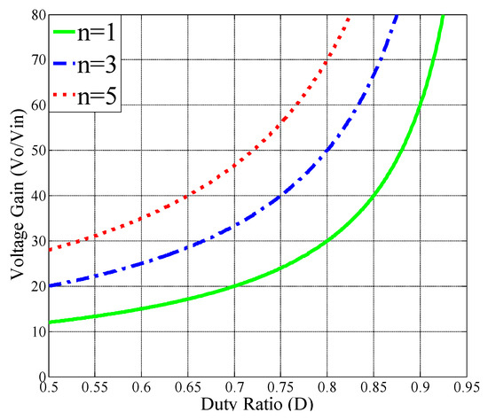
Figure 5.
Voltage gain of the proposed converter verse duty ratio for several turns ratio n.
3.2. Voltage Stresses on Semiconductor Devices
The voltage ripples on the capacitors are neglected to simplify the voltage stress analysis of the power switches and diodes. From Figure 4c,f, the power switch or is turned off and the drain-source voltages of and is equal to the voltages on the clamp capacitors and , respectively. Thus, the voltage stresses on the power switches and can be derived from
It can be seen that the switch voltage stress is greatly lower than the output voltage and it decreases greatly as the turns ratio of the coupled inductor increases. As a result, the low-voltage-rated MOSFETs with low on-resistance can be employed and the conversion efficiency can be improved.
From the operating modes of the proposed converter, the voltage stresses of the output diodes and are equal to the voltages and , respectively. The voltage stresses of the switched diodes and are the voltage plus the voltage . The voltage stresses of the output and switched diodes can be expressed as
At mode 3, the voltage stress of the clamp diode can be obtained as the sum of the voltages and . On the other hand, the voltage stress of the clamp diode is equal to the voltage from Figure 4f. Therefore, the voltage stresses of the clamp diodes can be given by
Equations (8)–(12) show that the proposed converter has the property of low voltage stresses on the semiconductor devices. The relationship between the normalized semiconductor-device voltage stresses and the turns ratio is depicted in Figure 6. It can be seen that the voltage stresses on , , , , and decreases as the turns ratio n increases. The voltage stress on and increases as the turns ratio n increases, but it is always lower than the output voltage. Therefore, the low-voltage-rated MOSFETs with low on-resistance and Schottky diode without reverse-recovery time can be used to improve the efficiency.
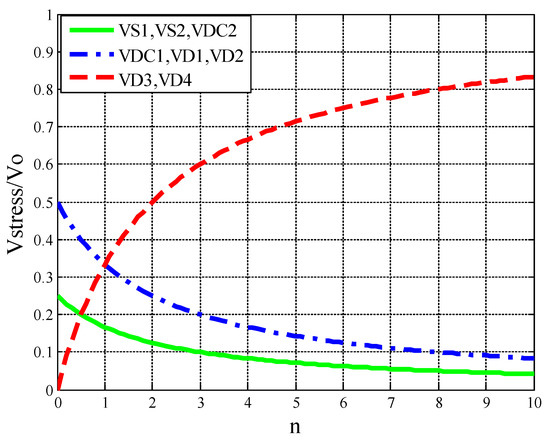
Figure 6.
Normalized semiconductor-device voltage stresses versus turns ratio n.
3.3. Design Guidelines
3.3.1. Turns Ratio Design
The voltage gain expression is given in Equations (7). A proper turns ratio n can be obtained once the voltage gain is assigned and the duty ratio D is designed, which is given by
3.3.2. Power Switches and Diodes Selection
According to Equations (8)–(12), the voltage stresses of the semiconductor devices are obtained, which can be employed to select the power devices. In practice, voltage spikes may occur during the switching transition process due to the effect of the leakage inductance and parasitic capacitor. Therefore, a reasonable margin of safety is necessary for the voltage rating of the selected power devices.
3.3.3. Coupled Inductor Design
A good criterion for designing the magnetizing inductance is to maintain the continuous-conduction mode (CCM) and set an acceptable current ripple in the magnetizing inductance of the coupled inductor. Assume that the coupled inductors have the same magnetizing inductance, that is . The magnetizing inductance current ripple can be expressed as
The average magnetizing current is given by
For the CCM operation of the proposed converter, the following condition holds
Substituting Equations (14) and (15) into Equation (16), the magnetizing inductance can be determined for the CCM operation, which is given by
where is the switching frequency and is the load.
3.3.4. Capacitor Design
In the preceding analysis, the capacitors are assumed to be very large to keep their voltages constant. In practice, the voltages cannot be kept constant with a finite capacitance. An acceptable voltage ripple is the main consideration in designing the capacitors. The relationship of the voltage ripple and the capacitance is given by
where is the change in charge or discharge, and is the voltage ripple on the capacitor C.
The output capacitor is discharged by the load current during modes 2, 3 and 5. The total time is equal to . Therefore, the voltage ripple can be obtained as
Substituting Equation (3) into Equation (19), it can be expressed by the following equation.
It is useful to rearrange the equation to express required capacitance in terms of specified voltage ripple for the output capacitor , which is given by
Similarly, the output capacitor , switched capacitors and , and clamp capacitors can be derived to express required capacitance in terms of specified voltage ripple, which are given by
where , , , and are the tolerant voltage ripples on the capacitors , , , and , respectively.
3.4. Performance Comparison
The performance comparison between the converters published in [20,21,22] and the proposed converter is shown in Table 1. The relationship between the voltage gain and the duty ratio in these converters with the turns ratio n = 1.5 is shown in Figure 7. It can be seen that the voltage gain of the proposed converter is higher than the other converters. In fact, if the turns ratio n of the coupled inductor is designed by less than 3, then the voltage gain of the proposed converter is the highest. Moreover, the voltage stress on the switches and the highest voltage stress on diodes of the proposed converter are the lowest among the compared converters. The component number of the proposed converter is less than that of the converter published in [21]. Clearly, the proposed converter is suitable for the high step-up and high voltage applications.

Table 1.
Converter performance comparison.
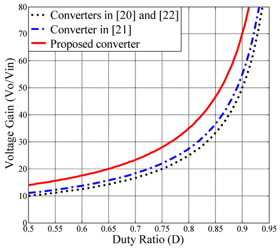
Figure 7.
Voltage gains versus duty ratio with turns ratio n = 1.5.
4. Experimental Verifications
To validate the performance and effectiveness of the proposed converter, a 1000 W laboratory prototype with 28-V input and 380-V output voltages was built and tested with the specifications and parameters shown in Table 2. The experimental results shown in the Figure 8, Figure 9, Figure 10, Figure 11, Figure 12, Figure 13, Figure 14 and Figure 15 are measured under full-load conditions 1000 W.

Table 2.
Components and parameters of the prototype.
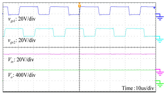
Figure 8.
Measured waveforms of the gating signals and the input and output voltages.
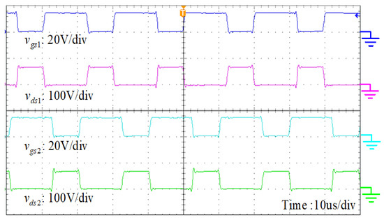
Figure 9.
Measured waveforms of the gating signals and the drain-source voltages of power switches.
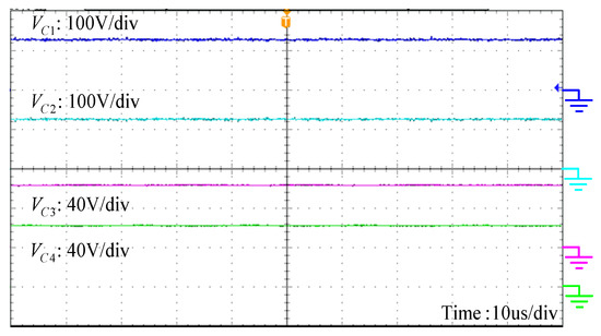
Figure 10.
Measured waveforms of the voltages on the switched capacitors and the output capacitors.
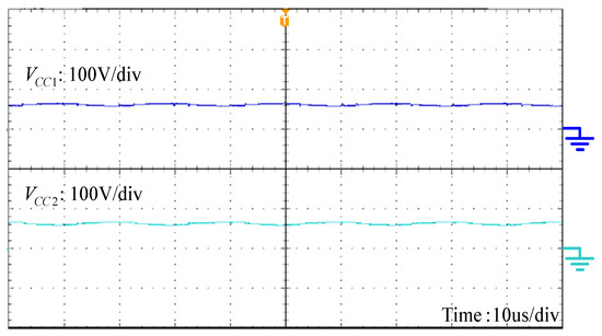
Figure 11.
Measured waveforms of the voltages on the clamp capacitors.
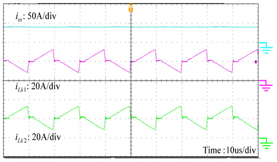
Figure 12.
Measured waveforms of the input current and the currents through the leakage inductances.
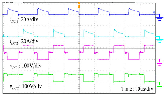
Figure 13.
Measured waveforms of the voltages and currents on the clamp diodes.
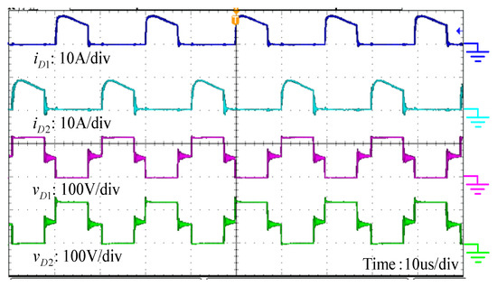
Figure 14.
Measured waveforms of the voltages and currents on the output diodes.
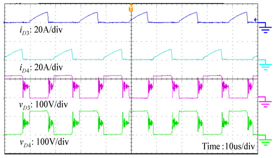
Figure 15.
Measured waveforms of the voltages and currents on the switched diodes.
Figure 8 shows t waveforms of the interleaved PWM signals and , the input voltage = 28 V and the output voltage = 380 V. The duty ratio is about 0.58. Thus, the high step-up voltage gain is realized without operating at an extremely large duty ratio. The waveforms of gate signals and the drain-source voltages and are shown in Figure 9. It can be seen that the voltage stresses on the power switches are about 63 V, which is only one-sixth of the output voltage. Thus, one can adopt low-voltage-rated devices to reduce the conduction and switching losses.
Figure 10 depicts the waveform of the voltages on the output capacitors and the switched capacitors. Because the turns ratio n is equal to one, the voltages and are half of and . The experimental results are in a good agreement with the theoretical analysis given in Equations (2)–(5). Figure 11 shows the voltages on the clamp capacitors. It can be seen that the voltage ripple is small, which can clamp the voltage stress of the power switches. Figure 12 shows the waveforms of the input current and the currents through the leakage inductances. As can be seen, the currents through the leakage inductances are interleaved such that the input current ripple is very small. The average current of is quite similar to , which is a half of the input current. Thus, the current sharing performance is good due to the symmetrical interleaved structure.
Figure 13, Figure 14 and Figure 15 depict the voltage and current waveforms on the clamp diodes, output diodes and switched diodes, respectively. One can see that the reverse recovery currents are very small because the current falling rates are controlled by the leakage inductances. As a result, the reverse recovery losses are alleviated. The voltage stress on the clamp diode is half of that on clamp diode , which is consistent with the theoretical analysis in Equations (11) and (12). The voltage stress on output diodes and switched diodes – are almost identical to the turns ratio n of one, which is in agreement well with the theoretical analysis in Equations (9) and (10). The overvoltage and ringing on the diodes and are larger than to the other diodes, as shown in Figure 15. This is a result of the simplified equivalent circuit with the leakage inductance introduced only on the primary side such that the clamp circuits are ineffective, to limit the overvoltage on and . Furthermore, the voltage stresses of all the diodes are much lower than the output voltage.
In order to obtain a regulated and constant output voltage in spite of input voltage variation and output load disturbance, the closed-loop control with type III compensator is implemented [23]. There are three poles (one at the origin) and two zeros provided by this compensation. The experimental result under the step load change from half load 500 W to full load 1000 W and vice versa is illustrated in Figure 16. It can be seen that the transient voltage ripple of the output voltage is small and insensitive to the load change. This means that the compensator design can deliver a dynamic performance. The experimental conversion efficiency of the presented converter is given in Figure 17, which is measured by the power analyzer (HIOKI 3390). The full-load efficiency is about 86% and the peak value of efficiency is 94.5% obtained at the output power of 200 W.
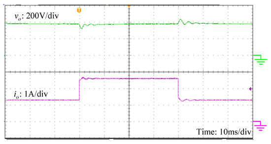
Figure 16.
Output voltage response with step load change.
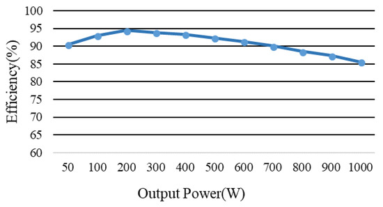
Figure 17.
Experimental conversion efficiency of the implemented converter.
5. Conclusions
A new interleaved high step-up DC-DC converter based on voltage multiplier cell and voltage-stacking technique is proposed. The high step-up voltage conversion can be achieved without working at extremely large duty ratio. The switch voltage stress is much lower than the output voltage such that the low-voltage-rated power devices with low on-resistance can be adopted to reduce the conduction losses. Dual passive clamp circuits help to recycle the leakage energy of the coupled inductors and clamp the voltage stress of the switches to a lower level. The interleaved operation reduces the input current ripple. The diode reverse-recovery problem is alleviated by the leakage inductances of the coupled inductors for most of the diodes. The operating principle, the steady-state analysis and design guidelines of the proposed converter are presented. Finally, a 1000 W prototype converter was built and tested to validate the converter’s performance.
Author Contributions
S.-J.C. and S.-P.Y. conceived and designed the converter circuit. M.-J.S. performed the experiments. C.-M.H. and H.-M.C. analyzed the performance. S.-J.C. wrote the manuscript.
Funding
The authors gratefully acknowledge financial support from the Ministry of Science and Technology, Taiwan, under the grant number MOST 106-2632-E-168-001.
Conflicts of Interest
The authors declare that there is no conflict of interest.
References
- Yang, B.; Li, W.; Zhao, Y.; He, X. Design and analysis of a grid connected PV power system. IEEE Trans. Power Electron. 2010, 25, 992–1000. [Google Scholar] [CrossRef]
- Carrasco, J.M.; Franquelo, L.G.; Bialasiewicz, J.T.; Galvan, E.; Guisado, R.C.P.; Prats, M.A.M.; Leon, J.I.; Moreno-Alfonso, N. Power-electronic systems for the grid integration of renewable energy sources: A survey. IEEE Trans. Ind. Electron. 2006, 53, 1002–1016. [Google Scholar] [CrossRef]
- Arunkumari, T.; Indragandhi, V. An overview of high voltage conversion ratio dc-dc converter configurations used in DC micro-grid architectures. Renew. Sustain. Energy Rev. 2017, 77, 670–687. [Google Scholar] [CrossRef]
- Ajami, A.; Ardi, H.; Farakhor, A. A novel high step-up DC-DC converter based on integrating coupled inductor and switched-capacitor techniques for renewable energy applications. IEEE Trans. Power Electron. 2015, 30, 4255–4263. [Google Scholar] [CrossRef]
- Tofoli, F.L.; Pereira, D.C.; Paula, W.J.; Junior, D.S.O. Survey on non-isolated high-voltage step-up DC–DC topologies based on the boost converter. IET Power Electron. 2015, 8, 2044–2057. [Google Scholar] [CrossRef]
- Hsieh, Y.P.; Chen, J.F.; Liang, T.J.; Yang, L.S. Novel high step-up dc-dc converter with coupled-inductor and switched-capacitor techniques for a sustainable energy system. IEEE Trans. Power Electron. 2011, 26, 3481–3490. [Google Scholar] [CrossRef]
- Honarjoo, B.; Madani, S.M.; Niroomand, M.; Adib, E. Analysis and Implementation of a New Single Switch, High Voltage Gain DC-DC Converter with a Wide CCM Operation Range and Reduced Components Voltage Stress. J. Power Electron. 2018, 18, 11–22. [Google Scholar]
- Hu, X.; Gong, C. A high voltage gain DC-DC converter integrating coupled-inductor and diode-capacitor techniques. IEEE Trans. Power Electron. 2014, 29, 789–800. [Google Scholar]
- Liu, H.; Ai, J.; Li, F. A novel high step-up converter with a switched-coupled-inductor-capacitor structure for sustainable energy systems. J. Power Electron. 2016, 16, 436–446. [Google Scholar] [CrossRef]
- Wong, Y.S.; Chen, J.F.; Liu, K.B.; Hsieh, Y.P. A novel high step-up DC-DC converter with coupled inductor and switched clamp capacitor techniques for photovoltaic systems. Energies 2017, 10, 378. [Google Scholar] [CrossRef]
- Wei, C.L.; Shih, M.H. Design of a switched-capacitor DC-DC converter with a wide input voltage range. IEEE Trans. Circuits Syst. 2013, 60, 1648–1656. [Google Scholar] [CrossRef]
- Chung, H.S.; Ioinovici, A.; Cheung, W.L. Generalized structure of bi-directional switched-capacitor dc/dc converters. IEEE Trans. Circuits Syst. I 2003, 50, 743–753. [Google Scholar] [CrossRef]
- Yang, L.S.; Liang, T.J.; Chen, J.F. Transformerless DC-DC Converters with high step-up voltage gain. IEEE Trans. Ind. Electron. 2009, 56, 3144–3152. [Google Scholar] [CrossRef]
- Pan, C.T.; Chuang, C.F.; Chu, C.C. A Novel transformer-less adaptable voltage quadrupler dc converter with low switch voltage stress. IEEE Trans. Power Electron. 2014, 29, 4787–4796. [Google Scholar] [CrossRef]
- Tseng, K.C.; Chen, C.T.; Cheng, C.A. A high-efficiency high step-up interleaved converter with a voltage multiplier for electric vehicle power management applications. J. Power Electron. 2016, 16, 414–424. [Google Scholar] [CrossRef]
- Prudente, M.R.; Pfitscher, L.L.; Emmendoerfer, G.; Romaneli, E.F.; Gules, R. Voltage multiplier cells applied to non-isolated converters. IEEE Trans. Power Electron. 2008, 23, 871–887. [Google Scholar] [CrossRef]
- Li, W.; Zhao, Y.; Deng, Y.; He, X. Interleaved converter with voltage multiplier cell for high step-up and high efficiency conversion. IEEE Trans. Power Electron. 2010, 25, 2397–2408. [Google Scholar] [CrossRef]
- Tseng, K.C.; Huang, C.C. High step-up high-efficiency interleaved converter with voltage multiplier module for renewable energy system. IEEE Trans. Ind. Electron. 2014, 61, 1311–1319. [Google Scholar] [CrossRef]
- Shen, C.L.; Chiu, P.C.; Lee, Y.C. Novel interleaved converter with extra-high voltage gain to process low-voltage renewable-energy generation. Energies 2016, 9, 871–882. [Google Scholar] [CrossRef]
- Li, W.; Zhao, Y.; Wu, J.; He, X. Interleaved high step-up converter with winding-cross-coupled inductors and voltage multiplier cells. IEEE Trans. Power Electron. 2012, 27, 133–143. [Google Scholar] [CrossRef]
- Nouri, T.; Hosseini, S.H.; Babaei, E.; Ebrahimi, J. Interleaved high step-up DC-DC converter based on three-winding high-frequency coupled inductor and voltage multiplier cell. IET Power Electron. 2015, 8, 175–189. [Google Scholar] [CrossRef]
- He, L.; Liao, Y. An advanced current-autobalance high step-up converter with a multicoupled inductor and voltage multiplier for a renewable power generation system. IEEE Trans. Power Electron. 2016, 31, 6992–7005. [Google Scholar]
- Cao, L. Type III compensator design for power converters. Power Electron. Technol. 2011, 1, 20–25. [Google Scholar]
© 2018 by the authors. Licensee MDPI, Basel, Switzerland. This article is an open access article distributed under the terms and conditions of the Creative Commons Attribution (CC BY) license (http://creativecommons.org/licenses/by/4.0/).