Abstract
This paper presents a low-power fully integrated quadrature signal generator for system-on-chip (SoC) impedance spectroscopy applications. It has been designed in a 0.18 μm-1.8 V CMOS technology as a self-contained oscillator, without the need for an external reference clock. The frequency can be digitally tuned from 10 to 345 kHz with 12-bit accuracy and a relative mean error below 1.7%, thus supporting a wide range of impedance sensing applications. The proposal is experimentally validated in two impedance spectrometry examples, achieving good magnitude and phase recovery results compared to the results obtained using a commercial LCR-meter. Besides the wide frequency tuning range, the proposed programmable oscillator features a total power consumption lower than 0.77 mW and an active area of 0.129 mm2, thus constituting a highly suitable choice as stimulation module for instrument-on-a-chip devices.
1. Introduction
Recent advances in microsensing techniques are leading to a growing need for on-chip electronic instrumentation, not only providing the required performances but also simultaneously complying with the constraints of low power and compact size, to fully satisfy the emerging market demands and potential applications of portable and wearable sensing devices. New transduction techniques in micro-integrated sensors include resonant detection and complex impedance characterization, as in surface acoustic wave sensors [1], gas sensors [2,3,4,5], laser interferometry [6], brain monitoring [7], non-invasive light detection [8] or biological impedance measurement [9,10]. For these transducers, a suitable interrogation approach, which presents advantages compared to other electronic readout techniques due to its characteristics, is synchronous demodulation.
Synchronous demodulation [11,12] can be implemented in CMOS technology [13,14] using phase sensitive detection (PSD) or quadrature modulators, which extract the signal amplitude and phase information at a specific frequency while noise signals at other frequencies are rejected. Figure 1 illustrates the conceptual scheme of a dual PSD module. A device sensor is excited by an input signal , providing an output that is next multiplied by two 90 degrees shifted reference signals also with frequency . The resulting mixer outputs are finally low-pass filtered, obtaining two DC values and , proportional to the processed signal:
so that the magnitude and phase, or equivalently, the real and imaginary part of the sensor impedance can be obtained.
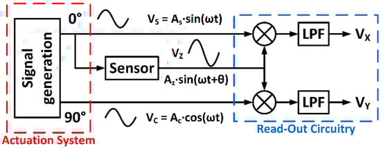
Figure 1.
Conceptual scheme of the phase sensitive detection (PSD) technique.
Accordingly, in dual PSD-based conditioning electronics, the stimulation system requires the generation of two 90 degrees shifted signals and , so that one of them is also used as the sensor excitation. Most of microelectronic implementations of synchronous demodulators integrate the read-out circuit together with the transducer in the same chip, but leave the stimulation system out of the integrated circuit, using external signal generators, thus increasing size, power consumption and complexity.
Therefore, a fully integrated PSD instrument will require the design of a self-contained suitable integrated stimulation system. This paper presents the implementation and experimental results of a versatile CMOS signal generation circuit suitable for portable PSD applications. Preliminary simulation results have been previously presented in [15]. To be self-contained, it is based on a digitally programmable analog quadrature sinusoidal oscillator. It generates two sinusoidal signals in quadrature, whose frequency is digitally controlled by a 12-bit custom digital-to-analog (DAC) architecture over a wide range up to hundreds of kHz, covering most typical impedance sensor operation. It has been fabricated in a 0.18 µm-1.8 V CMOS technology, featuring low-power and compact size, to be suitable for applications in portable on-chip systems, and it has been experimentally characterized as stimulation block in two impedance spectroscopy (IS) applications, from structural characterization to bio-impedance measurement.
The paper is organized as follows. Section 2 describes the proposed stimulation system, explaining its basic blocks and its implementation. Section 3 summarizes the experimental results of the fabricated prototype. Section 4 presents the experimental results for two IS applications. Finally, conclusions are drawn in Section 5.
2. Quadrature Oscillator
The proposed quadrature sinusoidal oscillator is based on an analog core implementation. It provides low-voltage low-power compatibility with a CMOS hardware efficient architecture. To achieve a precise trimming over a wide frequency range, this architecture incorporates custom digitally programmable blocks, so that can be easily adjusted according to the target application. The oscillator topology is shown in Figure 2. It is based on a single supply active-RC two integrator loop using three operational amplifiers (OpAmps) as active cells, two capacitors and six resistances: resistors , and are passive, while are identical active resistors, respectively conformed by a passive resistor in series with a digital control cell based on a current summing/division network (CS/DNs) [15].
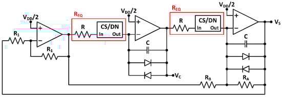
Figure 2.
Proposed programmable quadrature oscillator topology.
This oscillator generates a quadrature signal pair (, ) with a phase shift of 90° [15]. By direct analysis of the first integrator loop, the relation between signals and is
Analogously, analyzing the second integrator loop,
Hence, from (2) and (3), the characteristic equation of the system is
Thus, the oscillation condition is given by
and the oscillation frequency is
so that both characteristics are independently controllable. In practice, must be slightly higher than to guarantee oscillation. Combining (2) and (6), it is straightforward that resistors must vary simultaneously to keep constant the output amplitude ratio for the two output quadrature signals
2.1. Active Cells Design
2.1.1. Operational Amplifier
A two-stage OpAmp (Figure 3) has been specifically designed to accomplish high gain, high unity gain frequency, and class AB output to enhance the driving capability with optimum power consumption. The input stage is a folded cascode operational transconductance amplifier (OTA), which develops high gain with a simple single-stage topology, thus being suitable for low-voltage operation. The output is a class AB push-pull buffer. This additional stage provides rail-to-rail operation, while adds extra gain to the OpAmp. Stability is guaranteed through classical Miller compensation. The main post-layout simulated performances for a 1.8 V-0.18 µm CMOS implementation are summarized in Figure 3.
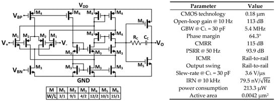
Figure 3.
Operational amplifier schematic topology with transistor sizes in µm, and main post-layout simulated performances.
2.1.2. Current Summing/Division Network
The digitally programmable block is based on a current summing/division network (CS/DN) approach [15], that digitally controls the current to be delivered to the virtual ground node of single-OpAmp trans-impedance amplifiers, setting a linear programmable gain in the case of resistive feedback, or a linear programmable time constant in the case of capacitive feedback. The CS/DN scheme is shown in Figure 4.
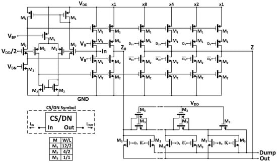
Figure 4.
CS/DN schematic topology and transistor sizes in µm.
A bit resolution has been chosen to attain a good tradeoff between tuning range, resolution, power and area consumption. The CSN provides the most significant bits (MSB). It is basically a wide-swing class AB second generation current conveyor (CCII+) topology, where terminal X is the input CS/DN current terminal. The input common mode voltage is fixed by setting terminal Y to .
The Z output stage () is replicated to achieve 16 identical unity gain currents (15 Z branches and Z0 branch, Figure 5). So, Z is directly decoded to a binary representation by driving the gates of the corresponding cascode output transistors to attain currents ×1, ×2, ×4, ×8 with bits to , respectively. The Z0 unitary current is the input current of the least significant bit (LSB) segment: a MOS R/2-R ladder implemented with NMOS transistors of identical size. The last branch of the ladder is connected to the Dump node, and therefore there is no offset current for the zero digital input. Classical MOS ladders are the best solution in terms of size and power consumption for resolutions up to 8 bit, which can be increased up to 10 bit with careful layout techniques at the cost of area [16]. Hence, the resolution of each segment of the CS/DN was set to keep a good tradeoff between circuit performance, complexity and power consumption.
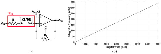
Figure 5.
(a) Active-RC integrator built around the proposed OpAmp and CS/DN; and (b) simulated integrator characteristic frequency.
Therefore, the full-scale current is
and the LSB current is
Thus, the total output analog current is given by
where are the coefficients of the 12-bit digital control word representing the input binary code. Hence, a linear relationship is obtained between the digital programming word and the output current.
Note that the Dump node of the MOS ladder (Figure 4) must be connected to a virtual ground to preserve the output terminals symmetry, ensuring a right current division.
This 12 bit CS/DN structure has been implemented in a 1.8 V-0.18 µm CMOS process, with the transistor sizes and parameter values indicated in Figure 4. It features as main post-layout performances: 12-bit resolution with linearity errors below ±0.5 LSB, static power consumption lower than 44 µW, an intrinsic bandwidth of 6 MHz and an active area of 0.0085 mm2.
The cell behavior has been tested in a first order analog integrator (Figure 5a), using the OpAmp shown in Figure 3 as active component. When this module is connected in series with a linear resistor as shown in Figure 5a, the input current to the programmable module is , generating a current at the output given by (7) which is transferred to the integrator feedback impedance (). The voltage transfer function for is
and the combined R-CS/DN module behaves as a programmable resistor, with an equivalent resistance
Thus, the transfer function of an ideal integrator is recovered, but exhibiting a non-inverting behavior due to the 180° phase shift introduced in the current follower (, ) of the CCII+ in the CS/DN. The integrator characteristic frequency is given by
showing a linear relationship with the 12-bit digital control word. Theoretical frequency range varies from to in steps of . Figure 5b shows the simulated integrator characteristic frequency over the whole digital range, setting kΩ, MΩ and pF, to attain a theoretical frequency range from 0 to 339.5 kHz, with a resolution of 82.9 Hz. Maximum relative error of the integrator characteristic frequency is below 0.7%.
Therefore, in active-RC systems, with characteristic frequencies given by ~1/RC, this cell brings out an accurate frequency trimming with linear dependence on the digital input code.
2.2. Quadrature Oscillator Design
To attain a fully integrated 1.8 V-0.18 µm CMOS stimulation system operating up to hundreds of kHz, the passive components are set to the values shown in Table 1. Resistors are implemented with a high resistive polysilicon (HRP) layer and capacitive elements are metal-insulator-metal (MIM) capacitors. Floating diodes in the integrator loops are standard cells provided by the CMOS technology, built in a P-well, each having µm size. They are used to avoid saturation of the output signal amplitudes [17].

Table 1.
Oscillator design parameters.
Figure 6 shows a microphotograph of the fabricated prototype. Its silicon area is 0.129 mm2, of which about 70% corresponds to the capacitors.
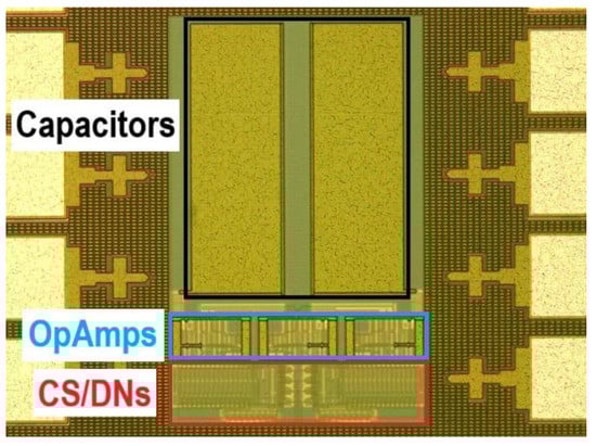
Figure 6.
Quadrature oscillator prototype (active area: 283 µm × 455 µm).
3. Experimental Performances
3.1. Test Setup
Figure 7 shows the block diagram of the experimental setup used to test the fabricated quadrature oscillator. A Keysight E3611A power supply (Keysight Technologies, Santa Rosa, CA, USA) provides the 1.8 V supply voltage required by the circuit. Frequency programming is provided by a NI USB-6009 Data Acquisition Card (National Instruments, Austin, TX, USA) that controls the 12-bit registers in the device. A Keithley 2602A two-channel SourceMeter Unit (Keithley Instruments Inc., Cleveland, OH, USA) sets both the Out and Dump node voltages to a virtual ground value (0.9 V), while the oscillator dynamic characteristics are registered through a Tektronix 4104 Digital Phospor Oscilloscope (Tektronix Inc., Cleveland, OH, USA). A Keysight 53132A Universal Counter (Keysight Technologies, Santa Rosa, CA, USA) accurately measures the oscillation frequency. Characterization system is controlled by a computer using Universal Serial Bus (USB) and General Purpose Interface Bus (GPIB) communication standards. Figure 8 shows some photographs of the experimental measurement setup.
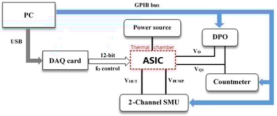
Figure 7.
Experimental setup block diagram.
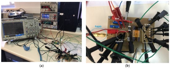
Figure 8.
Experimental setup: (a) General view of the instrumentation used; and (b) A detail of the ASIC connected to the circuit board, indicating the supply and bias lines, the output signals, and the 12 bit digital input.
3.2. Experimental Results
Figure 9a shows the oscillation frequency measured as a function of the 12-bit digital control. Effective frequency ranges from 10 kHz for a digital value of #80 to 345 kHz for a register value of #FFF, with a maximum relative error below 4% and absolute mean error lower than 1.7% (Figure 9b). Frequency peak errors are due to activation/deactivation of the most significant bits (associated to the CCII+) in the programmable cell, resulting in changes in the input/output impedance of the CS/DN block. Figure 9c shows the phase error for the quadrature output signals, which remains lower than 2% with an absolute mean error below 0.84%.
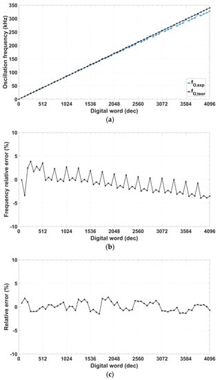
Figure 9.
Oscillator dynamic performance measurements: (a) Oscillation frequency; (b) Frequency relative error; (c) Phase relative error.
Common mode voltage (Figure 10) remains constant to (0.9 V) for the whole digital range with an error below 0.4%, while peak-to-peak voltage varies from 1.32 to 1.52 V with the digital control code for signal and from 1.28 to 1.50 V for signal . Maximum difference between them is 0.027 V (~2% deviation). Due to the CS/DN architecture, the power consumption is code-dependent, being always lower than 770 µW (Figure 11).
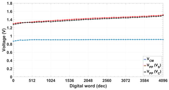
Figure 10.
Oscillator common mode (VCM) and peak-to-peak (VPP) voltage of quadrature signals.
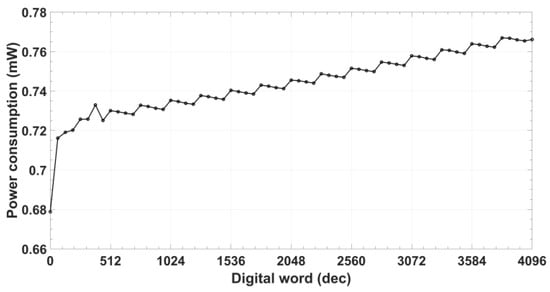
Figure 11.
Oscillator power consumption.
Figure 12a shows an oscilloscope screenshot of the output quadrature signals for the digital word #500, and Figure 12b shows its spectral analysis, using a Hanning window. These signals oscillate at a frequency of 114.3 kHz, with a total harmonic distortion (THD) of −36 dB. Figure 12c shows the THD value along the digital range. Finally, Table 2 summarizes the main performances of the fabricated oscillator.
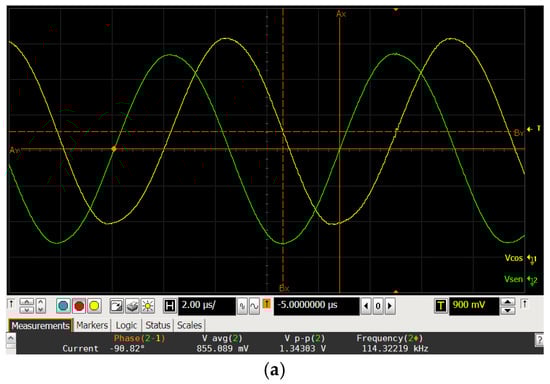
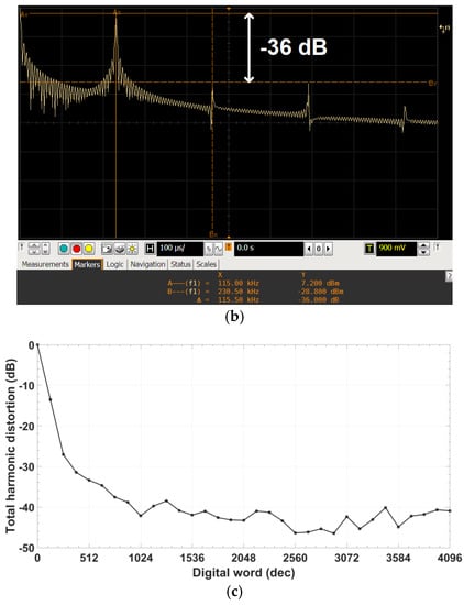
Figure 12.
Output quadrature signals measurements: (a) Screenshot of the oscilloscope for the digital code #500; (b) Spectral analysis of the output signal for the digital code #500; and (c) Total harmonic distortion of the output quadrature signals.
Table 2.
Oscillator measured performances.
The drift in the value of the programmed frequency due to the effects of the temperature in the oscillator has been characterized using a thermal chamber Fitoterm 22E from Aralab (Aralab Headquarters, Sintra, Portugal) in the range from −40 to 120 °C (Figure 13a). The proposed oscillator shows a slope error in the frequency programmability, lower than 12.9% from room temperature up to 120 °C and less than 8.7% for variations from room temperature down to −40 °C. Figure 13b shows the frequency programmability after the slope error has been corrected. Then, the maximum relative error is reduced down to 1.5% and absolute mean error to below 0.71% (Figure 13c).
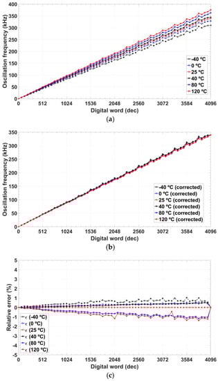
Figure 13.
Oscillation frequency for a temperature range from −40 to 120 °C: (a) measured; (b) slope error corrected; and (c) relative error after correction.
Comparing these performances with other previous works in the literature [18,19,20], only [18] presents a monolithic CMOS digitally programmable quadrature oscillator, but its resolution is limited to 6-bit, and the oscillation frequency (0.3 to 1.3 MHz) is nonlinear and inversely proportional to the digital word. In [19], the programmability resolution is 12-bit and the control is linear for a frequency range from 48 to 92 kHz, but it only integrates the active cell while the programmable element is implemented using external components, being non-compatible with low-voltage low-power operation. In [20], the oscillation frequency (from 29 to 230 kHz) lies within our target frequency range, but with non-linear analog control: the oscillation frequency is set by changing a transconductance parameter from 14 to 2.8 mS, while relies on external integrating 1 nF capacitors not suitable for on-chip solutions. Thus, to the best of the authors’ knowledge, this is the first fully integrated high resolution quadrature sinusoidal oscillator on the proposed frequency range with linear digital control compatible with the two key requirements of portable systems: low-voltage low-power operation and reduced size.
4. Application to Impedance Characterization
The suitability of the proposed quadrature oscillator as signal source for an IS micro-instrument is herein analyzed. For this, the selected test impedance configuration emulates the real impedance configuration known as Randles cell [10]: the target impedance is connected to a standard setup circuit consisting on an OpAmp, configured as an auto-balancing bridge with a feedback resistor (Figure 14).
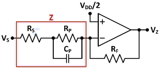
Figure 14.
Test impedance with an auto-balancing bridge.
For this circuit, when a sinusoidal signal excites the input of impedance , the output signal is given by:
In this way, it is possible to recover both magnitude and phase (related to the resistance and reactance components of the complex impedance), by next applying a synchronous quadrature demodulator using the signals provided by the proposed microelectronic stimulation circuit (Figure 1).
The first test impedance components selected are (Figure 14) , , and . Oscillator reliability was verified by comparing the obtained results to those achieved using a commercial 33522A AWG arbitrary waveform generator (Keysight Technologies, Santa Rosa, CA, USA) as signal source. Recovered impedance magnitude and phase are shown in Figure 15a,b. Besides, the feasibility of applying this technique for impedance characterization was verified using a GW-Instek 8101G LCR Meter (Good Will Instrument, Taipei, Taiwan). LCR measurement results in impedance magnitude and phase recovery are also included in Figure 15a,b. Magnitude errors are below 7% up to 330 kHz and phase errors are below 6% up to 340 kHz (Figure 15c). Absolute mean errors using the presented oscillator compared to the LCR-meter measurements are 2.21% for impedance magnitude and 1.17% for phase readout.
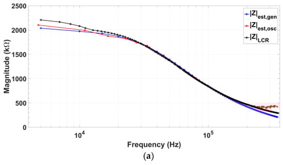
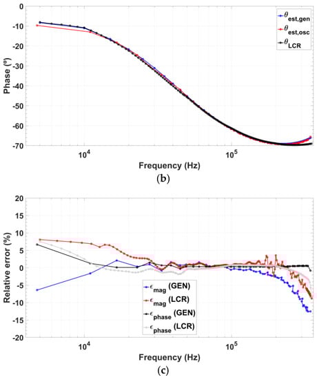
Figure 15.
Impedance measurement applying input quadrature signals generated by the fabricated oscillator prototype (red), commercial waveform generator (blue) and commercial 8101G LCR meter (black): (a) Impedance magnitude recovery; (b) Impedance phase recovery; and (c) Recovery errors for both magnitude and phase using the proposed integrated oscillator compared to the results applying the commercial AWG and the values measured by the LCR-meter.
Next, the designed oscillator has been tested as a stimulation module in a biological impedance measurement system for protein detection. Complex impedance component values were selected according to real measurements shown in the literature [10]: , , , and . For a suitable comparison, oscillator amplitude has been limited to 100 mV, considered as a typical input signal amplitude for this application. Figure 16 shows the impedance magnitude and phase obtained using the integrated oscillator compared to the value obtained using the commercial LCR-meter. Absolute recovery error of impedance magnitude always remains below 5%, while phase recovery error is below 5% for a frequency range from 34 to 337 kHz (90% of the oscillator total frequency range).
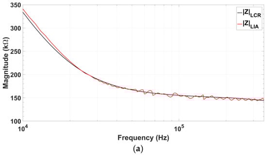
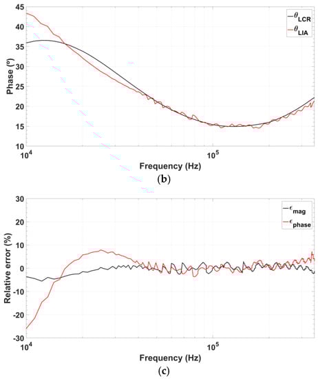
Figure 16.
Comparison of the impedance values measured using the signals from the proposed quadrature oscillator prototype (red) and those obtained using the commercial 8101G LCR-meter (black) for impedance values measured in protein detection: (a) Recovered impedance magnitude; (b) Recovered impedance phase, and (c) Relative error of both magnitude and phase.
These measurements have been done at fixed 100 mVpp excitation and nominal fixed 2 gain for the Randles cell at medium frequency range, but applied over the entire frequency range. However, it has to be noted that at the low frequency range impedance increases, reducing the system gain and thus the output signal, modifying the measurement conditions. On the contrary, at the high frequency range, impedance under test decreases, and therefore system gain must be reduced to keep the voltage measurement conditions almost constant. For an in-depth study of those effects, we have made new measurements with different gain conditions associated to the three frequency (low, medium, high) ranges: a gain of 4.5 in a 10 to 50 kHz span, a gain of 2 in a 50 to 250 kHz span, and a gain of 1.5 from 250 to 350 kHz. Figure 17 shows these measurements, displaying errors below 5%. In this way, it is possible to perform a fast impedance coarse characterization at constant gain for the Randles cell, or an accurate characterization using a configurable gain cell.
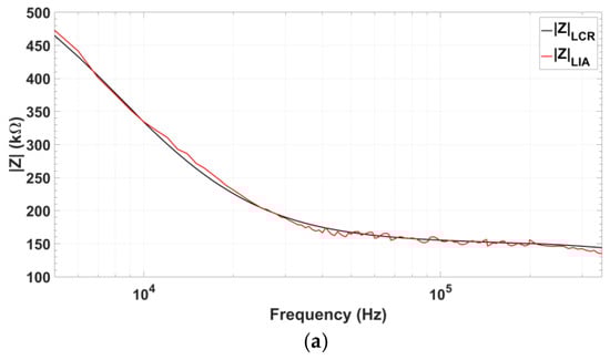
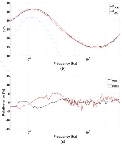
Figure 17.
Comparison of the impedance values measured using the signals from the proposed quadrature oscillator prototype (red) and those obtained using the commercial 8101G LCR-meter (black) for impedance values measured in protein detection, but employing a different gain setup for the three frequency ranges: low (5–50 kHz), medium (50–250 kHz), and high (250–350 kHz). (a) Recovered impedance magnitude; (b) Recovered impedance phase, and (c) Relative error of both magnitude and phase.
5. Conclusions
A novel CMOS 1.8 V–0.18 µm digitally programmable analog quadrature oscillator has been designed to be used as a stimulation system for phase sensitive detection signal recovery applications. It has been fabricated and tested, showing a linear frequency control ranging from 10 to 345 kHz, total power consumption lower than 0.77 mW, and active area of 0.129 mm2. Experimental tests show good performance as a self-contained signal generator in general purpose impedance PSD-based measurement applications, as proved by the comparison with the results achieved using a commercial LCR-meter. By properly limiting the maximum signal amplitude, its suitability as actuator system in biological impedance characterization has been also tested using an impedance protein model, successfully recovering both module and phase. Global characteristics make this design a highly suitable choice as a signal generation module for instrument-on-a-chip devices. To the best of the authors’ knowledge, this is the unique self-contained quadrature stimulation system, low-voltage low-power compatible and featuring such high frequency resolution over such a wide linear tuning range. In addition, to further increase the frequency into the MHz range, the gain-bandwidth product and bandwidth of the active elements (OpAmps and CS/CD network) should be increased at the cost of jeopardizing power consumption, besides redesigning the nominal values of resistors and capacitors.
Author Contributions
All authors equally contributed to the content of this article.
Funding
This research was funded by MINECO-FEDER, UE, grant number TEC2015-65750-R.
Acknowledgments
Authors would like to acknowledge the use of Servicio General de Apoyo a la Investigación (SAI), Universidad de Zaragoza.
Conflicts of Interest
The authors declare no conflict of interest. The founding sponsors had no role in the design of the study; in the collection, analyses, or interpretation of data; in the writing of the manuscript, and in the decision to publish the results.
References
- Liu, H.; Zhang, C.; Weng, Z.; Guo, Y.; Wang, Z. Resonance Frequency Readout Circuit for a 900 MHz SAW Device. Sensors 2017, 17, 2131. [Google Scholar] [CrossRef] [PubMed]
- D’Amico, A.; De Marcellis, A.; Di Carlo, C.; Di Natale, C.; Ferri, G.; Martinelli, E.; Paolesse, R.; Stornelli, V. Low-voltage low-power integrated analog lock-in amplifier for gas sensor applications. Sens. Actuators B Chem. 2010, 144, 400–406. [Google Scholar] [CrossRef]
- García-Romeo, D.; Pellejero, I.; Urbiztondo, M.A.; Sesé, J.; Pina, M.P.; Martínez, P.A.; Calvo, B.; Medrano, N. Portable low-power electronic interface for explosive detection using microcantilevers. Sens. Actuators B Chem. 2014, 200, 31–38. [Google Scholar] [CrossRef]
- Maya-Hernández, P.M.; Álvarez-Simón, L.C.; Sanz-Pascual, M.T.; Calvo-López, B. An Integrated Low-Power Lock-In Amplifier and its Application to Gas Detection. Sensors 2014, 14, 15880–15899. [Google Scholar] [CrossRef] [PubMed]
- He, D.; Morgan, S.P.; Trachanis, D.; van Hese, J.; Drogoudis, D.; Fummi, F.; Stefanni, F.; Guarnieri, V.; Hayes-Gill, B.R. A Single-Chip CMOS Pulse Oximeter with On-Chip Lock-In Detection. Sensors 2015, 15, 17076–17088. [Google Scholar] [CrossRef] [PubMed]
- Fu, J.; Wang, X.; Wei, T.; Wei, M.; Shen, Y. A Cost-Effective Geodetic Strainmeter Based on Dual Coaxial Cable Bragg Gratings. Sensors 2017, 17, 842. [Google Scholar] [CrossRef] [PubMed]
- Giaconia, C.G.; Greco, G.; Mistretta, L.; Rizzo, R. Exploring FPGA-Based Lock-In Techniques for Brain Monitoring Applications. Electronics 2017, 6, 18. [Google Scholar] [CrossRef]
- Ciccarella, P.; Carminati, M.; Ferrari, G.; Bianchi, D.; Grillanda, S.; Morichetti, F.; Melloni, A.; Sampietro, M. Impedance-Sensing CMOS Chip for Noninvasive Light Detection in Integrated Photonics. IEEE Trans. Circuits Syst. II Express Briefs 2016, 63, 929–933. [Google Scholar] [CrossRef]
- Zong, X.; Zhang, Z.; Zhu, R. Ultra-miniaturized Glucose Biosensor Using Zinc Oxide Nanorod-based Field Effect Transistor. In Proceedings of the IEEE Sensors Conference, Glasgow, UK, 29 October–1 November 2017; pp. 1389–1391. [Google Scholar]
- Manickam, A.; Chevalier, A.; McDermott, M.; Ellington, A.D.; Hassibi, A. A CMOS Electrochemical Impedance Spectroscopy (EIS) Biosensor Array. IEEE Trans. Biomed. Circuits Syst. 2010, 4, 379–390. [Google Scholar] [CrossRef] [PubMed]
- Blair, D.P.; Sydenham, P.H. Phase sensitive detection as a means to recover signals buried in noise. J. Phys. E Sci. Instrum. 1975, 8, 621–627. [Google Scholar] [CrossRef]
- Meade, M.L. Lock-In Amplifiers: Principles and Applications; Peter Peregrinus Ltd.: London, UK, 1983. [Google Scholar]
- Li, H.; Liu, X.; Li, L.; Mu, X.; Genov, R.; Mason, A.J. CMOS Electrochemical Instrumentation for Biosensor Microsystems: A Review. Sensors 2017, 17, 74. [Google Scholar] [CrossRef] [PubMed]
- García-Romeo, D.; Valero, M.R.; Medrano, N.; Calvo, B.; Celma, S. A High Performance LIA-Based Interface for Battery Powered Sensing Devices. Sensors 2015, 15, 25260–25276. [Google Scholar] [CrossRef] [PubMed]
- Márquez, A.; Pérez-Bailón, J.; Martínez, P.A.; Calvo, B.; Medrano, N. A CMOS low-power 12-bit digitally programmable analog sinusoidal actuation system. In Proceedings of the IEEE International Instrumentation and Measurement Technology Conference, Turin, Italy, 22–25 May 2017. [Google Scholar]
- Hammerschmied, C.M.; Huang, Q. Design and implementation of an untrimmed MOSFET-only 10-bit A/D converter with −79 dB THD. IEEE Int. J. Solid-State Circuits 1998, 33, 1148–1157. [Google Scholar] [CrossRef]
- Carlosena, A.; Martínez, P.A.; Porta, S. An improved Wien bridge oscillator. IEEE Trans. Circuits Syst. 1990, 37, 543–546. [Google Scholar] [CrossRef]
- Alzaher, H.A. CMOS digitally programmable quadrature oscillators. Int. J. Circuit Theory Appl. 2008, 36, 953–966. [Google Scholar] [CrossRef]
- Biolek, D.; Biolková, V.; Kolka, Z.; Bajer, J. Digitally-Controlled Quadrature Oscillators Employing Modified CDBAs. In Proceedings of the International Conference on Emerging Trends in Engineering and Technology (ICETET), Phuket, Thailand, 7–8 December 2013; pp. 40–46. [Google Scholar] [CrossRef]
- Sotner, R.; Jerabek, J.; Prokop, R.; Kledrowetz, V. Simple CMOS voltage differencing current conveyor-based electronically tunable quadrature oscillator. Electron. Lett. 2016, 52, 1016–1018. [Google Scholar] [CrossRef]
© 2018 by the authors. Licensee MDPI, Basel, Switzerland. This article is an open access article distributed under the terms and conditions of the Creative Commons Attribution (CC BY) license (http://creativecommons.org/licenses/by/4.0/).