Abstract
Due to the strong electronegativity of oxygen ions, the valence band maximum (VBM) that is derived from the O 2p orbital leads to strong localization, as well as further heavy hole mass and low hole mobility, which makes it extremely difficult to obtain high-conductivity p-type transparent conductive materials. Herein, we propose the strategy of multiple anions through the introduction of weaker electronegative nitrogen, in consideration of the delocalization on VBM, as well as the stability of octahedral anion cages. As such, first-principles calculations in the framework of density functional theory (DFT) are used for this work. Crystal structure prediction software USPEX (version 2023.0) was adopted to investigate the N-O appropriate ratio in CaTiO3−xNx (0 ≤ x ≤ 1) to balance the high transmission of light and highly favorable dispersion at the VBM. Furthermore, the p-type TCO performance of CaTiO3-xNx was evaluated based on the hole effective mass, hole mobility, and conductivity. The effectiveness of modulating p-type TCO through N-O multiple anions was also evaluated through defect formation energy and ionization energy. Ultimately, the construction of a CaTiO3-xNx/Si heterojunction and band alignment were considered for practical application. This approach attempts to boost the diversity of p-type perovskite-based TCOs and opens a new perspective for engineering and innovative material design for sustainable TCOs demand.
1. Introduction
In recent years, transparent conductive films have played a crucial role in various fields, such as solar cells, smart electronic products, liquid crystal displays, and conductive glass curtain walls, owing to their unique photoelectric properties. It is estimated that the global market size of transparent conductive films will reach 1.27 billion US dollars by 2029 [1]. Among them, n-type ITO (indium-doped tin oxide) has occupied 90% of the transparent conductive film market, owing to its excellent photoelectric properties, while the share of p-type transparent conductive oxides is relatively rare. This situation is mainly caused by the strong localization of the valence band top of p-type oxides, which leads to a low hole conductivity and, thus, severely limits the application and development of high-performance p-type transparent conductive oxides in transparent electronic devices [2]. Therefore, the exploitation of high-performance p-type transparent conductive oxides and their application in heterojunction devices are of great significance to research.
Transparent conductive oxides (TCOs) need to meet two key technical requirements: one is spectral transmittance [3]. To fully utilize sunlight, TCO-coated glass needs to have a transmittance of ≥80%. The other is electrical conductivity. TCO conductive films improve the film’s conductivity through doping, with minimum resistivity reaching the 10−5 Ω·cm level. Currently, n-type electron-conducting TCOs have been commercialized, but p-type TCOs are still in the early stages. The key challenge for p-type TCOs lies in how to reduce the strong localization of the valence band formed by O 2p states in metal oxides [4].
Over the past decades, continuous efforts have been made to try to solve this problem. In 1997, Kawazoe et al. first reported the p-type transparent conductive properties of CuAlO2 with a delafossite structure, and they proposed a novel approach—the Chemical Modification of the Valence Band (CMVB) theory [5]. This theory creatively proposes the use of cations with a full shell d10, as well as their energy levels equivalent to the O 2p levels, and then cation and anion form anti-bonding states through orbital hybridization, thereby weakening the localization effect of the holes near the valence band edges. This ultimately achieves the goal of improving p-type conductivity. Based on this, numerous delafossite-structured AMO2 materials are widely studied in p-type TCO films [6,7], e.g., Cu-based CuAlO2, CuCrO2, CuScO2, CuYO2, and CuGaO2, as well as Ag-based AgCrO2, AgGaO2, and AgCoO2. Limited by the existence of strongly electronegative oxygen ions, the room-temperature p-type conductivity of CuAlO2 only reaches up to 1 S cm−1 to date, which lags far behind that of the industrial standard n-type transparent conducting oxides [8]. Therefore, there is still an urgent demand to find an appropriate path to achieve high-performance p-type TCOs.
Perovskite oxides gradually came into the view of researchers, owing to their natural high light transmittance from a wide optical gap (>3.0 eV), adjustable band edge from doping, and excellent electrical properties from their extraordinary crystal structures [9]. Kim et al. reported that La-doped BaSnO3 obtained high mobility at room temperature while retaining its optical transparency [10]. In single crystals, the mobility reached 320 cm2V−1s−1 at a doping level of 8 × 1019 cm−3. In epitaxial films, the maximum mobility was 70 cm2V−1s−1 at a doping level of 4.4 × 1020 cm−3. From this perspective, it reveals the excellent electrical potential of perovskite oxides as TCOs. Sr-doped LaCrO3 with 50% Sr on the La site, arguably forming a mixed cation perovskite, resulted in p-type conductivity of 50 S cm−1, but at the cost of a 50% loss in transmission [11]. The p-type K-doped BaSnO3 showed a hole mobility of 0.30 cm2V−1s−1 at a carrier concentration of 1013 cm−3, giving low overall conductivity [12]. The rhombohedral double perovskite Ba2BiTaO6 with K on the Ba site was demonstrated to display a hole mobility of 30 cm2V−1s−1, but with an extremely low carrier concentration (1014 cm−3) and, therefore, low conductivity [13]. The application of perovskite as a p-type TCO is still in its initial stage, and the optimization of the modulation technology is still ongoing.
Recently, the modulation strategy of multiple anions played an important role in the physical and chemical properties of materials. Kageyama et al. [14] mixed other anions in traditional single-anion compounds and changed the number, position, and size of the substituted anions to transform energy level splitting under the crystal field; this was done to further the control of the energy band, and ultimately develop new applications of traditional materials, such as photocatalytic applications (Zr2ON2) (N1-xOx) [15], battery applications (LiFeSO4F) [16], polychromatic applications (Ca3ReO5Cl2) [17], superconductivity applications (Sr2CuO2Cl2) [18], and so on. At present, research that is based on perovskite-type TCOs mostly focuses on the modulation of metal cations [10,12]; however, there is little research on strategies of multiple anions to design p-type TCOs. In consideration of the prominent effect of multiple anions on the electrical properties of materials, this work will carry out the introduction of weaker electronegative nitrogen to exploit perovskite as a candidate for p-type TCOs.
This work was conducted based on parent CaTiO3 with a natural wide gap (>3.0 eV) and lead-free resource. The paper is organized as follows. First, the O-N ratio in CaTiO3-xNx (0 ≤ x ≤ 1) is searched and discussed, focusing on their crystal structures, band structures, and optical properties. Second, the performance of CaTiO3-xNx is evaluated as a p-type TCO application, focusing on elastic constants, deformation potential, effective mass, mobility, and conductivity. The effectiveness of modulating p-type TCOs with a NO defect in CaTiO3 is evaluated through defect formation and ionization energy. In conclusion, the photovoltaic heterojunction is constructed, and the band alignment is carried out based on p-type CaTiO3-xNx on a Si substrate.
2. Results and Discussion
2.1. Search for O-N Ratio in CaTiO3-xNx (0 ≤ x ≤ 1)
Using the crystal structure prediction software, USPEX, the O-N ratio in CaTiO3-xNx (0 ≤ x ≤ 1) was predicted through variational control. 1N, 2N, 3N, and 4N were sequentially doped into the parent phase CaTiO3 (CTO) in a 2 × 2 × 2 supercell (40 atoms), with the corresponding x values of 0.025, 0.05, 0.075, and 0.1, respectively. After global searching, stable crystal structures were obtained at different doping concentrations and are shown in Figure 1. In Figure 1a, after replacing O with 1/24 N in the 40-atom supercell, the crystal structure transforms from the orthorhombic phase of the parent phase CaTiO3 to a more symmetrical tetragonal phase (space group: P4/mmm). As the number of N continues to increase, the symmetry of the crystal structure decreases to its minimum (space group: P1), making it difficult to stably exist in terms of energy. Therefore, in CaTiO3-xNx (0 ≤ x ≤ 1), the thermodynamic stability of the crystal is optimal when the N concentration is 0.025, which is the best doping concentration in the parent phase CaTiO3.
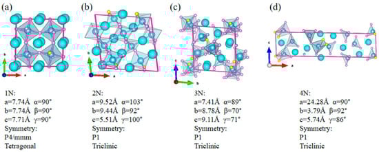
Figure 1.
The crystal structure of a CaTiO3-xNx (0 ≤ x ≤ 1) supercell, searched by USPEX software: (a) 1N (x value: 0.025), (b) 2N (0.05), (c) 3N (0.075), and (d) 4N (0.1).
Subsequently, the electronic structure of the CaTiO2.975N0.025 supercell (CTON) was calculated using HSE06 hybrid functional, and the results are shown in Figure 2b. Compared to the CaTiO3 band structure, where the valence band top is mainly contributed by O 2p orbitals (Figure 2a), in the CTON system, two impurity energy levels are introduced at the valence band top due to the substitution of weak electronegative N doping, resulting in a decrease in the optical gap width from 3.4 eV to 2.73 eV. Since N doping only acts on the valence band, the position of the conduction band bottom in the CTON system remains unchanged at around 3.0 eV. Considering the high transparency of transparent conductive oxides, candidate materials need to have a band width that is greater than 3.0 eV. Therefore, further substitution is needed in the CTON system to increase the bandwidth. As the conduction band in the CaTiO3 band structure is mainly contributed by Ti 3d orbitals, one Zr atom with a higher orbital level is selected for the substitution on one Ti site, aiming to promote the upward lifting of the conduction band and ultimately increase the band width of CTON to the ideal range.
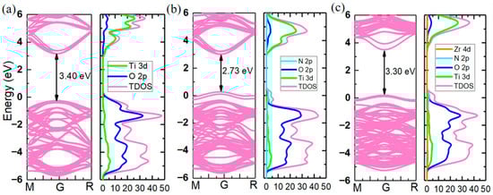
Figure 2.
Band structure and density of states through HSE06 hybrid functional calculation: (a) CaTiO3, (b) CaTiO2.975N0.025, and (c) CaTi2.975Zr0.025O2.975N0.025.
The crystal structure of the CaTi2.975Zr0.025O2.975N0.025-doped system (CTZON) is shown in Figure 3a. The Zr cation has a bigger ionic radius (0.72 Å) than the Ti cation (0.605 Å), under the VI coordination number. Therefore, the introduction of one Zr cation brings out a degree of octahedron distortion after fully relaxing. Owing to the tolerance of the octahedral oxygen cage, after Zr substitution, the crystal structure of the system remains tetragonal, and the symmetry slightly decreases to P4MM. The electronic structure is shown in Figure 2c, and occurred after the HSE06 hybrid functional calculation was completed. Due to the substitution of one Zr atom for one Ti site, the conduction band position is shifted to a higher energy level, resulting in an expansion of the band width from 2.73 eV to 3.30 eV, making the N-doped system meet the high transparency requirements.
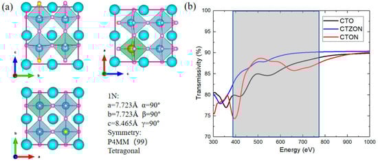
Figure 3.
(a) Crystal structure of CaTi2.975Zr0.025O2.975N0.025-doped system (CTZON), (b) comparison of transmittance of three types of thin-film materials.
The optical properties of materials can be obtained from the frequency-dependent complex dielectric constant through VASPKIT (version 1.5.0) [19], and the calculation Formula (1) is as follows:
Among them, and are, respectively, the real and imaginary parts of the dielectric constant, and is the photon frequency.
The transmittance of a material is related to its reflectivity , absorption coefficient , and thickness d in the incident direction. Formula (2) is as follows:
The calculation Formulas (3) and (4) for reflectivity and the absorption coefficient are as follows:
In the formulas for reflectivity and the absorption coefficient, and are for the refractive index and extinction coefficient, respectively. The calculation Formulas (5) and (6) are for the relationship between the real and imaginary parts of the dielectric constant and are as follows:
After a series of calculations of optical parameters, the transmittance of the doped film is shown in Figure 3b. The transmittance of CTZON is significantly better than that of the CTO and CTON systems in the visible light range of 390–780 nm, and the transmittance of the CTZON system reaches up to 90% in the visible light range.
2.2. Performance Evaluation of CaTiO3-xNx (0 ≤ x ≤ 1) as p-Type TCO Applications
Adopting an approximate method based on deformation potential theory to study the p-type transport characteristics of CTZON, the mobility formula is as follows [20]:
Among them, ћ is the reduced Planck constant, e is the electron charge, is the elastic constant, V0 is the lattice volume, m* is the effective mass of the carrier (electrons for the bottom of the conduction band and holes for the top of the valence band), kB is the Boltzmann constant, T is the temperature of 300 K, and is the deformation potential, defined by the change in band edge energy divided by the change in volume. The effective mass m* of the valence band holes in the researched system is obtained using EMC software (version 1.0) based on the finite difference method.
The elastic constants, deformation potential, effective mass, and mobility obtained through calculations are shown in Table 1. Due to the strong oxygen localization in CTO, the dispersed morphology of the valence band top produces a hole effective mass of 9.72 m0, which is not conducive to the efficient migration of hole carriers. This conclusion is close to the hole effective mass of 9.8 m0 that was reported by Wunderlich et al. for SrTiO3 at the G point [21]. After N doping, the effective mass of the holes in CTON is significantly improved compared to CTO, with an effective mass reduction to 2.09 m0. This is mainly due to the formation of two new, sharper impurity energy levels from the weaker localization at the top of the valence band after N doping. However, Zhong et al. found that the effective mass of holes needs to be reduced to below 1.5 m0 in order to facilitate efficient transport of hole carriers [22]. In the CTZON system, one Zr atom with strong metallicity further optimizes the atomic bonding in the doping system, thereby improving the local morphology of the valence band top. After calculation, a hole effective mass of 1.24 m0 is obtained, indicating that the doping ratio in CTZON has achieved the goal of efficient modulation of CaTiO3 for p-type transparent conductive oxide applications.

Table 1.
Elastic constants (C), valence band deformation potential (Ev), effective hole mass (m*), hole mobility (μ), and conductivity (σ) of three materials.
After calculating the mobility, it was found that compared to the mobility of 1.49 cm2/v/s in the CTO system, the CTON system achieves a mobility of 39.73 cm2/v/s, which is 10 times higher; the mobility of the CTZON system is 158.73 cm2/v/s, which is 102 times higher and significantly improves the transport ability of the valence band top holes. In a supercell with 40 atoms, the doping concentration of one N atom was calculated to be 5.51 × 10¹⁹/cm3. The conductivity of the system was calculated using the formula σ = neμ (n-doping concentration, e-elementary charge, and μ-mobility) and the results as shown in Table 1. Compared to the weak conductivity of 13 S/cm in the CTO system, the CTON system achieves a conductivity of 349 S/cm, while the conductivity of the CTZON system is greatly improved, reaching 1397 S/cm, which is far superior to the conductivity level of traditional p-type delafossite-based transparent conductive oxides [8].
The effectiveness of modulating p-type TCO with a NO defect and the compensation effect of a VO defect on p-type doping can be evaluated by the formation energy of defects [23]. The calculation formula for defect formation energy is as follows:
In the equation, Etot represents the total energy of one supercell containing a defect D with q charge, Epure is the total energy of a perfect system of the same size, ni is for the change in the number of atoms in the system before and after introducing the defect (adding atoms to the system (ni < 0) and removing atoms from the system (ni > 0)), μi is for the atomic chemical potential of the constituent elements, and the Fermi level Ef refers to the energy position EV (Perfect) of VBM in the perfect system.
We introduced a correction term to correct the electrostatic potential difference between the defective supercell and perfect supercell: ΔV = Vave (D, q) − Vave (perfect, 0), where Vave (D, q) and Vave (perfect, 0) are the average electrostatic potentials of the defective supercell and perfect supercell, respectively.
The calculation found that the formation energy of the NO defect is −2.62 eV, indicating that N-substituted O is prone to occur and the defect can exist stably. The formation energy of the VO defect is 2.07 eV, testifying that due to the stabilizing effect of TiO6 octahedral oxygen cages in the CTO parent phase, the VO defect is not easily generated. Therefore, the compensation effect of the VO defect on the N-substituted modulation of CaTiO3 for p-type TCO is not prominent. The stability and effectiveness of N-substituted modulation are ensured through the calculation of formation energy.
Further research was conducted on the ionization energy of the defects in the CTZON system to ensure that the acceptor level position of the NO defects was shallow for ionization. Using a hydrogen-like model, the ionization energy of the material was calculated based on the effective mass of carriers and the relative dielectric constant [24]. The ionization energy is defined as the energy difference between the acceptor/donor energy levels and the VBM state. The formula for calculating the ionization energy of one single hole state is as follows:
In this equation, 13.6 eV is the ground state ionization energy of hydrogen atoms, m* is the effective mass of the system, m0 is the effective mass of the elementary charge, and ε is the relative dielectric constant. After calculating the relative permittivity through VASP software (version 5.4.4), it is known that the ε of the CTO system is 10.81 and the ε of the CTZON system is 11.20. Based on the calculated effective mass of the holes in Table 1, here, the ionization energies at the valence band tops of CTO and CTZON are 1.13 eV and 0.13 eV, respectively. N-doping effectively reduces the ionization energy of the valence band top and facilitates the formation of p-type hole carriers.
2.3. Photovoltaic Heterostructure Construction and Band Alignment Based on p-Type CaTiO3-xNx
The interface modeling adopts the superlattice method with periodically repeating layers, and the superlattice based on p-type CTZON and Si is constructed through Material Studio software (version 2017) for the application of p-i photovoltaic heterostructure. The (001) crystal plane of CTZON (a = b = 7.723 Å, c = 20.251 Å, α = β = γ = 90°), and the (011) crystal plane of Si (a = b = 7.734 Å, c = 19.570 Å, α = β = γ = 90°) were selected for interfacial matching, and the lattice mismatch was calculated to be 0.14%, indicating that the two have good lattice matching abilities and can effectively avoid internal stress at the interface. The CTZON/Si heterostructure is shown in Figure 4a,b. In Figure 4a, Si atoms tend to bond with O atoms in the TiO2 layer, effectively reducing the occurrence of oxygen vacancies at the interface and eliminating the negative impact on the p-type TCO properties of N-doped CaTiO3. From Figure 4b, it can be seen that the Si (011) interface matches well with the CTZON (001) interface.
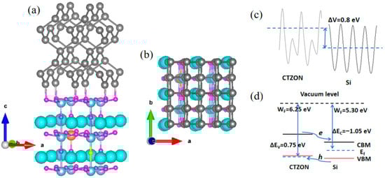
Figure 4.
(a,b) show the CTZON/Si heterostructure, (c) the average electrostatic potential difference between CTZON and Si, and (d) the band edge offset and band alignment type of CTZON/Si.
To investigate the types of band alignment of the CTZON/Si heterostructure, the average electrostatic potential alignment method was used for research [25,26]. First, the average electrostatic potential of two materials based on the vacuum energy levels was obtained, as shown in Figure 4c. Considering the Fermi levels of the two materials, the work functions of the two materials were obtained, as shown in Figure 4d. It can be seen that the difference in work functions between the two materials is 0.95 eV. According to the positions of the valence band top and conduction band bottom of CTZON and Si, the valence band deviation of the two materials was calculated using ΔEVBM = −0.2 eV, and the conduction band deviation ΔECBM = −2.0 eV. Furthermore, it can be inferred that the band offset of CTZON and Si is ΔEV = 0.75 eV, and the band offset is ΔEC = −1.05 eV. From the band offsets, it can be concluded that the CTZON/Si heterostructure belongs to the type II stagger, which can effectively promote electron–hole spatial separation and the efficient transport of hole carriers.
3. Methods
Theoretical simulation calculations were carried out using the Vienna Ab Initio Simulation Package (VASP) [27,28], while the projector augmented wave (PAW) method was used to describe the ionic potentials, including the effect of the core electrons [29,30]. For calculation accuracy, the Brillouin Zone (BZ) summation was calculated with Monkhorst–Pack k-point intervals that were limited below 0.04 Å−1 for the supercells [20]. A plane-wave cutoff energy of 520 eV was employed in all calculations. All obtained structures were geometrically fully relaxed until the force convergence on each ion was reduced below 0.01 eV Å−1 [31]. We adopted a convergence criterion of 10−6 eV, which is adequate for electronic self-consistent iteration. For the calculations of band structures, we used the HSE06 functional to achieve more accurate values of band gaps [32]. In this work, the Perdew–Burke–Ernzerhof (PBE) exchange–correlation (XC) functionals [33,34] were adopted to calculate the electronic properties.
Based on the genetic evolution algorithm with the principle of energy minimization, the universal structure predictor (USPEX) [35,36] was adopted to predict stable or metastable structures for any given composition. The prediction process was as follows: in the first generation crystal structure prediction, 200 initial structures were randomly generated after spatial symmetry operation; after comparing the enthalpy of relaxation structure formation, the most stable and metastable structures were selected and entered the next generation cycle; in each subsequent generation, an additional 60 crystal structures were obtained, with variable values of 50% inherited, 20% random, 20% soft mode mutation, and 10% lattice mutation. Continuous cycling was essential until the most stable component structure remained constant for the subsequent 20 generations to ensure global equilibrium. Then, the search cycle ended.
4. Conclusions
In this study, we used the strategy of multiple anions to modulate multifunctional perovskite oxides for the application of p-type TCOs against strong localization from the O 2p orbital at the VBM. From the enthalpy of formation, USPEX software finds that the N concentration with x = 0.025 in CaTiO3-xNx could maintain the stability of octahedral anion cages without the severe destruction of symmetry. Employing the HSE06 hybrid functional, it was predicted that the optical gap in the CTON supercell would slightly decrease to 2.73 eV. Furthermore, substituting one Zr atom with a higher orbital level at the Ti site was selected to elevate the conduction band minimum and, consequently, expand the gap width to 3.30 eV. Subsequently, the transmittance of CTZON was confirmed to reach up to 90% in the visible light range of 390–780 nm. After calculating electrical performance, the CTZON compound contributes 1.24 m0 of hole effective mass, 158.73 cm2/v/s of hole mobility, and 1397 S/cm of hole conductivity. Meanwhile, the formation energy of the NO defect with −2.62 eV estimates the effectiveness of modulating a p-type TCO through N-O multiple anions. Furthermore, the ionization energy of the NO defect, with 0.13 eV, confirmed the shallow acceptor energy for facilitating the formation of p-type hole carriers. Additionally, the (001)CTZON/(011)Si heterojunction was constructed with a 0.14% lattice mismatch, and the band alignment demonstrated that it belongs to a type II staggered heterojunction, which can effectively promote electron–hole spatial separation and the efficient transport of hole carriers. This work provides fundamental insights into the design of high-performance p-type transparent materials, and it is supposed to enrich the diversity of alternative perovskite-based TCOs.
Author Contributions
Conceptualization, Y.L.; Methodology, Y.L. and K.L.; Software, K.L. and H.C.; Validation, K.L., H.C., Y.W., S.Z. and L.B.; Formal analysis, Y.W. and S.Z.; Investigation, Y.L.; Resources, K.L. and S.Z.; Data curation, K.L., H.C., Y.W., S.Z. and L.B.; Writing – original draft, Y.L.; Writing – review & editing, Y.L., H.C., Y.W., S.Z. and L.B.; Visualization, Y.L.; Supervision, Y.L. and K.L.; Project administration, Y.L. and L.B.; Funding acquisition, Y.L. and H.C. All authors have read and agreed to the published version of the manuscript.
Funding
This work was financially supported by Henan Province Science and Technology Research Projects (Grant No. 232102231001 and 242102321090), a Zhumadian Research & Development Project (Grant No. ZMDSZDZX2023013), and Huanghuai University Research-Oriented Special Projects (Grant No. 2024XJGZLX20).
Institutional Review Board Statement
Not applicable.
Informed Consent Statement
Not applicable.
Data Availability Statement
The original contributions presented in this study are included in the article. Further inquiries can be directed to the corresponding authors.
Acknowledgments
The authors would like to thank all the reviewers participated in this review process.
Conflicts of Interest
There are no conflicts to declare.
References
- Sharma, B.; Rana, P.S. The bright and dark shades of transparent conducting perovskites: From science to global market. J. Phys. Conf. Ser. 2022, 2267, 012030. [Google Scholar] [CrossRef]
- Singh, J.; Bhardwaj, P.; Kumar, R. Progress in developing highly efficient p-type TCOs for transparent electronics: Comprehensive review. J. Electron. Mater. 2024, 53, 7179–7210. [Google Scholar] [CrossRef]
- Hautier, G.; Miglio, A.; Ceder, G. Identification and design principles of low hole effective mass p-type transparent conducting oxides. Nat. Commun. 2013, 4, 2292. [Google Scholar] [CrossRef]
- Zhang, K.H.L.; Xi, K.; Blamire, M.G.; Egdell, R.G. P-type transparent conducting oxides. J. Phys. Condens. Matter 2016, 28, 383002. [Google Scholar] [CrossRef] [PubMed]
- Kawazoe, H.; Yasukawa, M. P-type electrical conduction in transparent thin films of CuAlO2. Nature 1997, 389, 939–942. [Google Scholar] [CrossRef]
- Sheng, S.; Fang, G.; Li, C. P-type transparent conducting oxides. Phys. Status Solidi 2010, 203, 1891–1900. [Google Scholar] [CrossRef]
- Hu, L.; Wei, R.; Tang, X.; Lu, W.; Sun, Y. Design strategy for p-type transparent conducting oxides. J. Appl. Phys. 2020, 128, 140902. [Google Scholar] [CrossRef]
- Liu, K.; Wei, J.; Meng, L. Activating p-type conduction and visible transparency in delafossite CuAlO2 films: The critical role of the copper valence state transition. Mater. Today Phys. 2024, 40, 101304. [Google Scholar] [CrossRef]
- He, H.; Yang, Z.; Xu, Y. Perovskite oxides as transparent semiconductors: A review. Nano Converg. 2020, 7, 32. [Google Scholar] [CrossRef]
- Kim, H.J.; Kim, U.; Kim, H.M. High Mobility in a Stable Transparent Perovskite Oxide. Appl. Phys. Express 2012, 5, 061102. [Google Scholar] [CrossRef]
- Zhang, K.H.L.; Du, Y.; Papadogianni, A.; Bierwagen, O.; Sallis, S.; Piper, L.F.J.; Bowden, M.E.; Shutthanandan, V.; Sushko, P.V.; Chambers, S.A. Perovskite Sr-Doped LaCrO3 as a New p-Type Transparent Conducting Oxide. Adv. Mater. 2015, 27, 5191–5195. [Google Scholar] [CrossRef]
- Kim, H.M.; Kim, U.; Park, C.; Kwon, H.; Char, K. Thermally stable pn-junctions based on a single transparent perovskite semiconductor BaSnO3. APL Mater. 2016, 4, 056105. [Google Scholar] [CrossRef]
- Dahliah, D.; Rignanese, G.-M.; Hautier, G.J. Defect compensation in the p-type transparent oxide Ba2BiTaO6. Mater. Chem. C 2020, 8, 9352–9357. [Google Scholar] [CrossRef]
- Kageyama, H.; Hayashi, K.; Maeda, K.; Attfield, J.P.; Hiroi, Z.; Rondinelli, J.M.; Poeppelmeier, K.R. Expanding frontiers in materials chemistry and physics with multiple anions. Nat. Commun. 2018, 9, 772. [Google Scholar] [CrossRef]
- Streibel, V.; Scho, J.; Wagner, J.; Sirotti, E.; Munnik, F.; Sharp, I. Zirconium oxynitride thin films for photoelectrochemical water splitting. ACS Appl. Energy Mater. 2024, 7, 4004–4015. [Google Scholar] [CrossRef]
- Takamoto, S.; Shinagawa, C.; Motoki, D.; Nakago, K.; Li, W.; Kurata, I.; Ibuka, T. Towards universal neural network potential for material discovery applicable to arbitrary combination of 45 elements. Nat. Commun. 2022, 13, 2991. [Google Scholar] [CrossRef]
- Choi, K.Y.; Lee, S.; Lee, J.H.; Seong, M.J.; Choi, K.Y. Bosonic spinons in anisotropic triangular antiferromagnets. Nat. Commun. 2021, 12, 6453. [Google Scholar] [CrossRef]
- de la Torre, A.; Matteo, S.D.; Hsieh, D.; Norman, M.R. Implications of second harmonic generation for hidden order in Sr2CuO2Cl2. Phys. Rev. B 2021, 104, 035138. [Google Scholar] [CrossRef]
- Wang, V.; Xu, N.; Liu, J.C.; Tang, G.; Geng, W.T. VASPKIT: A User-Friendly Interface Facilitating High-Throughput Computing and Analysis Using VASP Code. Comput. Phys. Commun. 2021, 267, 108033. [Google Scholar] [CrossRef]
- Liang, Y.T.; Shao, G.S. First principles study for band engineering of KNbO3 with 3d transition metal substitution. RSC adv. 2019, 9, 7551–7559. [Google Scholar] [CrossRef] [PubMed]
- Wunderlich, W.; Ohta, H.; Koumoto, K. Enhanced effective mass in doped SrTiO3 and related perovskites. Phys. B Condens. Matter 2009, 404, 2202–2212. [Google Scholar] [CrossRef]
- Zhong, M.; Zeng, W.; Liu, F.S.; Tang, B.; Liu, Q.J. A member of p-type TCO family: Sn2TaxNb2-xO7 with a tunable band gap and controllable hole mobility. Mat. Sci. Eng. B 2021, 271, 115255. [Google Scholar] [CrossRef]
- Williamson, B.A.D.; Buckeridge, J.; Brown, J. Engineering valence band dispersion for high mobility p-type semiconductors. Chem. Mater. 2017, 29, 2402–2413. [Google Scholar] [CrossRef]
- Tablero, C. Acceptor and donor ionization energy levels in O-doped ZnTe. Comp. Mater. Sci. 2010, 49, 368–371. [Google Scholar] [CrossRef]
- Hinuma, Y.; Grüneis, A.; Kresse, G.; Oba, F. Band alignment of semiconductors from density-functional theory and many-body perturbation theory. Phys. Rev. B 2014, 90, 155405. [Google Scholar] [CrossRef]
- Scanlon, D.O.; Dunnill, C.W.; Buckeridge, J.; Shevlin, S.A.; Logsdail, A.J.; Woodley, S.M. Band alignment of rutile and anatase TiO2. Nat. Mater. 2012, 12, 798–801. [Google Scholar] [CrossRef] [PubMed]
- Kresse, G.; Hafner, J. Ab initio molecular dynamics for liquid metals. Phys. Rev. B 1993, 47, 558–561. [Google Scholar] [CrossRef] [PubMed]
- Kresse, G.; Hafner, J. Ab-initio molecular-dynamics simulation of the liquid-metal amorphous-semiconductor transition in germanium. Phys. Rev. B 1994, 49, 14251–14269. [Google Scholar] [CrossRef] [PubMed]
- Blöchl, P.E. Projector augmented-wave method. Phys. Rev. B 1994, 50, 17953–17979. [Google Scholar] [CrossRef]
- Kresse, G.; Joubert, D. From ultrasoft pseudopotentials to the projector augmented-wave method. Phys. Rev. B 1999, 59, 1758–1775. [Google Scholar] [CrossRef]
- Liang, Y.T. Exploring inorganic and nontoxic double perovskites Cs2AgInBr6(1−x)Cl6x from material selection to device design in material genome approach. J. Alloys Compd. 2021, 862, 158575. [Google Scholar] [CrossRef]
- Heyd, J.; Scuseria, G.E.; Ernzerhof, M. Hybrid functionals based on a screened Coulomb potential. J. Chem. Phys. 2003, 118, 8207, Correction in J. Chem. Phys. 2006, 124, 21. [Google Scholar] [CrossRef]
- Kresse, G.; Hafner, J. Ab initio molecular dynamics for open-shell transition metals. Phys. Rev. B 1993, 48, 13115. [Google Scholar] [CrossRef] [PubMed]
- Perdew, J.P.; Burke, K.; Ernzerhof, M. Generalized gradient approximation made simple. Phys. Rev. Lett. 1996, 77, 3865. [Google Scholar] [CrossRef] [PubMed]
- Oganov, A.R.; Glass, C.W. Crystal structure prediction using ab initio evolutionary techniques: Principles and applications. J. Chem. Phys. 2006, 124, 244704. [Google Scholar] [CrossRef]
- Glass, C.W.; Oganov, A.R.; Hansen, N. USPEX—Evolutionary crystal structure prediction. Comput. Phys. Commun. 2006, 175, 713–720. [Google Scholar] [CrossRef]
Disclaimer/Publisher’s Note: The statements, opinions and data contained in all publications are solely those of the individual author(s) and contributor(s) and not of MDPI and/or the editor(s). MDPI and/or the editor(s) disclaim responsibility for any injury to people or property resulting from any ideas, methods, instructions or products referred to in the content. |
© 2026 by the authors. Licensee MDPI, Basel, Switzerland. This article is an open access article distributed under the terms and conditions of the Creative Commons Attribution (CC BY) license.