Abstract
Synthesizable field-programmable gate arrays (FPGAs) have recently gained significant traction due to their low development costs and their ability to adapt to new process technologies. The successful adoption of synthesizable FPGAs requires robust methodologies for estimating the area characteristics of the FPGA tiles in the synthesizable FPGA fabrics. FPGA tile area is used to determine the physical lengths of an FPGA’s routing segments and is therefore crucial to ensuring the accurate benchmarking of newly proposed FPGA architectures. In this work, we present a methodology to estimate the area of synthesizable FPGA tiles across various semiconductor process technologies. The methodology leverages scaling trends in the area of synthesizable FPGA tiles and selected hierarchical blocks to derive scaling factors that can be used to scale the area of synthesizable FPGA tiles across process nodes. The results demonstrate that this methodology achieves a maximum absolute percentage error of less than 10% when scaling the area of synthesizable FPGA tiles across open-sourced 130 nm, 45 nm, 15 nm and 7 nm process nodes.
1. Introduction
Synthesizable FPGA fabrics offer a flexible and scalable approach to FPGA fabric design. These fabrics are described using hardware description languages and synthesized into netlists composed of standard cells using application-specific integrated circuit (ASIC) synthesis tools. The resulting netlists are then placed and routed using electronic design automation tools to generate complete physical layouts of the FPGA fabrics. Figure 1 shows a layout view of a synthesizable FPGA tile implemented using OpenLane/OpenROAD, a widely used open-source ASIC design toolchain [1,2,3], and the Skywater 130 nm standard cell library [4]. The configuration parameters for this tile are defined as follows: , , , , and . Here, k denotes the number of inputs per look-up table (LUT), N is the number of basic logic elements (BLEs) per cluster, W represents the channel width, indicates the input connectivity ratio between logic blocks and routing channels, and L is the segment length of the routing tracks.
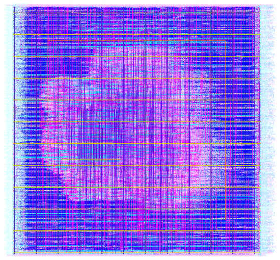
Figure 1.
Layout view of a synthesizable FPGA tile implemented using OpenLane/OpenROAD.
A key advantage of synthesizable FPGA fabrics is their scalability across semiconductor process nodes. This scalability is made possible by simply updating the standard cell libraries used during synthesis, placement, and routing. As a result, FPGA fabric designers can significantly reduce the time and effort required to migrate FPGA architectures to new technology nodes, making synthesizable fabrics an attractive option for future design considerations.
However, successful migration of synthesizable FPGA architectures to new process nodes still requires careful evaluation. Designers must ensure that the architecture remains efficient and reliable under the constraints of the new semiconductor technology. To facilitate this, FPGA architecture exploration tools are used to assess the area, performance, and other key metrics of synthesizable FPGA architectures across process nodes. These tools rely on accurate estimations of the area characteristics of the new FPGA tiles [5,6,7,8].
Reliable FPGA tile area estimation models allow designers to make informed architectural decisions without incurring the computational cost of a full backend implementation. As design complexity and process variability increase, the need for efficient and scalable area prediction becomes even more critical.
Determining FPGA tile area through physical design remains computationally expensive and time-consuming, particularly when evaluating a large design space with many architectural parameters. To address this issue, prior research has proposed using constant scaling factors to estimate the area of digital circuits across different technology nodes, showing promising accuracy in their application domains [9,10].
This study investigates the application of constant scaling factors specifically for synthesizable FPGA tile area estimation. We find that while existing scaling factors, such as those reported in [9,10], can be applied, they can introduce significant errors when applied to the area of synthesizable FPGA tiles. In some cases, these factors yield area estimation errors of up to 182%. This occurs because they are based on simplistic inverter-only circuits, which do not capture the complexity of standard cell-based FPGA layouts. To overcome this limitation, we refine the scaling methodology by incorporating the layout characteristics of standard cells and architectural features that are unique to FPGA fabrics. Our approach reduces area estimation errors from 182% to less than 10%, indicating a significant improvement in accuracy.
The goal of this research is to develop an efficient and accurate area estimation model for synthesizable FPGA tiles that can be applied across semiconductor process nodes without full physical implementation. Our main idea is to refine traditional scaling factor methods by incorporating information derived from the standard cell layouts used in FPGA tile synthesis. The key contributions of this paper are as follows:
- Analyze the limitations of existing scaling factor approaches when applied to synthesizable FPGA tiles.
- Introduce a refined scaling methodology that integrates standard-cell layout characteristics into the estimation process.
- Evaluate the accuracy of the proposed model on multiple open-source technology nodes and demonstrate a significant reduction in estimation error compared to previous methods.
2. Background
In previous work, we demonstrated the potential of machine learning for rapid FPGA tile area estimation [11,12]. Specifically, an Extreme Gradient Boosting (XGBoost) regression model was trained and tuned to predict the area of 7 nm fin field-effect transistor (FinFET) standard cell-based FPGA tiles using a set of user-defined architectural parameters. These parameters serve as inputs to the model, which estimates the tile area within seconds and achieves a maximum absolute percentage error of less than 10%.
However, the machine learning model from previous work is limited to a single technology node and its associated standard cell library. As a result, the model cannot generalize across different semiconductor process nodes without retraining. Enabling multi-node predictions would require a significantly larger and more diverse dataset covering multiple technology nodes.
To overcome this limitation, we investigate a methodology that enables area estimation across process nodes without retraining or requiring large datasets. Rather than relying solely on machine learning, we use process scaling factors to estimate FPGA tile area at a new node based on a known area at a base node. This approach leverages the consistent scaling behavior of synthesizable FPGA designs and can substantially reduce computational requirements. Previous work has shown that this approach can be used reliably to scale the implementation area of inverter-only circuits across multiple process nodes [9]. However, its application to FPGA tile implementation area has not been investigated. The flow of the proposed methodology is shown in Figure 2.
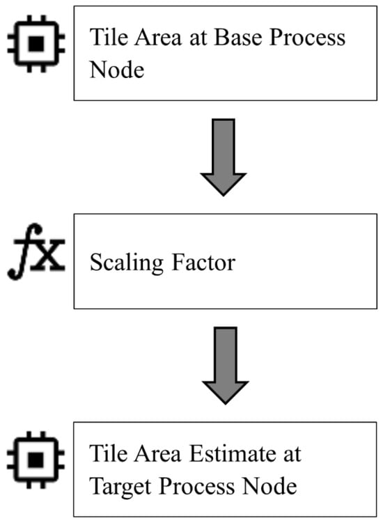
Figure 2.
FPGA tile area scaling across process nodes.
While the machine learning approach discussed in previous work can achieve high accuracy when sufficient training data is available, it requires a relatively large and technology-specific dataset and must be retrained for new process nodes. In contrast, the proposed scaling methodology does not require model training or large datasets and can generalize across nodes using only one reference layout. Although the machine learning approach offers flexibility and the ability to capture non-linear dependencies, it lacks cross-node generalization without significantly more training data.
The remainder of this section reviews common methodologies that can be used to estimate the area of FPGA tiles.
2.1. Direct Tile Design
One of the methods for determining the area of an FPGA tile is to design the tile. While this approach yields accurate results, it is highly time-consuming, particularly when exploring a large number of architectures that can potentially target specific application domains. Such an approach remains time-consuming, and computationally intensive, even when automated tools such as OpenFPGA [13], Fabulous [14], Princeton reconfigurable gate array (PRGA) [15], and others [16,17] are used. Such challenges make direct tile design unfeasible for the iterative exploration of FPGA architectures.
2.2. Minimum Width Transistor Area Model
In contrast to designing the FPGA tile to extract its area characteristics, the minimum width transistor area (MWTA) model estimates the area of an FPGA tile by summing the areas of the individual transistors within the tile. Although this approach circumvents the challenges associated with full tile design, previous work reports that such models introduce inaccuracies in area estimates of up to 50% [18,19,20,21,22,23,24,25]. This is because they do not account for layout optimization strategies such as diffusion and gating sharing. Moreover, the MWTA model assumes that the sizes of the transistors in the tile are predefined, thereby requiring users to determine the transistor sizes independently. Although tools such as circuit optimization for FPGA exploration (COFFE) have been proposed to address the transistor sizing problem, they are iterative and time-consuming, particularly when sweeping through large sets of FPGA architectural parameters [26,27].
2.3. Regression-Based Tile Area Estimation Models
Some FPGA tile area estimation methodologies utilize regression models to estimate the area of an FPGA tile based on the architectural parameters that are used to construct the tile [11,12]. While these approaches have shown reasonable prediction accuracies, their generalizability is limited because the experiments have been conducted using a single process node. This dependency restricts the direct applicability of such methodologies across different process nodes without the availability of a dataset that can be used to train the regression models. In this study, we extend these methodologies to enable FPGA tile area scaling across multiple process nodes.
2.4. Dennard Scaling
Dennard scaling is another approach that can be used to estimate FPGA tile area across process nodes [10]. According to this model, the area of transistors reduces proportionally to the square of their feature size as their sizes shrink. Although this approach is effective for earlier process nodes, the model’s accuracy declines at advanced nodes due to non-ideal scaling effects.
2.5. Scaling Factors
A previous study [9] proposed the use of constant scaling factors to estimate the implementation area of digital circuits across different semiconductor process nodes. These scaling factors were derived by analyzing the area of inverter-only circuits synthesized at various nodes and then extrapolating scaling ratios. Table 1 summarizes the scaling factors reported in the previous study [9] for transitions between the 130 nm, 45 nm, and 7 nm technology nodes. More specifically, the values in Table 1 represent the relative area scaling multipliers between target and base processes. For example, a value of in the first row indicates that a circuit implemented in 130 nm occupies approximately 110 times more area than the same circuit implemented in 7 nm. Similarly, moving from 45 nm to 7 nm corresponds to an area reduction factor of .

Table 1.
Scaling factors reported in a previous study [9].
While this approach is computationally efficient and conceptually appealing, we find that applying these scaling factors to synthesizable FPGA tile architectures leads to significant inaccuracies. Specifically, when scaling the area of all 1728 FPGA tile configurations in our dataset using the factors from [9], we observe maximum absolute percentage errors of up to 182%.
3. Methodology
Accurate estimation of FPGA tile area is critical for efficient FPGA architecture exploration. In this work, we leverage the scaling behavior of various standard cells and hierarchical blocks to develop a methodology for estimating how FPGA tile area changes across technology nodes. These components serve as the foundational references for understanding and modeling area scaling trends, thereby reducing design time and effort.
This section describes the experimental framework used in our analysis. First, we detail the FPGA tile architectures under study, including the key architectural parameters that define each configuration. Next, we outline the semiconductor process nodes and associated standard cell libraries that form the basis for cross-node comparisons. Finally, we present the methodology for dataset collection, which involves synthesizing a wide range of FPGA tile instances and extracting their area data. This dataset enables both the empirical analysis of the scaling behavior of synthesizable FPGA tiles across process nodes and the rigorous evaluation of the proposed area estimation approach.
3.1. FPGA Tile Architecture
As shown in Figure 3, the programmable logic portion of an FPGA is composed of several key components:
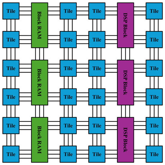
Figure 3.
Subsection of tile-based FPGA programmable logic fabric.
- Programmable tiles (Tile) that implement basic logic functionality.
- Block random-access memories (BRAMs) for data storage.
- Digital signal processing (DSP) blocks for arithmetic operations.
- A programmable routing network that connects all components using horizontal and vertical routing tracks.
These elements collectively define the computational and connectivity capabilities of the FPGA’s programmable logic. The architecture of an FPGA can be customized through a wide range of architectural parameters, which directly impact logic density, routing flexibility, performance, and power efficiency [28,29,30,31,32,33,34,35,36,37]. As such, selecting appropriate combinations of these parameters is therefore essential for developing efficient FPGA architectures.
As shown in Figure 4, a typical FPGA tile comprises the following elements:
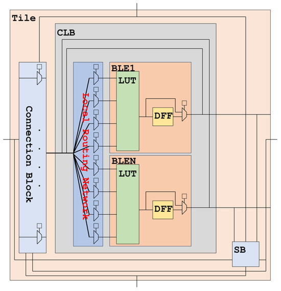
Figure 4.
FPGA tile.
- A lookup table (LUT)-based configurable logic block (CLB).
- Connection blocks (CBs) that provide programmable connectivity between the CLB and routing tracks.
- A switch block (SB) that enables programmable connections between vertical and horizontal routing channels.
Each of these subcomponents can be customized through architectural parameters, such as those listed in Table 2. These parameters include LUT size, number of LUTs, number of routing tracks, connection block flexibility, switch block topology, and segment lengths. The design space defined by these parameters is vast, and selecting the appropriate configurations is crucial for optimizing FPGA performance and area for a given application domain.
Table 2.
FPGA tile architectural parameters and explored ranges.
3.2. Standard Cell Libraries
The experimental research environment for this work leverages ASIC synthesis tools and open-source standard cell libraries for various process nodes. Table 3 lists the open-source standard cell design kits that are used in this work.
Table 3.
Process nodes and corresponding design kits.
The synthesizable FPGA tiles analyzed in this work are primarily constructed using 2-to-1 multiplexers (MUX2) and D-type flip-flops (DFFs). The MUX2 elements form the multiplexer trees within the tile, providing logic selection functionality for the LUTs, connection blocks, and switch blocks. The DFFs serve dual roles: they function as configuration memory to store programming bits and as output registers for the LUTs. Additional logic in the FPGA tile netlists support other functions such as clock distribution and reset control.
The implementation of MUX2 instances varies across standard cell libraries. Figure 5 presents post-synthesis netlists of MUX2 instances synthesized using the standard cell libraries and technology nodes listed in Table 2. As shown in the figure, the internal composition of the MUX2 instances differs between libraries. For example, the 130 nm standard cell library includes a dedicated MUX2 cell, whereas the 7 nm library lacks such a primitive, requiring synthesis tools to construct MUX2 functionality by combining an AND-OR standard cell with an inverter.
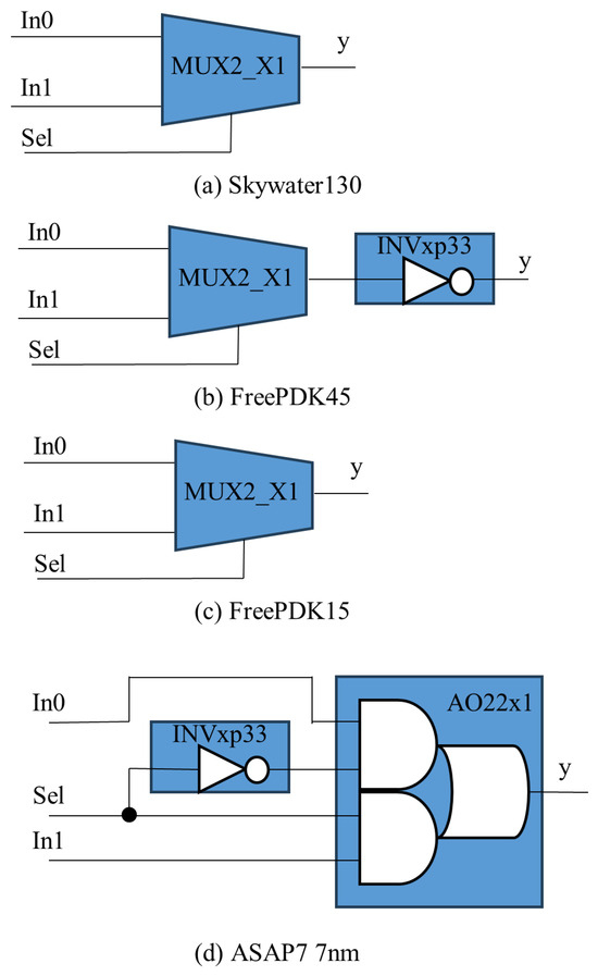
Figure 5.
Illustration of 2-to-1 multiplexer implementations using different standard cell libraries.
Non-uniformity in MUX2 implementation can also be observed within a single FPGA tile. Prior work has shown that the MUX2 instances in two basic logic elements (BLEs) within the same tile can exhibit structural differences depending on synthesis optimizations and local constraints [12].
These variations in MUX2 composition across process nodes and within individual tiles complicate traditional area estimation techniques that rely on summing the areas of constituent standard cells. To address this challenge, we adopt an empirical approach and analyze the synthesized area of complete FPGA tiles across various technology nodes. From these measurements, we extract scaling trends that can be used to derive scaling factors, which in turn enable the approximation of FPGA tile area at different process nodes without requiring component-level breakdowns.
3.3. Dataset Collection Methodology
A comprehensive dataset is essential for accurately analyzing the scaling behavior of synthesizable FPGA tiles across multiple process nodes. This dataset enables the study of scaling trends and serves as the foundation for validating the accuracy of the proposed area scaling methodology. To create the dataset, we develop an automated design and synthesis framework that generates FPGA tiles across a broad range of architectural parameters and process technologies. The overall dataset generation flow is illustrated in Figure 6.
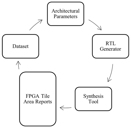
Figure 6.
Dataset collection methodology.
The dataset creation process begins by selecting a combination of architectural parameters, as listed in Table 2. These parameters are fed into a custom register transfer level (RTL) generator, which produces the corresponding Verilog description of the FPGA tile. The Verilog design is then synthesized using backend tools along with the appropriate standard cell libraries for the target process node. The synthesis process outputs netlists composed of standard cells and generates detailed synthesis reports, including area metrics.
After synthesis, the reports are automatically parsed to detect design issues such as timing violations or synthesis errors. If the design passes all checks, the area result is recorded in the dataset. To ensure broad coverage, this process is repeated across a diverse set of architectural configurations and process nodes.
The dataset compiled in this study contains 1728 FPGA tile instances, each representing a unique combination of architectural parameters synthesized at different process nodes. This dataset provides an empirical foundation for analyzing area scaling trends and evaluating the proposed area estimation methodology.
4. Results
The relationship between process node scaling and the resulting changes in FPGA tile area provides valuable insight into technology-driven design trends. By empirically analyzing these trends, we can formulate estimation models that generalize across nodes. To support this investigation, we synthesize a diverse set of 1728 FPGA tile architectures using four technology nodes: 130, 45, 15, and 7 nm. The resulting area data enables validation of the proposed methodology and the extraction of reliable scaling patterns to inform future FPGA fabric design.
The objectives of this section are as follows:
- To analyze trends in synthesizable FPGA tile area across process nodes.
- To formulate a scaling methodology based on empirical results for area estimation across process nodes.
- To derive scaling factors for approximating synthesizable FPGA tile area across process nodes.
- To evaluate the accuracy of the scaling methodology in terms of mean and maximum absolute percentage errors.
4.1. Scaling Trends
Previous studies on non-FPGA digital designs have demonstrated that circuit area can be approximated across semiconductor process nodes using constant scaling factors [9]. This study extends this concept to FPGA architectures, specifically synthesizable FPGA tiles. Through empirical analysis, we observe that the area of FPGA tiles can similarly be approximated across different technology nodes using constant scaling factors.
To illustrate this constant scaling behavior, Table 4 presents the measured area results for three representative FPGA architectures synthesized across multiple process nodes. To validate the use of constant scaling factors, the data shown in Table 4 is analyzed such that the area scaling between every pair of process nodes is captured as a ratio for each architecture, forming the basis of the scaling factors.
Table 4.
Example FPGA tile architectures and their corresponding areas across process nodes.
The derived scaling factors for each of the three example architectures are presented in Table 5, Table 6 and Table 7. Examination of these tables reveals that all three architectures follow similar scaling trends when transitioning between process nodes. For instance, when ARCH1 is scaled from 45 nm to 15 nm, the corresponding scaling factor is approximately . Under the same technology transition, comparable scaling behavior is observed for ARCH2 and ARCH3. Most importantly, we find that these scaling trends are not limited to the representative examples. Across the complete dataset of 1728 FPGA tile architectures, the scaling factors remain consistent and predictable when transitioning between the studied process nodes.
Table 5.
ARCH1 scaling factors between base and target processes.
Table 6.
ARCH2 scaling factors between base and target processes.
Table 7.
ARCH3 scaling factors between base and target processes.
Table 8 summarizes the variability in scaling factors across the entire architectural design space. Specifically, it reports the standard deviation of scaling factors derived from all 1728 architectures relative to the mean. As shown, the standard deviation reaches a maximum of 2.68%. This level of variability suggests that, despite some deviations, using constant scaling factors offers reasonable accuracy for estimating the area of synthesizable FPGA tiles across different semiconductor process nodes. This consistency supports the general applicability of constant scaling factors for cross-node area estimation in FPGA fabric design.
Table 8.
Standard deviation of the scaling factors for all 1728 architectures.
To further investigate the accuracy of using constant scaling factors to scale the area of synthesizable FPGA architectures between process nodes, we use the scaling factors that are derived from ARCH1 to scale the area of all 1728 architectures in the dataset. Figure 7 illustrates the mean absolute percentage error (Mean APE) and the maximum absolute percentage error (Max APE) when scaling all 1728 architectures between the process nodes. As shown, the mean absolute percentage error is below 1% and the maximum absolute percentage error is below 10%.
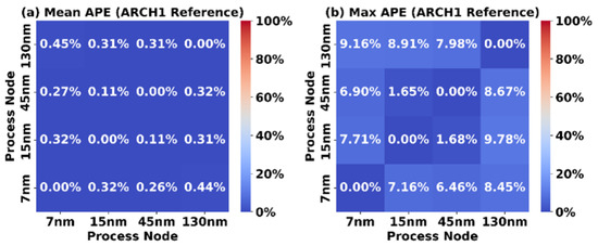
Figure 7.
Accuracy of scaling all 1728 FPGA tile architectures using the ARCH1 scaling factors. (a) Mean absolute percentage error (Mean APE). (b) Maximum absolute percentage error (Max APE). The Mean APE and Max APE reach approximately 0.45% and 9.78%, respectively, when using the process-dependent ARCH1 tile area as the scaling reference for all 1728 FPGA tile architectures.
4.2. Formulation
Equation (1) summarizes the process node scaling methodology:
where,
- represents the area of an FPGA tile that is synthesized at a specific process node.
- represents the area of a reference block that is synthesized at a specific process node.
- represents the scaling factor. The scaling factor is a function of the area of the reference block at the base and target process nodes.
As stated in (1), the area of a synthesizable FPGA tile synthesized using a target process node , denoted as , can be estimated by scaling the area of an FPGA tile at a base process , denoted as , by a scaling factor . The scaling factor is a function of the area of a reference block when synthesized using both the base process and the target process . This approach leverages the relative scaling of synthesizable FPGA tiles and other hierarchical blocks across process technologies to derive scaling factors that can be used to scale the area of an FPGA tile between process nodes.
4.3. Alternative Scaling References
The scaling factor quantifies the change in the area of a synthesizable FPGA tile as the process technology varies. This section explores the use of alternative reference blocks to derive . These references may not always offer greater accuracy compared to using the full tile area as a reference. However, they present a practical advantage: their area values can be directly extracted from standard cell libraries. As a result, these reference blocks can serve as effective substitutes when tile-level area data is unavailable or difficult to obtain.
Table 9 lists the standard cells and hierarchical blocks examined in this study as potential alternative scaling references. These include a 2-input NAND gate (NAND2), a DFF, a 2-to-1 multiplexer (MUX2), and a 4-to-1 multiplexer (MUX4). These components were chosen for their relevance to the underlying logic structures within the synthesizable FPGA tiles studied in this work.
Table 9.
Reference block areas across different process nodes.
Figure 8 shows the mean absolute percentage error (Mean APE) and maximum absolute percentage error (Max APE) as a result of using a NAND2 standard cell as a scaling reference to estimate the area of all 1728 synthesizable FPGA tiles across the different process nodes. While NAND2 cells do not dominate the tile netlists, the results show that this method achieves a Mean APE of less than 5% and a Max APE of approximately 24%, demonstrating moderate accuracy.
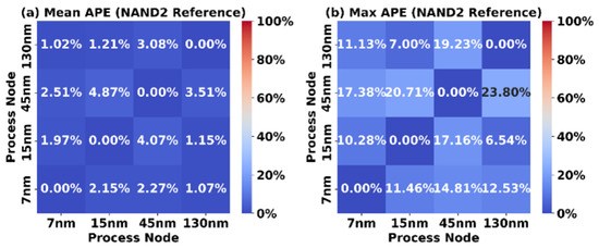
Figure 8.
Accuracy of NAND2 reference scaling.
In comparison, the MUX2-based scaling reference yields greater accuracy. As shown in Figure 9, using a MUX2 as the reference results in a Mean APE below 2% and a Max APE around 13%. This improvement is expected, as the FPGA tile netlists that are studied in this work heavily feature MUX2 and DFF instances, making the MUX2 a more representative reference.
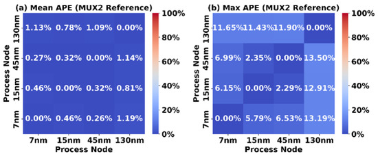
Figure 9.
Accuracy of MUX2 reference scaling.
Similarly, Figure 10 illustrates the results when a DFF standard cell is used as the scaling reference. This method achieves a Mean APE below 3% and a Max APE of approximately 12%, further validating the use of DFFs due to their prevalence in the synthesized tile architectures.
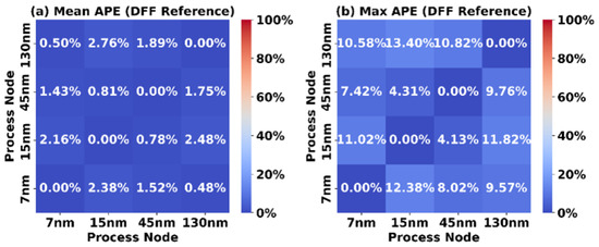
Figure 10.
Accuracy of DFF reference scaling.
Finally, Figure 11 shows the error metrics when using a MUX4 reference block. The Mean APE and Max APE values are comparable to those of the MUX2 reference. This is because an unflattened MUX4 is logically and structurally composed of three MUX2 units, resulting in scaling behavior similar to that of a MUX2.
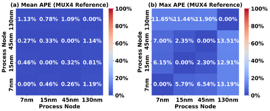
Figure 11.
Accuracy of MUX4 reference scaling.
4.4. Accuracy
Table 10 presents the mean of the base–target process node scaling factors for all 1728 FPGA architectures examined in this study. As noted earlier, the scaling factor may deviate from the average by up to 2.68% for any given base–target process node pair. To evaluate the accuracy of these scaling factors, we measure both the mean absolute percentage error (Mean APE) and the maximum absolute percentage error (Max APE), as illustrated in Figure 12.
Table 10.
Mean of tile-level scaling factors for all 1728 architectures across target and base processes.
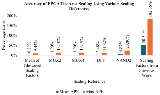
Figure 12.
Accuracy of FPGA tile area scaling using various scaling references and scaling factors from previous work [9].
Figure 12 compares the scaling factors listed in Table 10 with several alternatives: those reported in [9], and those derived from the MUX2, MUX4, DFF, and NAND2 standard cells (as discussed in this work). The analysis shows that using the area of an FPGA tile as the scaling reference yields the lowest mean and maximum absolute percentage errors. Scaling references derived from MUX and DFF cells result in slightly higher errors, while the NAND2 scaling reference and the scaling factors from [9] produce maximum absolute percentage errors of 23.8% and 182%, respectively.
The results show that synthesizable FPGA tile area scales consistently across process node pairs. Notably, if one FPGA tile area scales by a given factor between two process nodes, then the same factor can reliably approximate the scaling of all FPGA tile architectures between those nodes. Multiplexers and DFFs constitute the majority of the FPGA tile area in the architectures studied; therefore, their scaling behavior closely matches that of entire FPGA tiles, and scaling factors derived from these components can serve as accurate references for estimating FPGA tile area changes across process nodes.
5. Conclusions
The findings in this work indicate that the area of a synthesizable FPGA tile can be effectively modeled using constant scaling factors when scaled across semiconductor process nodes. The scaling factors can be derived from reference blocks such as the area of an FPGA tile, MUX2, MUX4 and DFF instances. Such a scaling methodology can achieve a maximum absolute percentage error of less than 10% when measured over a range of 1728 synthesizable FPGA architectures synthesized using the 130 nm, 45 nm, 15 nm and 7 nm process nodes. This methodology can be used to accelerate the early stages of the FPGA architecture exploration process by providing a reliable means of scaling the area of synthesizable FPGA tiles across process nodes without the need for full synthesis at each process node.
The proposed scaling methodology has been validated across four open-source process nodes, ranging from a planar CMOS-based 130 nm node to a FinFET-based 7 nm technology. The ability to obtain accurate scaling results across this wide technological span demonstrates that the method effectively models front-end scaling effects, which primarily govern standard-cell area and logic density. Nonetheless, the model does not explicitly account for back-end-of-line (BEOL) effects such as interconnect parasitics and metal stack variations. These factors may introduce additional variability when extending the methodology to more advanced technology nodes; therefore, future work merits investigating the incorporation of BEOL effects to further enhance the model’s predictive accuracy.
Author Contributions
Writing—original draft preparation, M.A.-Q.; supervision, A.Y. All authors have read and agreed to the published version of the manuscript.
Funding
This research received no external funding.
Data Availability Statement
The data supporting the conclusions of this article will be made available by the authors on request.
Conflicts of Interest
The authors declare no conflicts of interest.
Abbreviations
The following abbreviations are used in this manuscript:
| APE | Absolute Percentage Error |
| ASIC | Application Specific Integrated Circuit |
| BEOL | Back End of Line |
| BLE | Basic Logic Element |
| BRAM | Block Random Access Memory |
| CB | Connection Block |
| CLB | Configurable Logic Block |
| COFFE | Circuit Optimization for FPGA Exploration |
| DSP | Digital Signal Processing |
| DFF | D-type Flip Flop |
| FinFET | Fin Field Effect Transistor |
| FPGA | Field Programmable Gate Array |
| LUT | Lookup Table |
| MUX2 | 2-to-1 Multiplexer |
| MUX4 | 4-to-1 Multiplexer |
| MWTA | Minimum Width Transistor Area |
| PRGA | Princeton Reconfigurable Gate Array |
| RTL | Register Transfer Level |
| SB | Switch Block |
| XGBoost | eXtreme Gradient Boosting |
References
- Ajayi, T.; Blaauw, D.; Chan, T.B.; Cheng, C.K.; Chhabria, V.A.; Choo, D.K.; Coltella, M.; Dobre, S.; Dreslinski, R.; Fogaça, M.; et al. OpenROAD: Toward a Self-Driving, Open-Source Digital Layout Implementation Tool Chain. In Proceedings of the GOMACTech, Albuquerque, NM, USA, 25–28 March 2019; pp. 1105–1110. [Google Scholar]
- Ajayi, T.; Chhabria, V.A.; Fogaça, M.; Hashemi, S.; Hosny, A.; Kahng, A.B.; Kim, M.; Lee, J.; Mallappa, U.; Neseem, M.; et al. Toward an Open-Source Digital Flow: First Learnings from the OpenROAD Project. In Proceedings of the 56th Annual Design Automation Conference (DAC 2019), Las Vegas, NV, USA, 2–6 June 2019; pp. 1–4. [Google Scholar]
- Shalan, M.; Edwards, T. Building OpenLANE: A 130 nm OpenROAD-based Tapeout-Proven Flow: Invited Paper. In Proceedings of the 2020 IEEE/ACM International Conference on Computer-Aided Design (ICCAD), San Diego, CA, USA, 2–5 November 2020; pp. 1–6. [Google Scholar] [CrossRef]
- Foundry, S.T. SkyWater 130 nm Process Design Kit (PDK). 2020. Available online: https://skywater-pdk.readthedocs.io/en/main/ (accessed on 15 November 2025).
- Betz, V.; Rose, J. VPR: A new packing, placement and routing tool for FPGA research. Field-Program. Log. Appl. FPL. Lect. Notes Comput. Sci. 1997, 1304, 213–222. [Google Scholar] [CrossRef]
- Luu, J.; Kuon, I.; Jamieson, P.; Campbell, T.; Ye, A.; Fang, W.M.; Kent, K.; Rose, J. VPR 5.0: FPGA CAD and Architecture Exploration Tools with Single-Driver Routing, Heterogeneity and Process Scaling. ACM Trans. Reconfigurable Technol. Syst. 2011, 4, 1–23. [Google Scholar] [CrossRef]
- Murray, K.E.; Petelin, O.; Zhong, S.; Wang, J.M.; Eldafrawy, M.; Legault, J.P.; Sha, E.; Graham, A.G.; Wu, J.; Walker, M.J.P.; et al. VTR 8: High-performance CAD and Customizable FPGA Architecture Modelling. ACM Trans. Reconfigurable Technol. Syst. 2020, 13, 1–55. [Google Scholar] [CrossRef]
- Elgammal, M.A.; Mohaghegh, A.; Shahrouz, S.G.; Mahmoudi, F.; Koşar, F.; Talaei, K.; Fife, J.; Khadivi, D.; Murray, K.; Boutros, A.; et al. VTR 9: Open-Source CAD for Fabric and Beyond FPGA Architecture Exploration. ACM Trans. Reconfigurable Technol. Syst. 2025, 18, 1–53. [Google Scholar] [CrossRef]
- Stillmaker, A.; Baas, B. Scaling equations for the accurate prediction of CMOS device performance from 180 nm to 7 nm. Integration 2017, 58, 74–81. [Google Scholar] [CrossRef]
- Sarangi, S.; Baas, B. DeepScaleTool: A Tool for the Accurate Estimation of Technology Scaling in the Deep-Submicron Era. In Proceedings of the IEEE International Symposium on Circuits and Systems Proceedings, Daegu, Republic of Korea, 23–26 May 2021; IEEE: Piscataway, NJ, USA, 2021; pp. 1–5. [Google Scholar]
- Al-Qawasmi, M.; Ye, A.G. Estimating Post-Synthesis Area, Delay, and Leakage Power of Standard Cell Based FPGA Tiles. In Proceedings of the 2023 IEEE Canadian Conference on Electrical and Computer Engineering (CCECE), Regina, SK, Canada, 24–27 September 2023; pp. 117–123. [Google Scholar] [CrossRef]
- Al-Qawasmi, M.; Ye, A.G. A Regression-Based Approach Towards Estimating the Area, Delay and Leakage Power of Synthesizable FPGA Tiles. In Proceedings of the 2024 International Conference on Field Programmable Technology (ICFPT), Sydney, Australia, 10–12 December 2024; pp. 1–10. [Google Scholar] [CrossRef]
- Tang, X.; Giacomin, E.; Chauviere, B.; Alacchi, A.; Gaillardon, P.E. OpenFPGA: An Open-Source Framework for Agile Prototyping Customizable FPGAs. IEEE Micro 2020, 40, 41–48. [Google Scholar] [CrossRef]
- Koch, D.; Dao, N.; Healy, B.; Yu, J.; Attwood, A. FABulous: An Embedded FPGA Framework. In Proceedings of the 2021 ACM/SIGDA International Symposium on Field-Programmable Gate Arrays, Virtual, 28 February–2 March 2021; Association for Computing Machinery: New York, NY, USA, 2021; pp. 45–56. [Google Scholar] [CrossRef]
- Li, A.; Wentzlaff, D. PRGA: An Open-Source FPGA Research and Prototyping Framework. In Proceedings of the 2021 ACM/SIGDA International Symposium on Field-Programmable Gate Arrays, Virtual, 28 February–2 March 2021; Association for Computing Machinery: New York, NY, USA, 2021; pp. 127–137. [Google Scholar] [CrossRef]
- Grady, B.; Anderson, J.H. Synthesizable Heterogeneous FPGA Fabrics. In Proceedings of the 2018 International Conference on Field-Programmable Technology (FPT), Naha, Japan, 10–14 December 2018; pp. 222–229. [Google Scholar] [CrossRef]
- Grady, B.; Anderson, J.H. Physical Design Considerations for Synthesizable Standard-Cell-Based FPGAs. In Proceedings of the 10th International Symposium on Highly-Efficient Accelerators and Reconfigurable Technologies, Nagasaki, Japan, 6–7 June 2019; Association for Computing Machinery: New York, NY, USA, 2019. [Google Scholar] [CrossRef]
- Khan, F.F.; Ye, A. Measuring the Accuracy of Minimum Width Transistor Area in Estimating FPGA Layout Area. In Proceedings of the 2015 IEEE 23rd Annual International Symposium on Field-Programmable Custom Computing Machines, Vancouver, BC, Canada, 3–5 May 2015; pp. 223–226. [Google Scholar] [CrossRef]
- Khan, F.F.; Ye, A. An evaluation on the accuracy of the minimum width transistor area models in ranking the layout area of FPGA architectures. In Proceedings of the 2016 26th International Conference on Field Programmable Logic and Applications (FPL), Lausanne, Switzerland, 29 August–2 September 2016; pp. 1–11. [Google Scholar] [CrossRef]
- Khan, F.F.; Ye, A. A study on the accuracy of minimum width transistor area in estimating FPGA layout area. Microprocess. Microsyst. 2017, 52, 287–298. [Google Scholar] [CrossRef]
- Khan, F.; Ye, A. An Evaluation on the Accuracy of the Minimum-Width Transistor Area Models in Ranking the Layout Area of FPGA Architectures. ACM Trans. Reconfigurable Technol. Syst. 2018, 11, 1–23. [Google Scholar] [CrossRef]
- Al-Qawasmi, M.; Ye, A.G. An Investigation of the Accuracy of the VPR and COFFE Area Models in Predicting the Layout Area of FPGA Lookup Tables. In Proceedings of the 2020 SoutheastCon, Raleigh, NC, USA, 12–15 March 2020; pp. 1–9. [Google Scholar] [CrossRef]
- Sani, S.R.; Khan, F.F.; Razzaq, A.; Ye, A. Measuring the Accuracy of Layout Area Estimation Models of Tile-Based FPGAs in FinFET Technology. In Proceedings of the 2020 30th International Conference on Field-Programmable Logic and Applications (FPL), Gothenburg, Sweden, 31 August–4 September 2020; pp. 214–219. [Google Scholar] [CrossRef]
- Rostami-Sani, S.; Ye, A. Measuring the effect of track count and wire segment length on the layout area of switch blocks for tile-based FPGAs. Microprocess. Microsyst. 2022, 92, 104563. [Google Scholar] [CrossRef]
- Sani, S.R.; Ye, A. Evaluating the Impact of Using Multiple-Metal Layers on the Layout Area of Switch Blocks for Tile-Based FPGAs in FinFET 7 nm. ACM Trans. Reconfigurable Technol. Syst. 2024, 17, 1–29. [Google Scholar] [CrossRef]
- Chiasson, C.; Betz, V. COFFE: Fully-automated transistor sizing for FPGAs. In Proceedings of the 2013 International Conference on Field-Programmable Technology (FPT), Kyoto, Japan, 9–11 December 2013; pp. 34–41. [Google Scholar] [CrossRef]
- Yazdanshenas, S.; Betz, V. COFFE 2: Automatic Modelling and Optimization of Complex and Heterogeneous FPGA Architectures. ACM Trans. Reconfigurable Technol. Syst. 2019, 12, 1–27. [Google Scholar] [CrossRef]
- Rose, J.; Francis, R.J.; Lewis, D.; Chow, P. Architecture of field-programmable gate arrays: The effect of logic block functionality on area efficiency. IEEE J. Solid-State Circuits 1990, 25, 1217–1225. [Google Scholar] [CrossRef]
- Singh, S.; Rose, J.; Chow, P.; Lewis, D. The effect of logic block architecture on FPGA performance. IEEE J. Solid-State Circuits 1992, 27, 281–287. [Google Scholar] [CrossRef]
- Gamal, A.E.; Kouloheris, J.L. FPGA performance versus cell granularity. In Proceedings of the IEEE Custom Integrated Circuits Conference, Boston, MA, USA, 3–6 May 1992; pp. 1–4. [Google Scholar]
- Hill, D.; Woo, N.S. The benefits of flexibility in lookup table-based FPGAs. IEEE Trans. Comput.-Aided Des. Integr. Circuits Syst. 1993, 12, 349–353. [Google Scholar] [CrossRef]
- Betz, V.; Rose, J. Cluster-based logic blocks for FPGAs: Area-efficiency vs. input sharing and size. In Proceedings of the CICC 97—Custom Integrated Circuits Conference, Denver, CO, USA, 5–8 May 1997; pp. 551–554. [Google Scholar] [CrossRef]
- Betz, V.; Rose, J. How much logic should go in an FPGA logic block. IEEE Des. Test Comput. 1998, 15, 10–15. [Google Scholar] [CrossRef]
- Marquardt, A.; Betz, V.; Rose, J. Speed and area tradeoffs in cluster-based FPGA architectures. IEEE Trans. Very Large Scale Integr. (VLSI) Syst. 2000, 8, 84–93. [Google Scholar] [CrossRef]
- Ahmed, E.; Rose, J. The Effect of LUT and Cluster Size on Deep-Submicron FPGA Performance and Density. IEEE Trans. Very Large Scale Integr. (VLSI) Syst. 2004, 12, 288–298. [Google Scholar] [CrossRef]
- Zgheib, G.; Lortkipanidze, M.; Owaida, M.; Novo, D.; Ienne, P. FPRESSO: Enabling Express Transistor-Level Exploration of FPGA Architectures. In Proceedings of the 2016 ACM/SIGDA International Symposium on Field-Programmable Gate Arrays. Association for Computing Machinery, Monterey, CA, USA, 21–23 February 2016; pp. 80–89. [Google Scholar] [CrossRef]
- Zgheib, G.; Ienne, P. Evaluating FPGA clusters under wide ranges of design parameters. In Proceedings of the 2017 27th International Conference on Field Programmable Logic and Applications (FPL), Ghent, Belgium, 4–8 September 2017; pp. 1–8. [Google Scholar] [CrossRef]
- Stine, J.E.; Castellanos, I.; Wood, M.; Henson, J.; Love, F.; Davis, W.R.; Franzon, P.D.; Bucher, M.; Basavarajaiah, S.; Oh, J.; et al. FreePDK: An Open-Source Variation-Aware Design Kit. In Proceedings of the 2007 IEEE International Conference on Microelectronic Systems Education (MSE’07), San Diego, CA, USA, 3–4 June 2007; pp. 173–174. [Google Scholar] [CrossRef]
- Bhanushali, K.; Davis, W.R. FreePDK15: An Open-Source Predictive Process Design Kit for 15 nm FinFET Technology. In Proceedings of the 2015 Symposium on International Symposium on Physical Design. Association for Computing Machinery, Monterey, CA, USA, 29 March–1 April 2015; pp. 165–170. [Google Scholar] [CrossRef]
- Clark, L.T.; Vashishtha, V.; Shifren, L.; Gujja, A.; Sinha, S.; Cline, B.; Ramamurthy, C.; Yeric, G. ASAP7: A 7-nm finFET predictive process design kit. Microelectron. J. 2016, 53, 105–115. [Google Scholar] [CrossRef]
- Clark, L.T.; Vashishtha, V.; Harris, D.M.; Dietrich, S.; Wang, Z. Design flows and collateral for the ASAP7 7 nm FinFET predictive process design kit. In Proceedings of the 2017 IEEE International Conference on Microelectronic Systems Education (MSE), Lake Louise, AB, Canada, 11–12 May 2017; pp. 1–4. [Google Scholar] [CrossRef]
- Vashishtha, V.; Vangala, M.; Clark, L.T. ASAP7 predictive design kit development and cell design technology co-optimization: Invited paper. In Proceedings of the 2017 IEEE/ACM International Conference on Computer-Aided Design (ICCAD), Irvine, CA, USA, 13–16 November 2017; pp. 992–998. [Google Scholar] [CrossRef]


Disclaimer/Publisher’s Note: The statements, opinions and data contained in all publications are solely those of the individual author(s) and contributor(s) and not of MDPI and/or the editor(s). MDPI and/or the editor(s) disclaim responsibility for any injury to people or property resulting from any ideas, methods, instructions or products referred to in the content. |
© 2025 by the authors. Licensee MDPI, Basel, Switzerland. This article is an open access article distributed under the terms and conditions of the Creative Commons Attribution (CC BY) license (https://creativecommons.org/licenses/by/4.0/).