1. Introduction
With the continuous scaling of design rules, parasitic components in IC layouts exert an increasingly significant influence on integrated circuit (IC) behavior, including transient response and timing. In this work, parasitic components refer to parasitic capacitances and resistances associated with interconnect layers, such as polysilicon and metal layers.
An IC layout can be represented as a set of active and passive components—MOS and bipolar transistors, resistors, capacitors, and others—described in the foundry’s LVS (Layout Versus Schematic) extraction rules. LVS rules are applied both for verifying the correspondence between the layout and the schematic circuit and for generating netlists for simulation purposes, e.g., for SPICE simulators. In conventional LVS extraction rules, the connection of device pins is performed via interconnect layers that are assumed to have zero resistance and zero capacitance.
In modern PDK-based flows, core device models (MOS, RES, CAP, DIO, BIP, IND) and layout-extracted parasitic elements are coordinated through LVS/LPE options, model flags, and extraction switches in order to avoid both the omission and double counting of parasitic components. Therefore, the proposed method focuses on interconnect-related parasitic R/C components and assumes consistency with the foundry-qualified LVS rule deck and the corresponding device-model configuration.
Built-in devices are defined in the foundry process specification and LVS extraction rules, together with their specific device layers and names. The number of such devices varies widely across technologies, from several dozen to several thousand. Parasitic extraction becomes especially important when built-in devices cannot be excluded from the extraction process and the resulting netlist must remain fully consistent with the schematic representation, unlike in certain simplified approaches
2. Related Work and Positioning of the Proposed Flow
This section positions the proposed methodology relative to the existing parasitic-extraction and RC-reduction approaches.
Parasitic extraction is commonly addressed by two main classes of methods: numerical field-solver-based approaches and rule-based extraction flows. Numerical methods, including finite-difference, finite-element, boundary-element, method-of-moments, and floating-random-walk techniques, can provide high local accuracy for 2D, 2.5D, and 3D interconnect configurations [
1,
2,
3]. However, their direct use for large full-chip layouts is limited by runtime, meshing complexity, and the need for detailed boundary-condition setup. Rule-based parasitic extraction is widely used in industrial post-layout verification flows because it can be integrated with foundry-qualified design rules, LVS rule decks, and Process Design Kits (PDKs) [
4]. Such methods combine geometric layout operations with process-dependent parameters, including sheet resistance, contact/via resistance, conductor thickness, dielectric thickness, and layer-stack information. Therefore, rule-based extraction is not intended to replace field solvers in terms of local electromagnetic accuracy; rather, it provides a scalable engineering compromise between accuracy, runtime, and compatibility with production design flows. Recent work on parasitic resistance extraction [
5] and RC-network reduction [
6,
7,
8,
9,
10] has focused on improving scalability and reducing post-layout simulation cost. Image-processing-based resistance extraction has been proposed for deriving resistance networks from layout data, while model-order-reduction techniques reduce the number of internal nodes and circuit equations in large extracted RC networks.
In parallel, recent studies have explored alternative approaches for accelerating parasitic extraction. Machine-learning-assisted capacitance extraction methods based on DNN, CNN, and GNN models have been proposed to predict interconnect capacitance matrices or chip-scale capacitance values using field-solver-generated or pre-characterized datasets [
11,
12,
13,
14,
15]. These methods demonstrate the relevance of data-driven extraction, but they remain complementary to rule-deck-based flows because they require training data and separate validation. Classical layout-to-circuit extractors and timing-oriented VLSI interconnect extraction methods also demonstrate the importance of scalable geometry-driven extraction for simulation-oriented design flows [
16,
17]. The present work is positioned within the class of rule-based LVS-driven parasitic RC extraction methodologies. Its objective is not compact-model parameter extraction for semiconductor devices, such as BSIM or HiCuM model fitting, but layout-driven parasitic R/C extraction for post-layout SPICE simulation. The proposed flow uses foundry-qualified LVS rule-deck information and extends it with the rule-based extraction of interconnect resistances, contact and via resistances, gate resistance, and parasitic capacitances. In addition, a compact RC-merging procedure based on π-equivalent capacitance models is introduced to combine separately extracted resistance and capacitance networks into a simulation-ready netlist. The main distinction of the proposed approach is that it operates directly within the LVS-rule environment and therefore preserves consistency with the connectivity, device recognition, and layer definitions already used for physical verification. The method is geometry-driven in implementation but physically parameterized by process-dependent electrical and dielectric data from the target technology. This enables the scalable post-layout simulation of large planar CMOS layouts, provided that technology-dependent parameters are updated and requalified for the target PDK. The above positioning of the proposed flow relative to numerical field solvers, rule-based PEX, ML/DL-assisted extraction, and RC model-order reduction is summarized in
Table 1.
The method was implemented in the SmartLVS tool, which uses a dedicated command subset known as the PoWerful Ruledeck Language (PWRL), as an example of an LVS-rule-based environment [
18]. The methodology supports layouts containing a single poly/gate layer and up to seven metal layers (M1–M7), which represent the standard interconnect stack in typical IC designs for mature process nodes. The approach can also be extended to more advanced technologies incorporating up to M8–M12 metal layers with only a modest impact on extraction performance.
A practical advantage of the proposed flow is that it is based on foundry-certified LVS extraction rules and can be applied directly. LVS is used to compare the physical layout with the original circuit description (schematic netlist), and the proposed flow extracts the required information from the same sources. No standalone rule deck is required; instead, the parasitic-extraction section is included as an external file. The relevant design rules are defined in the Process Specification (PS) and Design Rules Manual (DRM) for the target foundry technology. The tool executes a PWRL-based rule deck describing active devices, parasitic capacitances, and connectivity, and produces a SPICE-compatible netlist ready for immediate use in SPICE simulations.
For parasitic resistance and capacitance extraction, only the interconnect regions used for electrical connections in LVS extraction rules are considered, namely polysilicon and metal interconnects. Their layer names can be identified directly from the foundry LVS rules. For example, contacts to built-in resistors can be determined through the metal and polysilicon layers defined in the LVS rules, which serve as interconnect buses linking built-in devices. In most cases, this approach provides correct results, as confirmed by testing across numerous rule decks from different foundries. In the simplest parasitic-resistance extraction treatment, all polysilicon and metal interconnect lines are decomposed into horizontal and vertical segments and extracted separately.
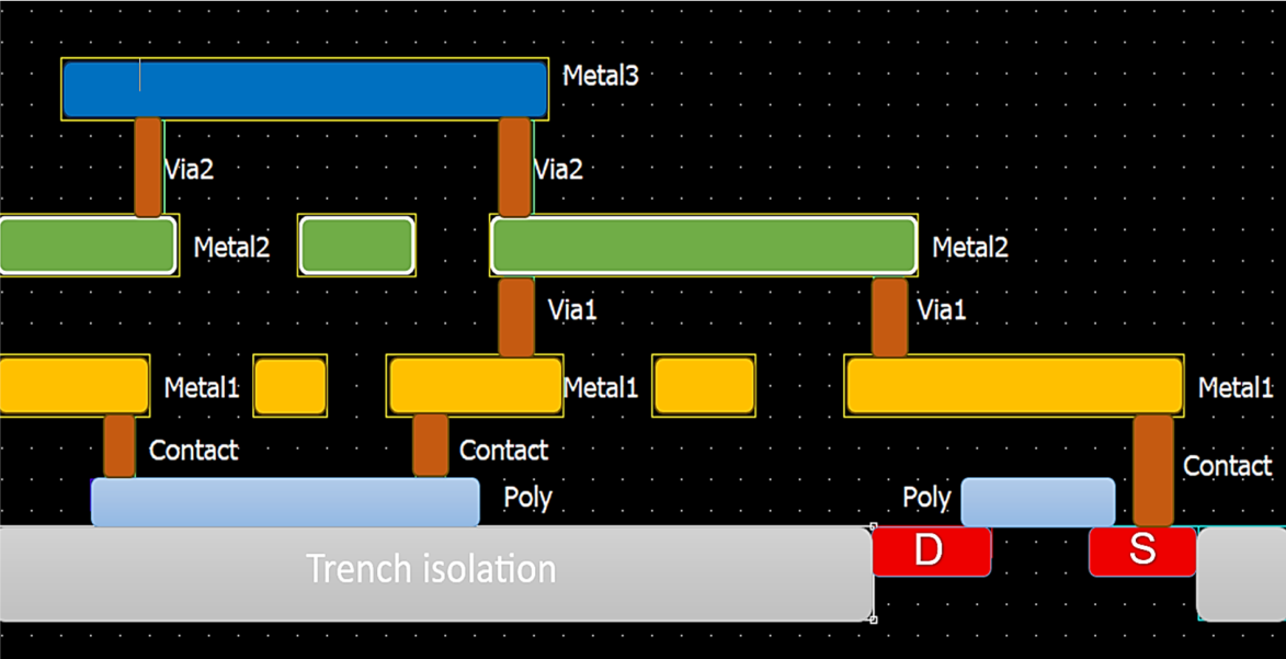
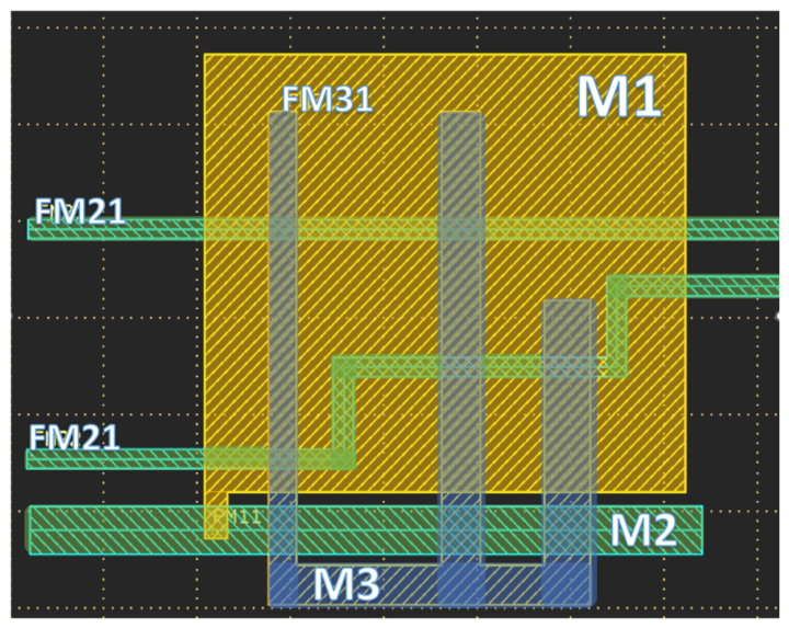
A schematic of the conventional metal stack for three metal layers (M1–M3) plus polysilicon is shown in
Figure 1, which also illustrates M1 contacts to polysilicon (“contact”) and inter-metal connections (vias). It is essential to extract the resistances of these elements because their contribution is not negligible. Because the process specifications and design-rule manuals used in this work are confidential, the foundries are anonymized as Fab1–Fab3. Numerical process parameters quoted below are representative process-specific values taken from confidential technology documentation and are used only to illustrate the relative magnitude of the corresponding parasitic effects. They should not be interpreted as universal constants for a given technology node. For the representative confidential 130–180 nm planar CMOS process data used in this work, the polysilicon-contact resistance is in the range of approximately 10–15 Ω. For the same process family, a representative M1 sheet resistance of approximately 0.1 Ω/□ was used. This contact resistance is therefore comparable to the resistance of a minimum-width 0.16 μm M1 line segment with a length of approximately 16–24 μm.
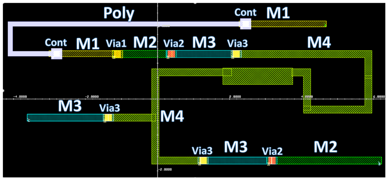
Since the method relies on a decomposition of interconnect polygons into horizontal and vertical components, it enables the robust detection of vias, contacts, and inter-metal transitions.
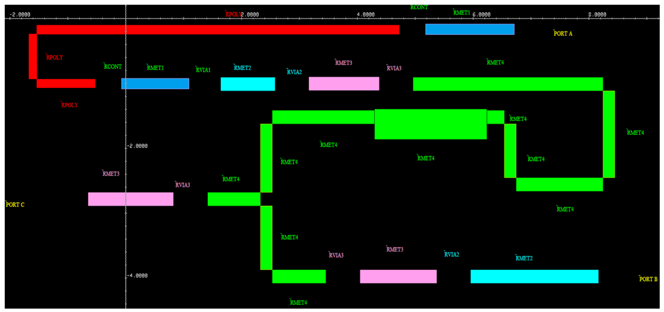
Figure 2 illustrates an example of such a test structure for the specific Fab1 180 nm CMOS foundry process, representing the sequential connection of poly, M1–M4 layers, contacts, and vias used to validate the extraction rules. The resulting parasitic-resistance polygons derived from the transformation steps are shown in
Figure 3, while
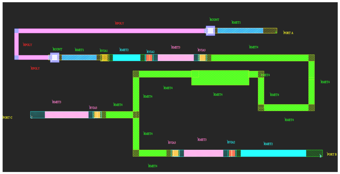
Figure 4 presents the combined layout view in which original interconnect shapes are overlaid with the extracted parasitic elements.
3. Methodology of Extraction and Accuracy Comparison
The following discussion illustrates examples of logical layer-processing operations in an LVS extraction rule file. The parasitic-resistance extraction method does not use a hierarchical approach; instead, it operates on a flat layout representation.
Although the extraction is implemented through rule-based geometric operations, the extracted quantities are not arbitrary geometric markers. Resistance values are derived from physical sheet, contact, and via resistance parameters provided by the PDK or DRM, while capacitance-related quantities depend on conductor overlap, spacing, width, dielectric thickness, and layer-stack configuration. Thus, the method is geometry-driven in implementation but physically parameterized by process-dependent electrical and dielectric data.
As an example, we present equations for computing polygons that define the resistances of horizontal interconnect buses in the M2 layer.
During the layout processing stage, text labels associated with interconnect layers may be transferred to newly formed resistive layers and thus lost. To prevent this, special layers, denoted as NRi, are generated. These NRi layers are created exclusively for top-level labels, ensuring the preservation of connectivity and proper association between resistive elements and their corresponding nets:
Here, the symbol “
$” denotes a PWRL command, while “%” denotes a variable value defined in a separate section of the LVS rule deck. The layer TxtM2 represents a text label associated with the M2 layer. The value of RTxtMi should be slightly larger than the size of a contact or via, yet smaller than the minimum spacing of the corresponding metal layer, in order to avoid overlapping with adjacent interconnects.
To ensure proper connectivity of the transformed layout when parasitic resistors are included, it is necessary to remove segments of the interconnect buses located within the contact and via areas.
Here, the last digit in the %Rvia2 variable must fall outside or below the design-grid resolution to avoid accidental contact with adjacent interconnects and prevent connectivity loss. For example, with a design grid of 0.005 μm, the final “m” digit should correspond to a value satisfying 0.005 < m < 0.01 or 0 < m < 0.005.
At this stage, the M2 interconnect buses can be transformed for the extraction of parasitic resistances.
Here, met2com is the M2 layer used for interconnections. For interconnect buses, rectangular polygons formed by parallel segments are detected as their edges. The term “parallel” refers to vertical and horizontal interconnect lines, although lines oriented at 45 degrees or at another angle may also be included if required.
At the junction of horizontal and vertical interconnect segments, no resistive layer is generated to maintain connectivity through the conductive layers. The length of a resistive segment with a constant width is limited only by the distance between contacts or by the branching/bending point of the bus.
The maximum width of conductive interconnect buses used in parasitic resistance extraction depends on the specific design rules of the process node and is defined by the corresponding variable values assigned to each conductive layer in LVS extraction rules.
Equation (4) defines the edges of horizontal conductive layers, with the length reduced by 0.005 μm. This reduction prevents the formation of a resistive layer between adjacent buses of different widths or at the junctions of horizontal and vertical interconnect components, thereby preserving connectivity between conductive layers.
The PWRL $width_projective operation enables the efficient measurement of the distance between the inner sides of edges on the input layers.
The variable %SM2FR1 defines the maximum width of the M2 interconnect bus:
Equation (5) defines the width of horizontal buses in the vertical direction.
Finally, for polygons corresponding to the parasitic resistance regions of horizontal conductive segments in the M2 layer, the following expression can be written:
To finalize the rule-based parasitic resistance extraction flow, polygons corresponding to parasitic resistance regions are subtracted from the conductive layers as follows:
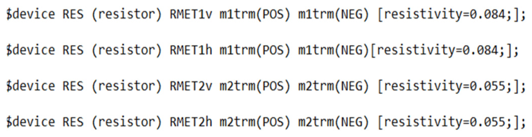
In the simplest case, the extracted parasitic resistance can be represented in PWRL as:
For the extraction of contact and via resistances, the layout is already prepared using Equation (3), and the corresponding parasitic resistances can be calculated—for example, between M3 and M2 layers, as follows:
In Equations (8) and (9), RMET2v and via2, respectively, serve as device-recognition layers for parasitic resistors.
Alternative models may also be applied, including those that consider temperature-dependent parameters, which are typically provided by semiconductor foundries.
The method for calculating parasitic gate resistance is considered next. The proposed model is based on determining the center of the transistor channel along its minimum width. In this approach, the connection to the gate is made through the channel center, and the parasitic gate resistance is proportional to half of the channel width:
Equations (10)–(13) are intended for the extraction of parasitic gate resistances, where
gate—denotes the gate region of MOS transistors;
gate_check_edge determines the gate sides according to the channel width;
gate_center places a marker (0.01 μm) at the center of the gate;
Equation (13) converts this marker into a rectangular shape of width 0.01 μm for transistors with a channel width <5 μm, effectively dividing the gate region into two equal parts with a gate_cut layer.
The $overlap_projective operation enables the efficient measurement of distances between the inner sides of edges on the first and second input layers.
After generating the gate_cut layer, the poly interconnect layer can be defined as follows:
In this context, LayPoly represents the original polysilicon layer, RESP denotes the layer defining built-in resistors, and rpcontact corresponds to the contact regions between the M1 layer and polysilicon (computed analogously to Equation (2)).
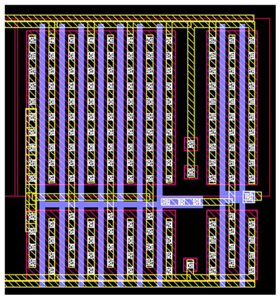
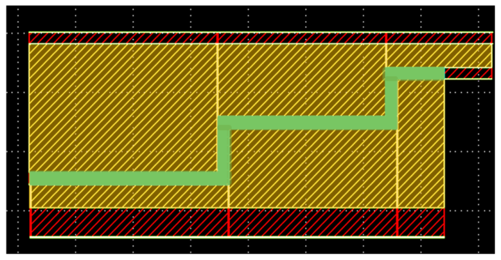
Figure 5 and
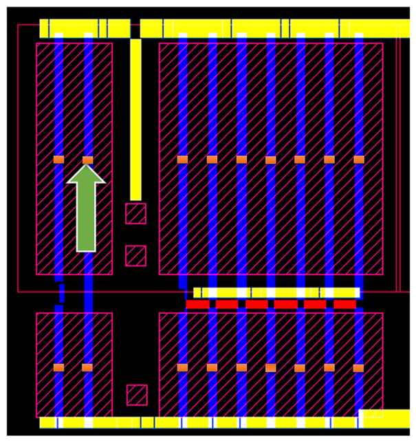
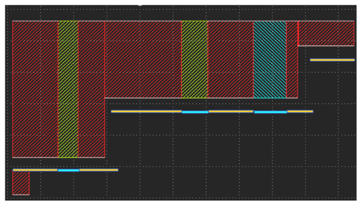
Figure 6 illustrate the buffer-cell layout and the extracted resistances, including the gate-resistance contribution.
The yellow regions in
Figure 6 indicate the parasitic resistances of M1, while the blue and red regions correspond to vertical and horizontal parasitic resistances of the polysilicon interconnects, respectively.
The green arrow marks the extracted channel center (orange rectangle) along the width direction.
To assess the influence of different types of parasitic resistance, a Register File SRAM memory instance was used. It was implemented using an 8T memory cell with 16 rows and 8-bit read/write ports for the Fab2 130 nm process node. This register file contains 5240 transistors and was chosen to minimize simulation time.
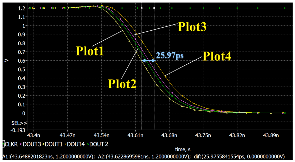
Figure 7 shows the output signal waveforms at one of the read ports of the register file for cases including different parasitic-resistance configurations:
Plot 1—simulation without parasitic resistances;
Plot 2—includes only interconnect resistances;
Plot 3—adds contact and via resistances;
Plot 4—additionally includes gate resistances.
The total delay difference between Plot 4 (all parasitic resistances included) and Plot 1 (no parasitic elements) is 25.97 ps.
In the LVS rule deck, parasitic-resistance extraction is enabled by including two optional blocks, which are activated depending on whether extraction is performed with or without parasitic elements.
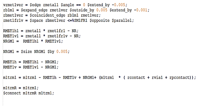
The first block is a general module responsible for generating polygons of metal and polysilicon layers used to extract their parasitic resistances, as well as polygons used for gate-resistance extraction. This block also contains the equations used for resistance calculations. An example of the rule block used to generate metal-resistance layers is shown in
Figure 8:
The second block handles connectivity through contact and via layers, where direct connections are replaced by the corresponding contact and via resistances (parasitic resistor devices). Without this modification, those resistances would be short-circuited. The corresponding rule block that replaces direct contact/via connections with parasitic resistor devices is shown in
Figure 9:
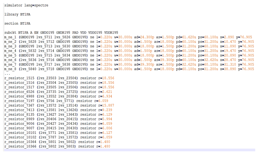
As a result, when all the above conditions are fulfilled, LVS extraction produces spicenl.lib, a netlist that is directly ready for SPICE simulation without any additional post-processing or conversion. An example of the generated SPICE-compatible spicenl.lib output is shown in
Figure 10:
4. Rule-Based Capacitance Extraction and RC-Netlist Merging
Parasitic capacitance extraction is performed separately from parasitic resistance extraction. To perform this extraction, the layout parameters used in the capacitance models must be defined [
14]. Unlike resistors, which are localized elements, parasitic capacitances are influenced by the relative positioning of routing layers at different interconnect levels. The key layout parameters required for these models include (1) the overlap area between different interconnect layers, (2) spacing between conductors within the same layer, (3) conductor width, and (4) relative alignment between interconnect layers at different levels. The overlap area between layers is a straightforward Boolean AND operation and is not discussed further.
No preliminary transformations of the layout are required for parasitic capacitance extraction, which ensures that the number of internal circuit nodes remains unchanged from the original layout.
The bus-width determination method previously applied for parasitic-resistance extraction cannot be used directly to calculate inter-wire spacing within a routing layer because the geometry and alignment of interconnects vary significantly. Therefore, a multi-step method is applied to compute distances between conductive layers, illustrated here using the M2 layer as an example.
In the first step, the edges of horizontal segments are isolated using Equation (15).
Next, polygons are formed from these edges, with their length reduced by 0.001 μm, as shown in Equation (16).
Edges of the same reduced length are then generated using Equation (17), and a polygon defining the distance to the adjacent conductor is computed using Equation (18).
The maximum inter-wire distance (%SM2FR1) at this step must be less than twice the minimum wire width plus the spacing between conductors.
Finally, we compute the edges coinciding with those derived in the previous step and extend their length by the same value used in Equation (16), thereby avoiding the creation of redundant polygons.
In the second step, the previously computed edge polygons from Equation (19) are excluded from the horizontal edges of the second metal layer using Equation (20).
The same procedure as shown in the first step is then repeated, except that the maximum allowable spacing between interconnects (%SM2FR2) is increased by the sum of the minimum wire width and the inter-wire gap.
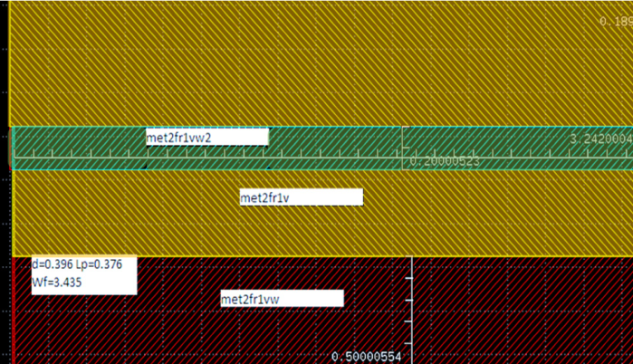
At each subsequent step, the value of the variable %SM2FRi is incremented by the sum of the minimum wire width and the inter-wire spacing until the required maximum separation distance between conductors is reached. Upon completion of this procedure, the composite polygon met2fr1v is computed as the Boolean OR sum of all polygons obtained at the preceding steps. The b2mi polygons are also important for calculating the fringe capacitance parameters, which will be discussed in the following section. To accurately determine coupling and fringe capacitances, it is essential to know the widths of the conductors within the same layer that are adjacent to the central polygon met2fr1v, as these dimensions directly affect the resulting capacitance values. A test structure illustrating this dependency is shown in
Figure 11.
Equation (25) computes the edges coinciding with the polygons met2fr1v and met2.
The $enclosure_projective operation enables measurement of the distance between the outer sides of edges in the first input layer and the inner sides of edges in the second input layer (Equation (27)).
$space_projective allows for measuring the distance between the outer edges of the input-layer boundaries.
The final Equation (28) subtracts the met2fr1vw2 layers from met2fr1vw to eliminate duplicate polygons.
Thus, the parameters Wf (width of the met2fr1v polygon), d (spacing between M2 interconnects), and Wp (average wire width) can be calculated as shown below (excluding direct capacitance computation):
Figure 12 shows the transformed layout test structure obtained by executing Equations (25)–(28).
In
Figure 13, the met2fr1v polygons are shown in yellow.
The met2fr1vw layers (light green) and met2fr1vw2 layers (red) correspond to M2 regions.
As an example, consider the M1–M2–M3 structure. The proposed method for computing layout parameters is applicable to a maximum of seven metal layers (M1–M7). The eighth metal layer is assumed to be absent, and its dielectric thickness is considered infinite.
To calculate the layout parameters for coupling and lateral capacitance models, it is necessary to define the relative positioning of interconnect layers at different routing levels. This is achieved by preparing a set of intermediate layers for the structure under consideration:
For each interconnect structure containing different conductive layers, a set of variables is defined to describe the thicknesses of the metal layers (for the central layer) and the dielectric thicknesses to the layers above and below. In the considered configuration, the M1 layer always serves as the bottom layer. For lateral capacitances, the structure can be described as follows:
The following combinations are then considered:
- -
M1M2M3 with polygon met2fr1v;
- -
M1M2M3 without polygon met2fr1v;
- -
M1M2M8 and met2fr1v without M3;
- -
M1M2M8 without met2fr1v and without M3.
The last two equations correspond to configurations in which M8 is used instead of M3.
The layer CM3M2M1v exists only in regions where met2fr1vfn is absent, that is, where no M2 layer is present within a distance smaller than the defined constraint.
Next, the layers required for coupling capacitance computation are prepared:
The final expression ensures the connectivity between the originating polygon met2fr1v and the derived polygon met2fr1v23.
For any combination of conductive layers, two types of coupling capacitances are possible: (1) symmetric capacitances, where both capacitor electrodes are identical, such as two identical M1–M2–M3 (or M1–M2–M8) electrodes with the met2fr1v polygon, and (2) asymmetric capacitances, where the electrodes differ; for example, one being M1–M2–M3 and the other M1–M2–M8. Here, the symbol “#” denotes a macro definition in PWRL. The following three #cmacro definitions describe these cases together with the #dmacro that they invoke to compute the device parameters used in the analytical coupling-capacitance models:
When the macros are expanded, the layer substitutions in the #dmacro are performed positionally—i.e., the first layer replaces the first, the second replaces the second, and so on.
The resulting symmetric and asymmetric coupling-capacitance regions are illustrated in
Figure 14.
Because test and process data provided by a semiconductor foundry generally do not include asymmetric coupling capacitances, the coupling capacitance in such cases is calculated as the average of the two corresponding symmetric capacitances.
The combined (merged) RC netlist is generated using a special run-configuration option in the LVS extraction tool.
At the initial stage, the following individual netlists are generated:
netC—the netlist containing extracted parasitic capacitances;
netR—the netlist containing extracted parasitic resistances;
netT—the reference baseline netlist without parasitic extraction (given for comparison).
The main differences between the netC and netR netlists are as follows:
Compared with the original netT, the netC has the same number of nodes since parasitic capacitance extraction does not add new nodes;
The netR, in contrast, contains significantly more nodes than the base netlist due to the addition of resistive elements;
Both netC and netR include the same active devices (MOSFETs, bipolar transistors, resistors, capacitors, etc.) as the base netlist.
In general, the numbering of active devices in netC and netR may differ because the parasitic R and C elements are attached at different stages and to different connection points in the circuit.
To establish correspondence between active devices in netC and netR, coordinate-based matching is employed.
The combined netlist (netRC) is generated as follows:
Identify transistors that share the same active device connection nodes (gates, drains, sources, etc.) and determine the number N of connections of the device terminals to each node in netC;
Determine the capacitances Cij connected between these nodes using netC. These may include both global node capacitances (to VCC, GND) and inter-node capacitances between internal nodes;
Establish the mapping between the corresponding connection nodes i and j of active elements in netC and netR;
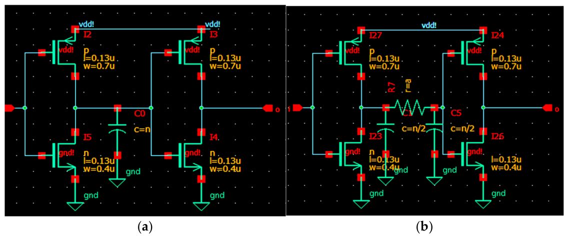
Connect the C
ij/N capacitances to the respective device terminals in netR, effectively replacing the original capacitances with π-models (as shown in
Figure 15a,b);
The internal nodes of resistors remain unchanged.
As a result, the final netRC netlist contains both active components and parasitic RC elements, providing a complete representation suitable for circuit simulation.
The accuracy of the merged netlist generated using π-models can be evaluated as follows.
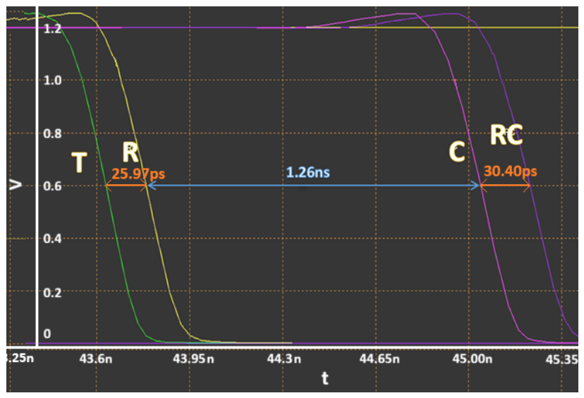
Figure 16 shows the simulated output signal delay for the test register file under the following conditions:
T—circuit without parasitic parameters;
R—circuit with only parasitic resistances;
C—circuit with only parasitic capacitances;
RC—circuit containing merged parasitic resistances and capacitances.
The accuracy of the merged netlist generated using π-models can be evaluated by comparing the incremental delay contributions of the resistive networks. The relative error introduced by the π-model replacement is defined in Equation (41).
For the test case shown in
Figure 16, Δ
TR = 25.97 ps and Δ
TRC = 30.4 ps, resulting in
≈ 17%.
In terms of global path error (estimated from the total Tacc), the difference between the two cases is calculated using Equation (42), resulting in
= 0.35%.
The resulting value is below 1% of the total access time, which is acceptable for the intended post-layout timing analysis.
5. Validation Against Foundry Reference Capacitance Data
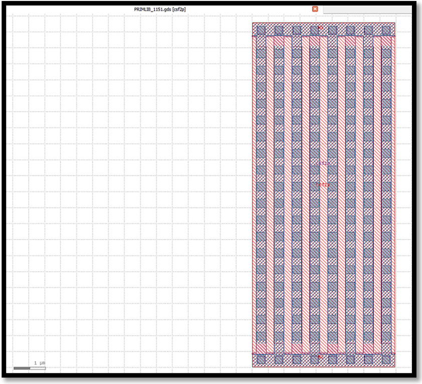
To assess extraction accuracy, the proposed flow was first evaluated using foundry-provided quality-assurance (QA) structures for a Fab1 180 nm CMOS technology. These structures represent dedicated test geometries for parasitic-capacitance extraction and correspond to reference primitive-library capacitance structures (an example is provided in
Figure 17), except that the explicit capacitance-definition layer was removed to allow parasitic extraction in the same layout region. For the evaluation, we selected the capacitor layouts csf2p, csf3p, csf4, csf5, and csf6, for which the foundry provides SPICE models with guaranteed parameters. For these capacitor layouts, extraction was performed so that the total parasitic capacitance includes the sum of the area, coupling, fringe, and via capacitances between conductive layers.
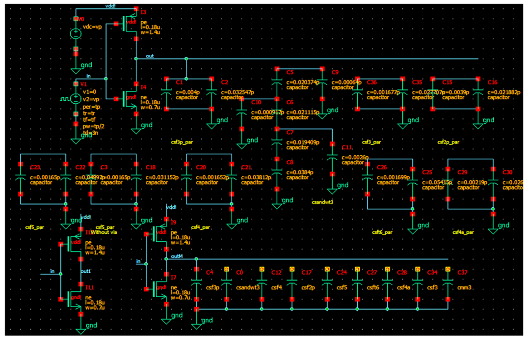
A testbench with three inverters was used. As shown in
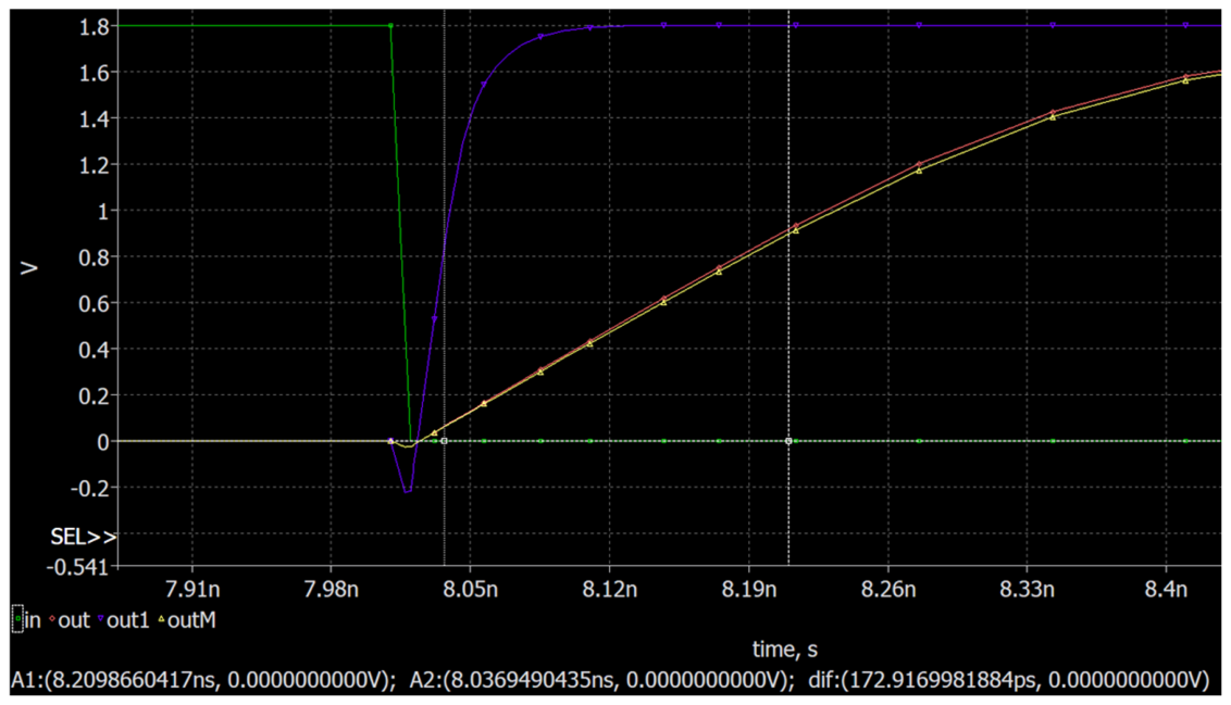
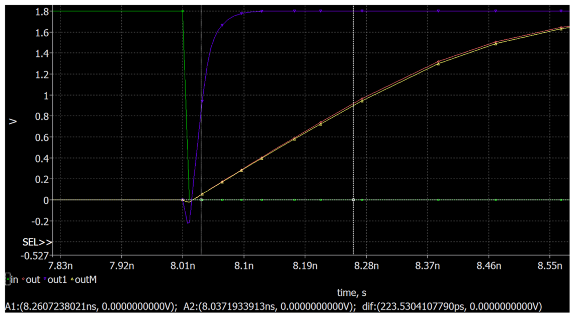
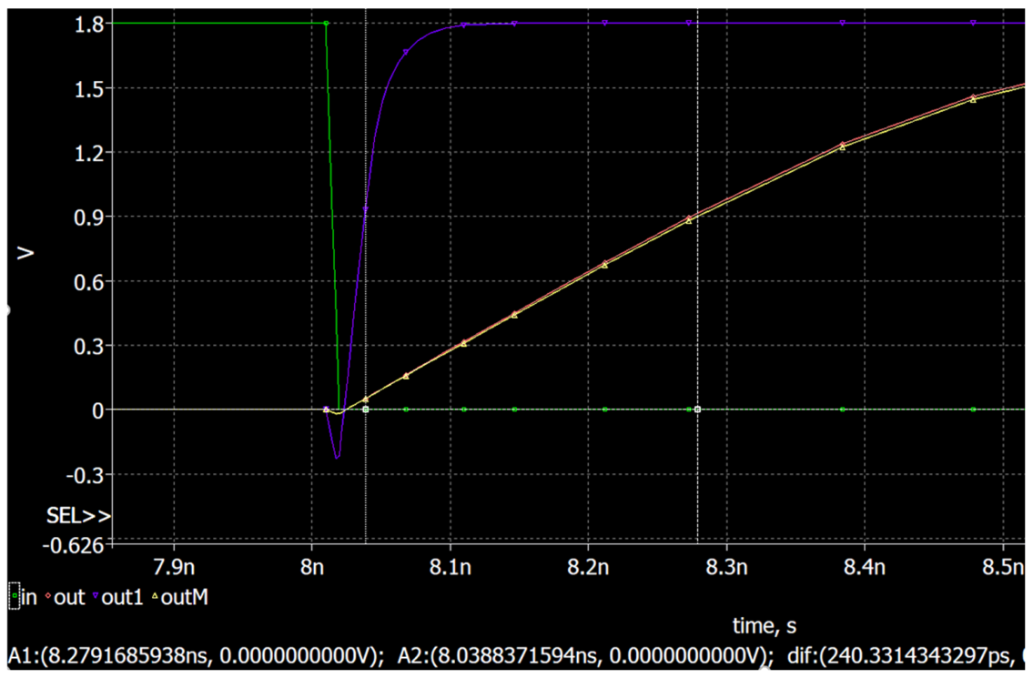
Figure 18, capacitor charging and discharging are performed by (1) the inverter composed of transistors I3 and I4 for capacitances extracted from the QA-structure layout (output Out), (2) inverter I9/I7 for capacitances described by the foundry SPICE model (output OutM), and (3) the unloaded inverter I12/I11, which accounts for intrinsic inverter capacitances in the delay calculations (output Out1).
Extraction and simulation results are shown in
Table 2 and
Table 3, respectively.
The extraction error was calculated as follows:
where
is the delay obtained using the reference model and
is the delay obtained using the extracted parasitic capacitance.
For the evaluated Fab1 180 nm QA structures, the difference between the reference-model delay and the delay obtained from the extracted parasitic capacitances was within approximately 2.8–9.4% for the analyzed structures.
This confirms that the rule-based extraction flow provides acceptable agreement with the reference capacitance models for the considered interconnect configurations.
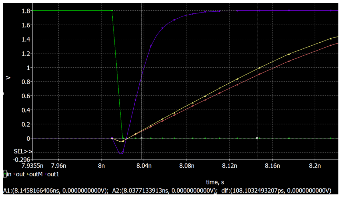
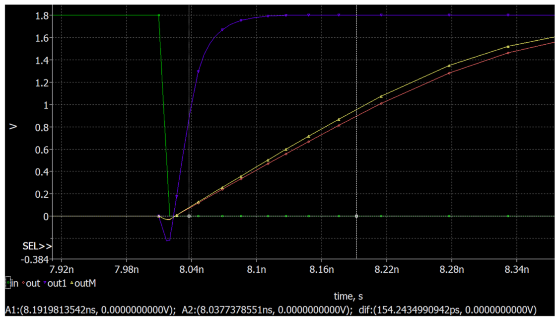
Figure 19,
Figure 20,
Figure 21,
Figure 22 and
Figure 23 provide output plots for all five capacitance models investigated. For all plots:
Out1 (violet)—no external capacitance connected (unloaded);
Out (red)—only parasitic capacitances extracted from the layout are connected;
OutM (yellow)—only the model capacitance is connected.
A second evaluation was performed using a Fab3 28 nm CMOS process and foundry-provided 2D solver reference data for representative structures such as M1OD, M1P1, and M1M2M3, where M1 denotes the first metal layer, OD denotes the active diffusion region, and P1 denotes the polysilicon layer. The comparison in
Table 4 includes bottom area capacitance Cabot, top area capacitance Catop, bottom fringe capacitance Cfbot, top fringe capacitance Cftop, and coupling capacitance Ccoup. The deviations shown in
Table 5 are generally within a few percent for area capacitances and most fringe/coupling components, while the largest deviation is observed for one fringe-capacitance component of the M1M2M3 configuration. These results indicate that the proposed analytical rule-based method can reproduce the main trends of foundry 2D reference data after technology-dependent parameter adaptation. For the M1OD and M1P1 structures, “n/a” in the tables means that the Catop and Cftop capacitances are absent because there is no layer above.
The relative extraction deviation between the rule-based result and the 2D solver reference was calculated as:
where
is the capacitance value obtained from the foundry-provided 2D solver reference data, and
is the capacitance value obtained using the proposed rule-based extraction flow. The calculated deviations are summarized in
Table 5.
6. Scaling-Aware Register-File Post-Layout Evaluation
Similarly, parasitic capacitance and resistance extraction must support the scaling of all layout parameters used in the extraction process. These include parameters such as Wf (the width of conductive polygons such as met2fr1v), d (the spacing between interconnect lines), layer intersection areas, and other geometrical descriptors.
Moreover, technological parameters such as metal layer thicknesses and dielectric layer thicknesses—which critically influence parasitic components—also exhibit process-dependent variations. Fabs typically specify these variations either in process documentation or in dedicated technology parameter files, enabling accurate modeling across multiple scaling and tolerance conditions.
To evaluate the scaling effects of parasitic parameters, a 56 × 24 register file based on an 8T static memory cell comprising 14,938 transistors was used. The circuit was developed for the Fab1 180 nm layout node with a scaling factor of S = 0.84.
Simulation was performed under the following PVT conditions: process = SS, voltage = 1 V, temperature = 27 °C.
Three simulation files were prepared:
spicenl_56 × 24_T.lib—baseline netlist;
spicenl_56 × 24_max_084.lib—netlist including parasitic capacitances with max dielectric thicknesses and min conductor thicknesses;
spicenl_56 × 24_min_084.lib—netlist including parasitic capacitances with min dielectric thicknesses and max conductor thicknesses.
A scaling factor of 0.84 was applied to both parasitic netlists. The simulation results are summarized in
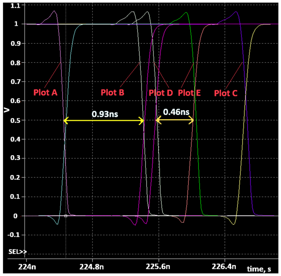
Table 6 and shown in
Figure 24, while data readout occurs on the falling edge of the clock signal. The difference in output access time Tacc between the circuits without parasitic parameters for S = 0.84 (curve A) and S = 1 (curve B) is 0.93 ns. For the configurations including parasitic parameters scaled by S = 0.84, the corresponding simulation results are shown by curves A, D, and E. The difference in output delay time Tacc between the min (D) and max (E) SPICE.lib netlists with parasitics is 0.46 ns.
The simulation results of data read operations are summarized in
Table 7 for corresponding transitions from logic high to logic low (1 → 0) and from low to high (0 → 1).
The relative error
was calculated using Equation (45):
where the indicated access-time values
Tw01
acc and
Two01
acc correspond to cases with and without the impact of parasitics, respectively, for the (0 → 1) transition.
The obtained results clearly demonstrate the significant influence of parasitic parameters on access time.
The 56 × 24 register-file instance was fabricated and functionally tested in silicon, supporting the practical feasibility of the implementation. The extraction accuracy assessment in this work is based on comparisons with foundry reference capacitance models, 2D solver data, and post-layout SPICE simulations.
7. Conclusions
The proposed rule-based RC extraction flow was evaluated using several layout-based test cases implemented in foundry-qualified LVS rule-deck environments. The method extends the standard LVS extraction flow by adding technology-dependent parasitic-resistance and parasitic-capacitance extraction sections. These sections are included as additional rule files and operate on the same connectivity and layer definitions as the foundry LVS deck. As a result, the extracted C, R, and merged RC netlists are directly suitable for SPICE simulation.
The capacitance-extraction models used in this work are based on layout-dependent parameters, including conductor widths, inter-wire spacing, overlap areas, metal thicknesses, dielectric thicknesses, and dielectric constants. The models cover area capacitances, coupling capacitances, and fringe capacitances. The resistance-extraction component includes interconnect segments, contacts, vias, and gate-resistance components.
A complementary RC-merging procedure based on π-equivalent capacitance models was introduced to combine separately extracted resistance and capacitance netlists into a compact, simulation-ready RC netlist.
An evaluation using the register-file case study showed that the π-model replacement preserves timing behavior with a global access-time error below 1%, which is acceptable for the intended post-layout timing analysis.
The register-file case studies demonstrated that parasitic resistance, parasitic capacitance, scaling factors, and process-dependent parameter variations can significantly affect access time and therefore must be considered during post-layout simulation of dense memory macros.
To adapt the method to a new technology, the technology-dependent parameters in the PWRL/LVS rule files must be updated, and the resulting extraction flow must be requalified against the target PDK reference data. This makes the approach scalable and reusable across foundry processes.
The method is intended for planar CMOS technologies and for interconnect geometries dominated by Manhattan and 45-degree routing, which are typical for digital and memory layouts. Application to FinFET, GAA, or strongly analog/RF-specific geometries requires additional investigation and technology-specific recalibration. Parasitic inductance extraction is outside the scope of this work.