Communication

Improved Properties of Post-Deposition Annealed Ga2O3/SiC and Ga2O3/Al2O3/SiC Back-Gate Transistors Fabricated by Radio Frequency Sputtering

1
Department of Electronic Materials Engineering, Kwangwoon University, Seoul 01897, Republic of Korea
2
Electronic Devices Research Team, Hyundai Motor Group, Uiwang-si 16082, Republic of Korea
3
Fraunhofer Institute for Integrated Systems and Device Technology, Schottkystrasse 10, 91058 Erlangen, Germany
*
Author to whom correspondence should be addressed.
Micro 2023, 3(4), 775-784; https://doi.org/10.3390/micro3040055
Submission received: 27 July 2023 / Revised: 31 August 2023 / Accepted: 25 September 2023 / Published: 30 September 2023

Abstract

:
The high breakdown electric field, n-type doping capability, availability of high-quality substrates, and high Baliga’s figure of merit of Ga2O3 demonstrate its potential as a next-generation power semiconductor material. However, the thermal conductivity of Ga2O3 is lower than that of other wide-bandgap materials, resulting in the degradation of the electrical performance and reduced reliability of devices. The heterostructure formation on substrates with high thermal conductivity has been noted to facilitate heat dissipation in devices. In this work, Ga2O3 thin films with an Al2O3 interlayer were deposited on SiC substrates by radio frequency sputtering. Post-deposition annealing was performed at 900 °C for 1 h to crystallize the Ga2O3 thin films. The Auger electron spectroscopy depth profiles revealed the interdiffusion of the Ga and Al atoms at the Ga2O3/Al2O3 interface after annealing. The X-ray diffraction (XRD) results displayed improved crystallinity after annealing and adding the Al2O3 interlayer. The crystallite size increased from 5.72 to 8.09 nm as calculated by the Scherrer equation using the full width at half maximum (FWHM). The carrier mobility was enhanced from 5.31 to 28.39 cm2 V−1 s−1 in the annealed Ga2O3 thin films on Al2O3/SiC. The transfer and output characteristics of the Ga2O3/SiC and Ga2O3/Al2O3/SiC back-gate transistors reflect the trend of the XRD and Hall measurement results. Therefore, this work demonstrated that the physical and electrical properties of the Ga2O3/SiC back-gate transistors can be improved by post-deposition annealing and the introduction of an Al2O3 interlayer.

1. Introduction

Although Si-based semiconductors have been widely used in power electronic devices, the narrow bandgap of Si (1.1 eV) limits its applications owing to its instability in harsh environments, such as high temperatures [1,2]. Wide-bandgap semiconductors, such as GaN, 4H-SiC, and Ga2O3, are important materials for high-frequency, -power, and -temperature devices [2,3,4]. Among these, Ga2O3 has a bandgap (~4.9 eV) that is significantly higher than that of 4H-SiC (~3.3 eV) and GaN (~3.4 eV) [5,6,7]. Owing to its high breakdown electric field (~8 MV cm−1), n-type doping capability, availability of high-quality substrates, and high Baliga’s figure of merit (~3400), Ga2O3 is attracting extensive attention as a next-generation power semiconductor material [5,6,8,9,10,11].
Despite the advantages of Ga2O3, its thermal conductivity (11–27 Wm−1 K−1) is lower than that of other wide-bandgap materials, such as SiC (370 Wm−1 K−1) and GaN (253 Wm−1 K−1). The heat generated in Ga2O3 may thus increase the lattice temperature, thereby affecting the carrier mobility in current devices, potentially resulting in critical degradation of electrical performance and device reliability [10,11]. For high-power and -frequency applications, thermal management is an inevitable consideration for reducing device degradation [11,12]. By forming heterostructures on substrates with high thermal conductivity, such as 4H-SiC, heat dissipation in devices can be facilitated [10,13].
For ε-Ga2O3 and ZnO, which have similar crystal structures, previous studies showed that an amorphous Al2O3 interface buffer layer can improve the crystallinity of the thin films [14,15]. Moreover, as Ga2O3 has an ultra-wide bandgap, few gate dielectric materials can achieve conduction band offsets of over 1 eV, which is favorable for metal-oxide-semiconductor structures [16]. Recently, materials, including Al2O3 and its alloys, are being broadly investigated for use as a gate or buffer oxide layers in metal-oxide-semiconductor field-effect transistors [16,17,18,19,20].
Channel control of MOSFETs has been improved by adopting various gate structures. Multi-gate MOSFETs (MGMOS), as well as gate-all-around (GAA) transistors, are investigated to increase the gate control and the integration density [21]. The double-gate structure consisting of top and back gate also improves the gate controllability like short channel effects [22]. However, there are not many studies on Ga2O3 transistors that investigate the effect of multi-gate including back-gate transistors. Therefore, it is necessary to study the characteristics and improve the performance of Ga2O3 transistors using back gates.
In this work, we deposited Ga2O3 and Al2O3 films on n-type 4H-SiC substrates by radio frequency (RF) sputtering. Post-deposition annealing at 900 °C was performed to crystallize the Ga2O3 thin films. The structural and electrical characteristics of the films were analyzed by Auger electron spectroscopy (AES), X-ray diffraction (XRD), Hall measurements, and current–voltage (I–V) measurements.

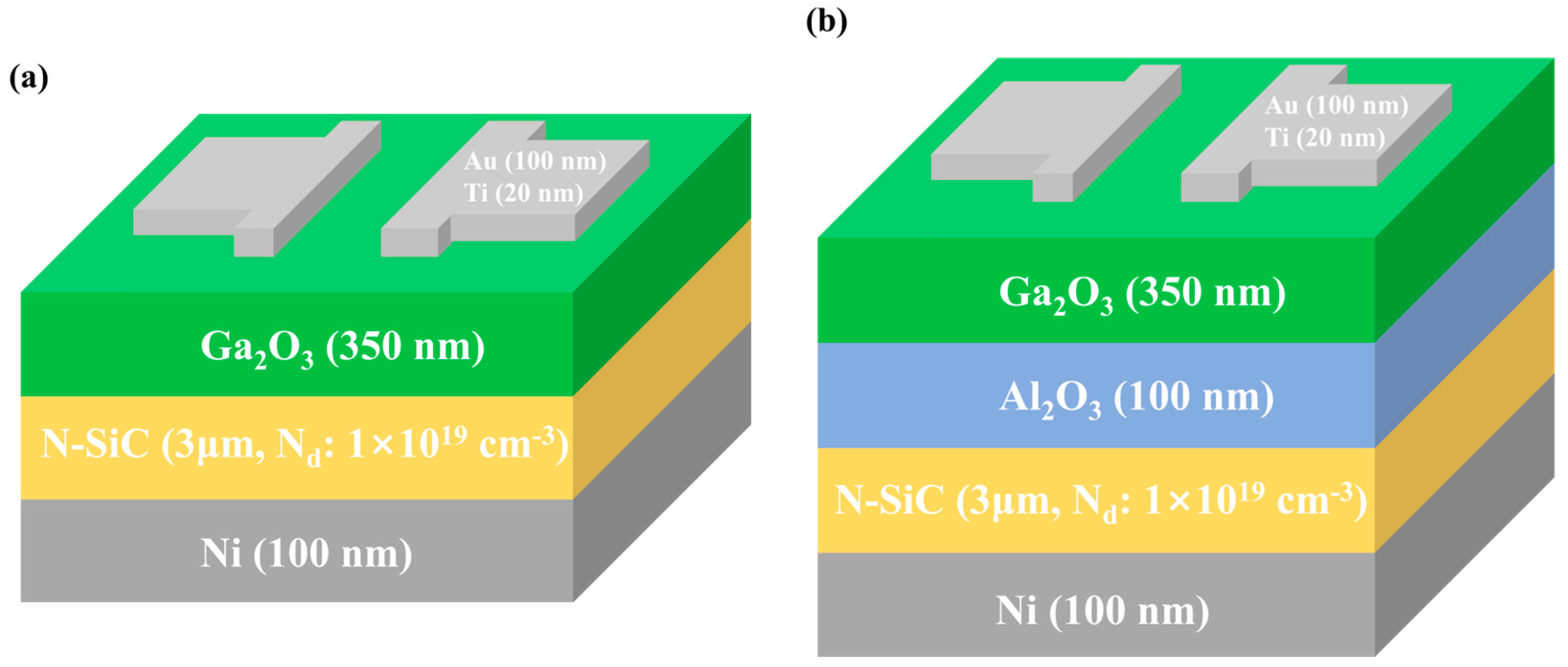
2. Experimental Details

Figure 1a,b show schematics of the fabricated structures, comprising Ga2O3 on SiC and Ga2O3 on Al2O3/SiC, respectively. N-type 4H-SiC (0004) substrates with a doping concentration of 1 × 1019 cm−3 were cleaned using acetone, methanol, and deionized water for 15 min each. The native oxide layer was stripped using a buffered oxide etch with a 30:1 ratio of HF:NH4F for 5 min. Substrate back-side metal in the form of a 100 nm thick Ni layer was deposited by an electron beam (E-beam) evaporator (KVE-T8065, Korea Vacuum Co., Ltd., Daegu, Republic of Korea) with a working pressure of 5 × 10⁻⁴ Pa. Ohmic contacts were formed at the 4H-SiC/Ni interface by rapid thermal annealing at 1000 °C for 60 s under an N2 atmosphere. Ga2O3- and Al2O3-sintered ceramic targets (Toshima Manufacturing Co., Ltd., Saitama, Japan. purity of 99.99%) were used for RF sputtering. In Figure 1a, Ga2O3 films were deposited to a thickness of ~350 nm on cleaned N-SiC substrates for 200 min. In Figure 1b, Al2O3 (~100 nm, 200 min) and Ga2O3 (~350 nm, 200 min) films were deposited on the substrates. The sputtering chamber base and working pressures were maintained at 6 × 10⁻⁴ and 3 Pa, respectively. Sputtering was performed at room temperature (25 °C), with no external substrate heating, 120 W sputtering power. and Ar gas flow rate of 4 sccm. Thin films were subsequently annealed at 900 °C for 60 min under an N2 atmosphere using a tube furnace at 101.325 × 10³ Pa. The top Ti (20 nm)/Au (100 nm) electrodes were deposited on the Ga2O3 thin films using an E-beam evaporator. The distance between the source and drain was 100 μm.

3. Characterization and Instrumentation

AES depth profiling was conducted using a PHI 710 scanning Auger probe (ULVAC-PHI, Kanagawa, Japan)with electron beam energy of 5 kV, target current of 5 nA, and a SiO2 sputtering rate of 29.4 nm·min−1 to confirm the depth-dependent atomic concentration of the samples. The crystallinity and orientations of the Ga2O3 thin films were examined using XRD (Dmax2500/PC, Rigaku, Tokyo, Japan) by 2θ scanning with CuKα radiation (λ = 0.15406 nm) at 200 mA and 40 kV. Electrical properties of the Ga2O3 thin films, including mobility, charge carrier concentrations, and resistivity, were analyzed by Hall effect measurements (HMS-5000, Ecopia Corporation, Anyang, Republic of Korea). I–V characteristics of the devices were measured by a Keithley 4200-SCS (Cleveland, OH, USA) parameter analyzer. Electrical measurements were carried out on the devices by sweeping the gate-to-source voltage (VGS) from −6 to +2 V and drain-to-source voltage (VDS) from 0 to +10 V.

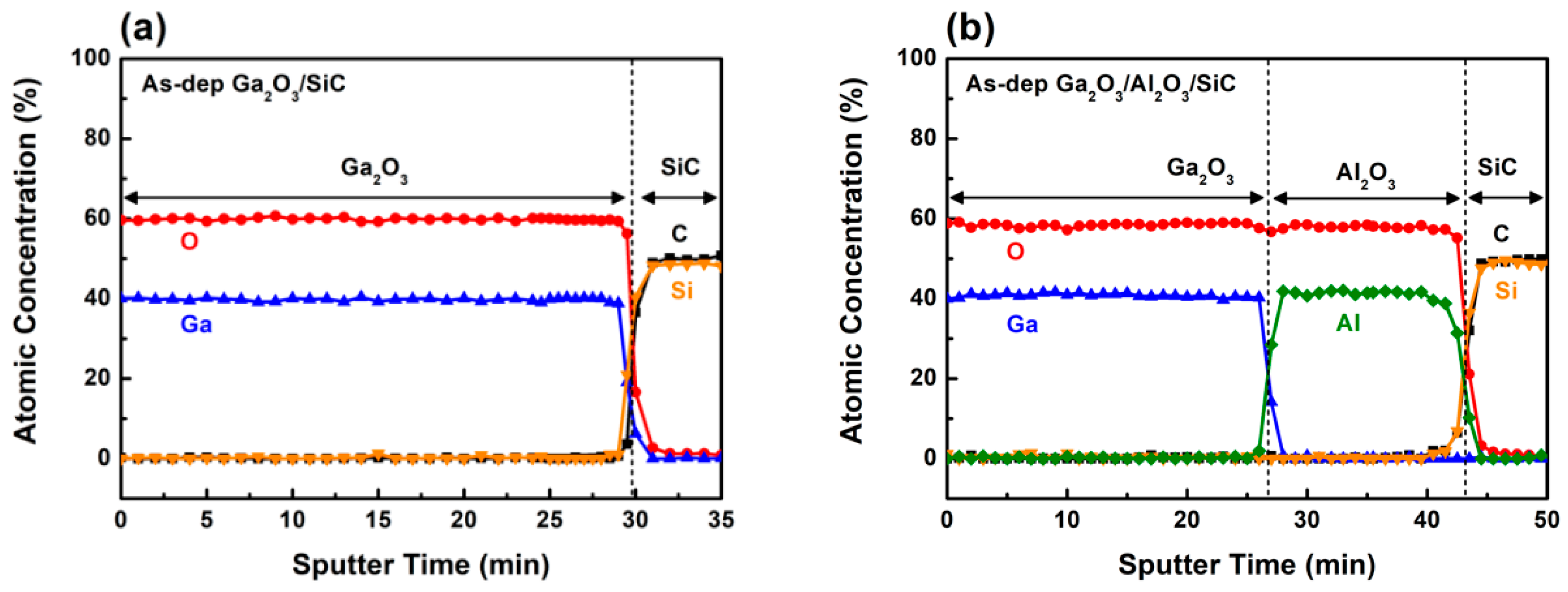
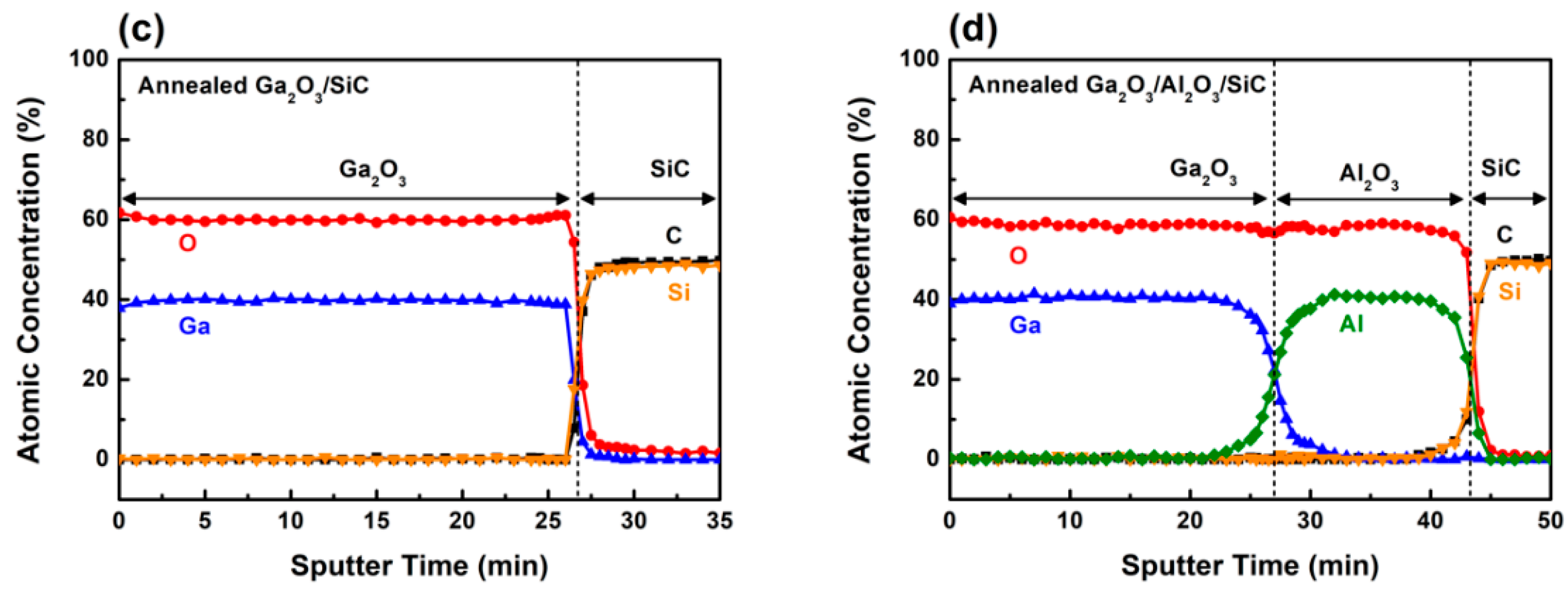
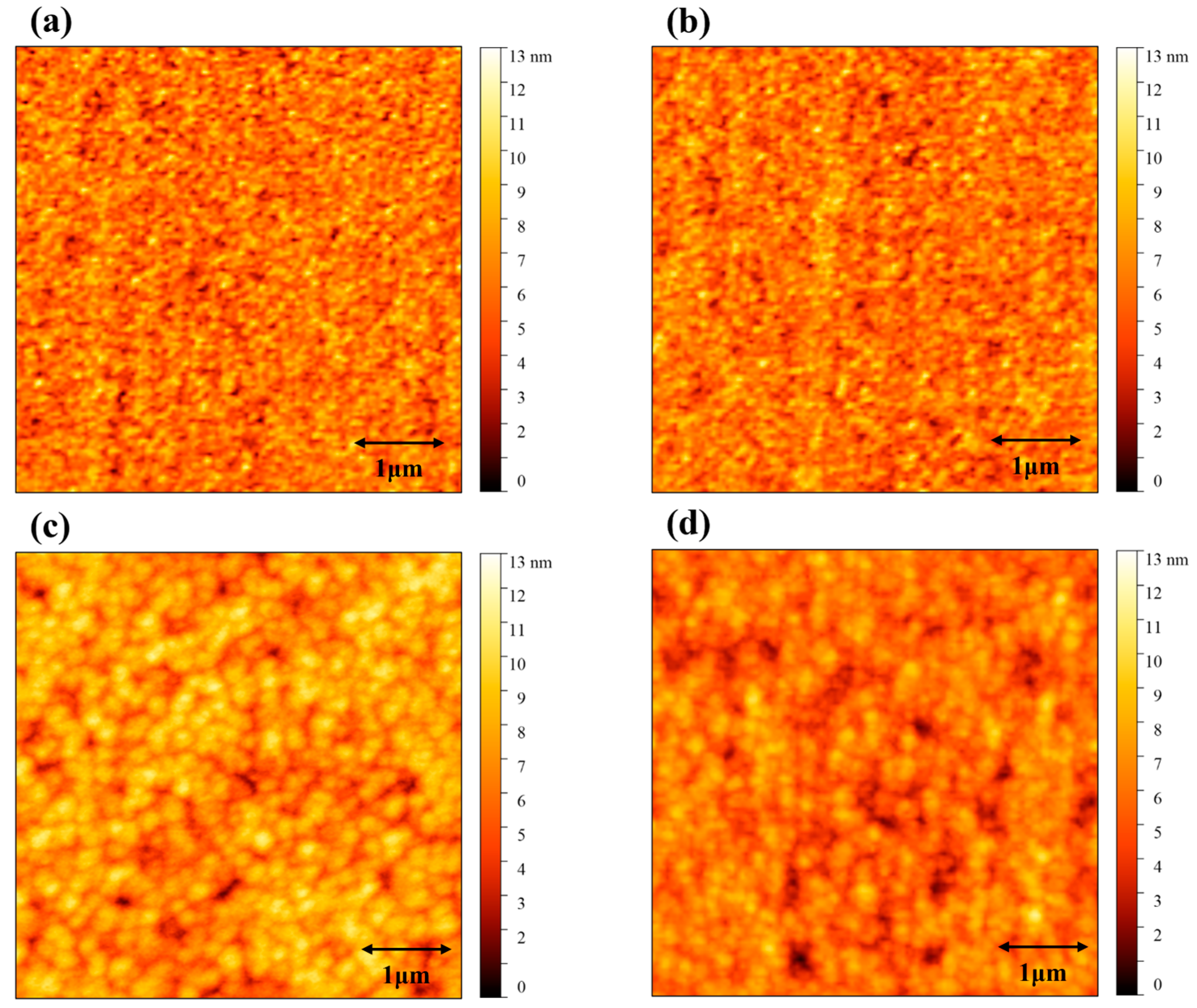
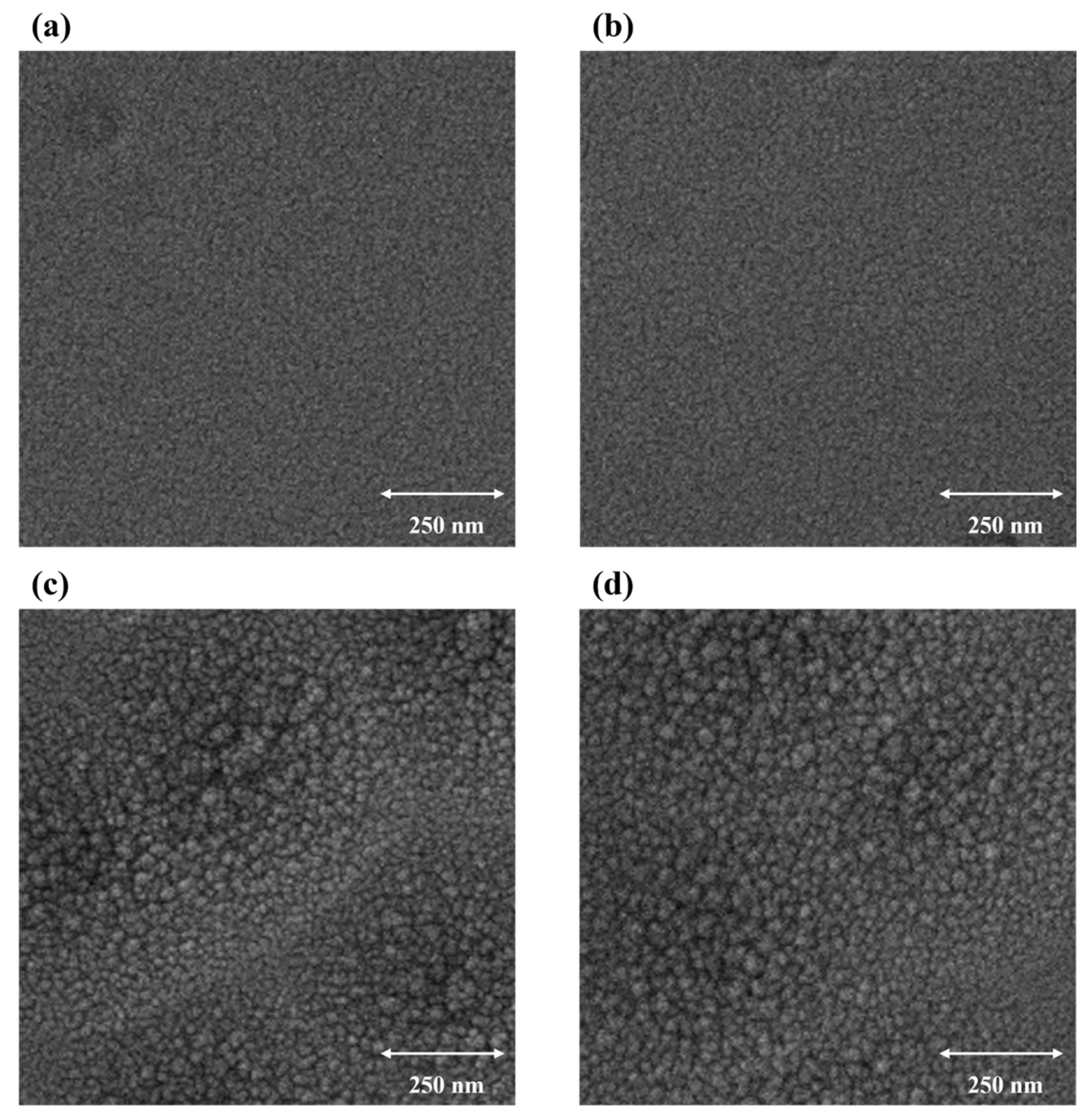
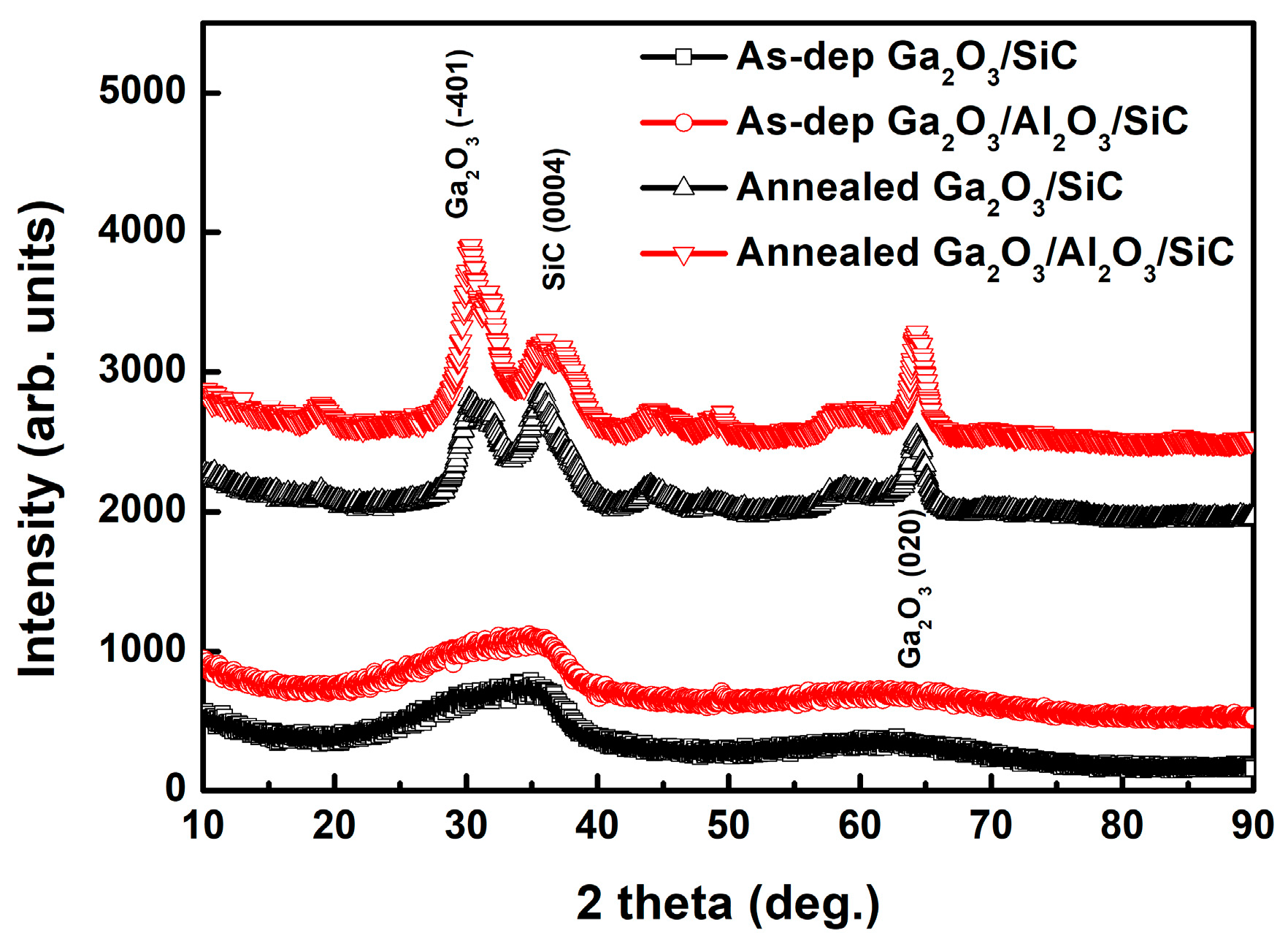
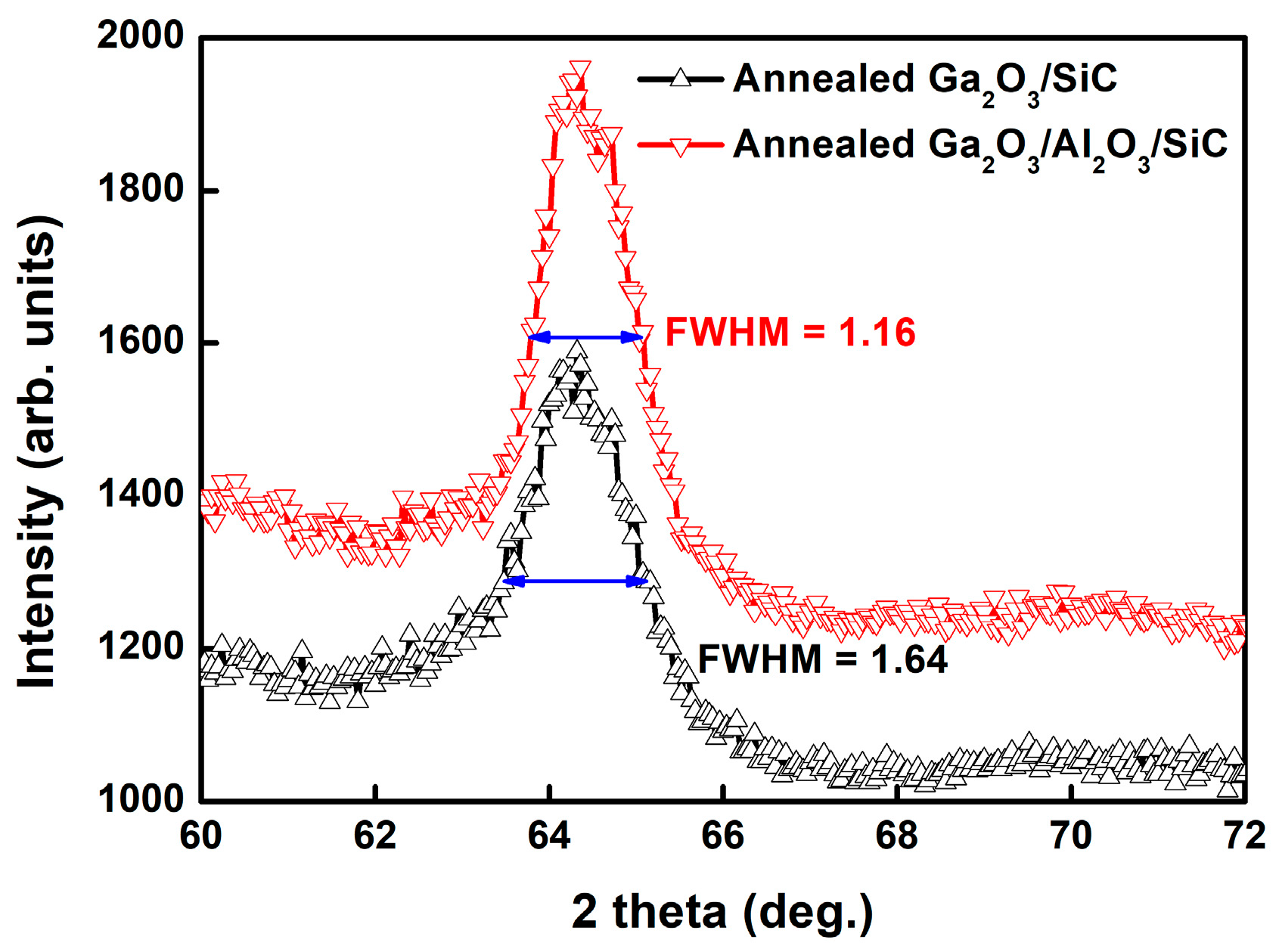
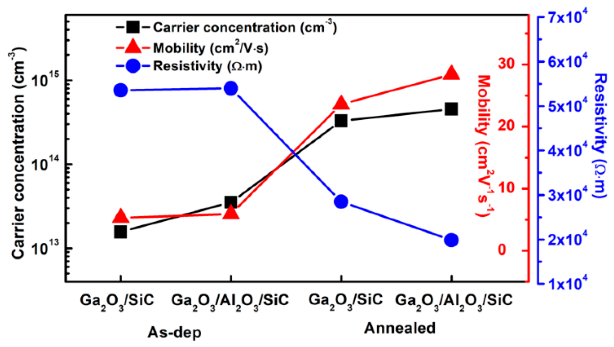
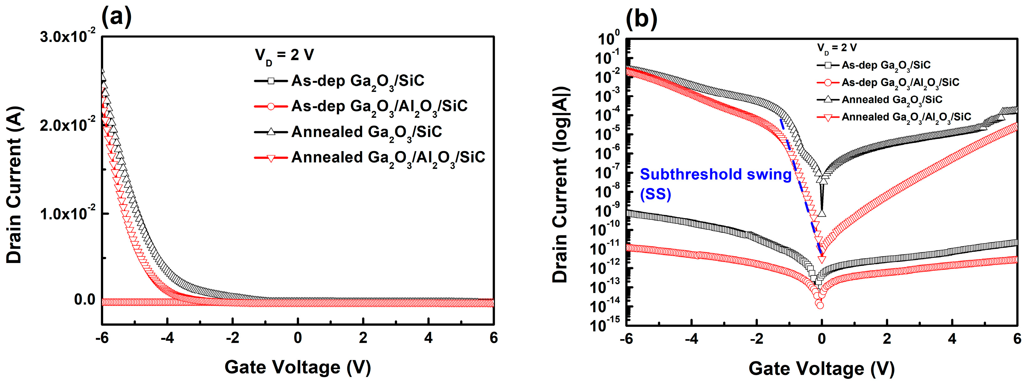
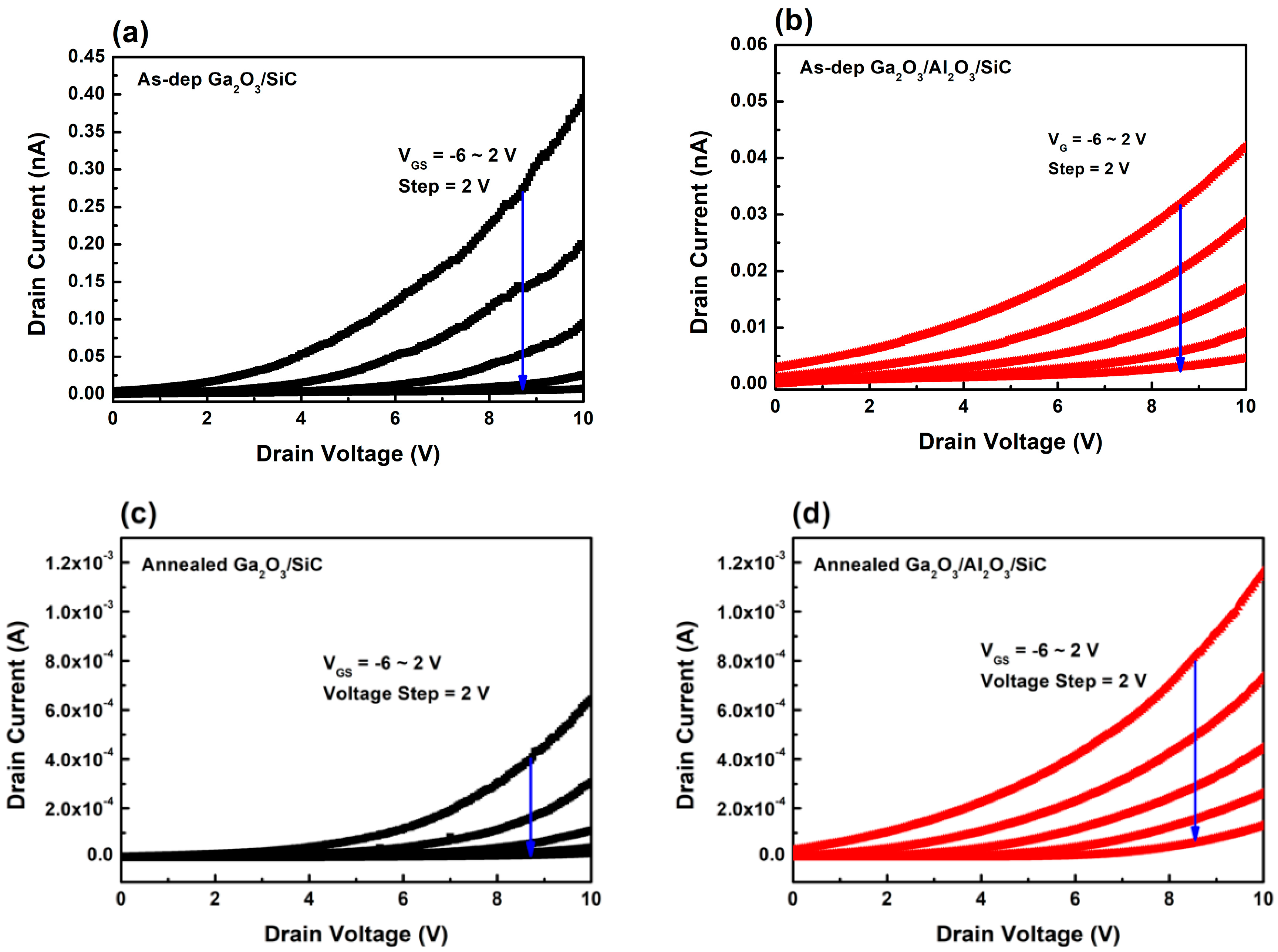
4. Results and Discussion

The AES measurements were carried out to obtain a depth profile of Ga, Al, O, Si, and C elements in order to understand their diffusion behaviors at the interface during annealing. Figure 2a–d show depth profiles of the as-deposited and annealed Ga2O3/SiC and Ga2O3/Al2O3/SiC structures. In the Ga2O3/SiC structures (Figure 2a,c), sharp interfaces were observed between the Ga2O3 thin films and SiC substrates. Meanwhile, in the Ga2O3/Al2O3/SiC structures (Figure 2b,d), Al, O, Si, and C atoms had not diffused into the opposite SiC substrates or Al2O3 films. However, gradient changes of Ga and Al atomic concentrations at the Ga2O3/Al2O3 interface indicate the interdiffusion of Ga and Al atoms [23,24]. Therefore, (AlxGa1−x)2O3 ternary compounds at the Ga2O3/Al2O3 interfaces were formed during the annealing of the devices.
In order to investigate the surface of Ga2O3 films, atomic force microscopy (AFM) was performed with a scanned area of 5 × 5 μm2. Figure 3 shows morphological AFM 2D images of as-deposited and annealed Ga2O3 films on SiC and Al2O3. The root mean square (rms) roughness was (a) 0.821, (b) 0.845, (c) 1.324, and (d) 1.359 nm, respectively. The result shows that the surfaces of the annealed samples are rougher than the as deposited sample, and thus the annealing treatment may provide energy to atoms in the films and induce the recrystallization of Ga2O3 films.
Figure 4 illustrates the scanning electron microscopy (SEM) images of as deposited and annealed Ga2O3 films on SiC and Al2O3, respectively. It can be clearly seen that larger crystals were formed after the annealing process at 900 °C. Moreover, as shown in Figure 4c,d, annealed Ga2O3 thin films possess well-defined grain boundaries which may affect the Hall mobility of devices.
The XRD 2θ–θ patterns at θ of 10–90° of the RF-sputtered Ga2O3 thin films with and without an Al2O3 interlayer are shown in Figure 5. For the as-deposited samples, only strong diffraction peaks of the 4H-SiC (0004) substrates were noted [25,26]. The absence of any Ga2O3 peaks indicates that the as-deposited thin films are in an amorphous state [27]. After annealing at 900 °C, three main peaks were noted at 30.36°, 64.36°, and 35.48°, corresponding to Ga2O3(–401) [28], Ga2O3(020) [9,29], and 4H-SiC(0004), respectively. Furthermore, diffraction peaks of Al2O3 were not observed in the Ga2O3/Al2O3/SiC structure, indicating that the deposited Al2O3 films remained amorphous, even after annealing at 900 °C. This can be attributed to the low annealing temperature in this experiment, which, according to the literature, is too low to cause a phase change from amorphous to crystalline Al2O3 [30]. The presence of the lattice mismatch buffering Al2O3 interlayer, along with any (AlxGa1−x)2O3 formed at the Ga2O3/Al2O3 interface, resulted in enhanced diffraction peak intensities from the (–401) and (020) Ga2O3 crystal faces [14,15,31,32], which may connect to increased crystallite size.
The full width at half maximum (FWHM) and crystallite sizes were extracted from the (020) peaks to compare the effects of the Al2O3 interlayer on the crystallinity of the annealed Ga2O3 thin films. Figure 6 shows XRD patterns of the (020) peaks and FWHM values of the annealed Ga2O3 thin films. The Scherrer equation (Equation (1)) was used to calculate the crystallite sizes:
F W H M = K λ L cos θ
where K is the shape factor (0.9), L is the crystallite sizes, θ is the Bragg diffraction angle [2], and λ is the wavelength of the CuKα X-ray source (0.15406 nm). The crystallite size of the Ga2O3 thin films tends to increase from 5.72 to 8.09 nm with the addition of the Al2O3 interlayer. The crystallite size is inversely proportional to the number of grain boundaries, which are a major factor in carrier mobility degradation [33]. This suggests that the samples with the Al2O3 interlayer may exhibit improved electrical characteristics.
Hall measurements of the Ga2O3 thin films were performed (at room temperature) to examine the influence of annealing and the presence or absence of an Al2O3 interlayer on the electrical properties of the sample devices. Figure 7 shows the carrier concentration, mobility, and resistivity of the different Ga2O3 thin films, according to whether they had been annealed after deposition or not, and relating to the device structure, with or without an Al2O3 interlayer. After annealing of the thin films, the Hall mobility increased, indicating the effect of Ga2O3 crystallization on the Hall mobility. The annealed Ga2O3/Al2O3/SiC devices exhibited the highest charge carrier concentration and mobility (4.52 × 1014 cm−3 and 25.65 cm2 V−1 s−1, respectively) and lowest resistivity (19.86 × 10³ Ωm). As previously hypothesized, the improved Hall mobility can be attributed to the larger crystallite size due to the reduction in grain boundary scattering [34,35,36].
The back-gate transistors, as shown in Figure 1a,b, have a source–drain spacing of 100 μm with highly doped SiC/Ni back gates. Figure 8a,b show the electrical transfer characteristics of the as-deposited and annealed Ga2O3/SiC and Ga2O3/Al2O3/SiC back-gate transistors. The subthreshold swing (SS), defined by the VGS variations required for the ten-fold increase in IDS, is given by the maximum slope in the transfer curve in a logarithmic scale [37] and can be extracted by (Equation (2)):
S S = d V G S d log I D S
The on and off currents, on/off ratio (VGS = ±6 V), and SS of the devices are shown in Table 1. The annealed Ga2O3/Al2O3/SiC transistors have the highest on/off ratio of 8.27 × 10² and the lowest SS of 154 mV·dec−1.
The IDS-VDS output curves were measured by sweeping the VDS from 0 to +10 V, whereas VGS was biased from −6 to +2 V. Figure 9a–d show the electrical output characteristics of the back-gate transistors. The transistors with the as-deposited Ga2O3 films exhibited a maximum IDS below 10−9 A, whereas the transistors with annealed Ga2O3 films featured currents over 10−4 A. Annealed samples with an Al2O3 layer exhibited the highest carrier mobility, resulting in the highest on-current level. This result is mainly attributed to the improved crystallinity of the Ga2O3 films by annealing [38] and the addition of the Al2O3 interlayer [14,15,31,32]. The larger crystallite grains, and thus enhanced crystallinity, apparently mitigate the parasitic resistance [39] and grain boundary scattering of thin films [33,36] of the Ga2O3 thin films, resulting in improved device performance.

5. Conclusions

In this study, Ga2O3 and Al2O3 thin films were deposited on 4H-SiC substrates using RF sputtering to compare the effects of an Al2O3 interlayer on the morphological and electrical properties of the manufactured thin films and resulting devices. Through AES depth profiling, we confirmed that Al and Ga atoms interdiffusion at the Ga2O3/Al2O3 interface during annealing at 900 °C. XRD results brought to light an improved crystallinity of the Ga2O3 thin films after annealing and adding the Al2O3 layer. Annealed Ga2O3 film on Al2O3/SiC displayed the highest carrier concentration and mobility of 4.52 × 1014 cm−3 and 25.65 cm2 V−1 s−1, respectively, as well as the lowest resistivity of 19.86 × 10³ Ω·m. These enhanced electrical properties of the annealed Ga2O3 on Al2O3/SiC affected the transfer and output characteristics, resulting in the highest on/off ratio (8.27 × 10²) and lowest SS (154 mV·dec−1). Thus, introducing an Al2O3 interlayer in RF-sputtered Ga2O3/SiC back-gate transistors improved the electrical characteristics of the devices.

Author Contributions

Conceptualization, H.-J.L. and S.-M.K.; Data curation, H.-J.L. and D.H.C.; Formal analysis, H.-J.L. and D.-W.B.; Funding acquisition, S.-M.K.; Investigation, H.-J.L., M.L., and S.-M.K.; Methodology, H.-J.L. and S.-H.C.; Project administration, S.-M.K.; Software, H.-J.L., G.-H.L. and N.Y.J.; Supervision, S.-M.K.; Validation, H.-J.L., T.E., and S.-M.K.; Writing—original draft, H.-J.L.; Writing—review and editing, M.A.S. and S.-M.K. All authors have read and agreed to the published version of the manuscript.

Funding

This work was supported by the Kwangwoon University in 2023, the Korea Institute of Energy Technology Evaluation and Planning (KETEP) (20214000000700) and the Korea Evaluation Institute of Industrial Technology (KEIT) (20016102) grant funded by the MOTIE of Korea.

Data Availability Statement

Data supporting the published results can be obtained from the authors upon reasonable request.

Acknowledgments

Hee-Jae Lee and Sang-Mo Koo thank Tobias Erlbacher, Minwho Lim, and the Fraunhofer Institute for Integrated Systems and Devices Technology (IISB) for allowing the research–visit collaboration of the graduate students.

Conflicts of Interest

The authors declare no conflict of interest.

References

  1. Oh, S.; Yang, G.; Kim, J. Electrical characteristics of vertical Ni/β-Ga2O3 Schottky barrier diodes at high temperatures. ECS J. Solid State Sci. Technol. 2016, 6, Q3022. [Google Scholar] [CrossRef]
  2. Byun, D.W.; Lee, Y.J.; Oh, J.M.; Schweitz, M.A.; Koo, S.M. Morphological and electrical properties of β-Ga2O3/4H-SiC heterojunction diodes. Electron. Mater. Lett. 2021, 17, 479–484. [Google Scholar] [CrossRef]
  3. Pérez-Tomás, A.; Jennings, M.R.; Davis, M.; Shah, V.; Grasby, T.; Covington, J.A.; Mawby, P.A. High doped MBE Si p–n and n–n heterojunction diodes on 4H-SiC. Microelectron. J. 2007, 38, 1233–1237. [Google Scholar] [CrossRef]
  4. Oshima, T.; Kaminaga, K.; Mukai, A.; Sasaki, K.; Masui, T.; Kuramata, A.; Yamakoshi, S.; Fujita, S.; Ohtomo, A. Formation of semi-insulating layers on semiconducting β-Ga2O3 single crystals by thermal oxidation. Jpn. J. Appl. Phys. 2013, 52, 051101. [Google Scholar] [CrossRef]
  5. Lee, H.J.; Shin, M.C.; Moon, S.Y.; Byun, D.W.; Kim, M.Y.; Lee, H.J.; Lee, G.H.; Jung, S.W.; Schweitz, M.A.; Park, J.; et al. Bandgap modulation and electrical characteristics of (AlxGa1−x)2O3/4H-SiC thin film heterostructures. Thin Solid Film. 2022, 754, 139276. [Google Scholar] [CrossRef]
  6. Wang, Y.; Xu, W.; You, T.; Mu, F.; Hu, H.; Liu, Y.; Huang, H.; Suga, T.; Han, G.; Ou, X.; et al. β-Ga2O3 MOSFETs on the Si substrate fabricated by the ion-cutting process. Sci. China Phys. Mech. Astron. 2020, 63, 277311. [Google Scholar] [CrossRef]
  7. Zhang, J.; Shi, J.; Qi, D.C.; Chen, L.; Zhang, K.H. Recent progress on the electronic structure, defect, and doping properties of Ga2O3. APL Mater. 2020, 8, 020906. [Google Scholar] [CrossRef]
  8. Lee, Y.J.; Schweitz, M.A.; Oh, J.M.; Koo, S.M. Influence of annealing atmosphere on the characteristics of Ga2O3/4H-SiC n-n heterojunction diodes. Materials 2020, 13, 434. [Google Scholar] [CrossRef]
  9. Bhuiyan, A.F.M.; Feng, Z.; Johnson, J.M.; Huang, H.L.; Sarker, J.; Zhu, M.; Karim, M.R.; Mazumder, B.; Hwang, J.; Zhao, H. Phase transformation in MOCVD growth of (AlxGa1−x)2O3 thin films. APL Mater. 2020, 8, 031104. [Google Scholar] [CrossRef]
  10. Vaca, D.; Yates, L.; Nepal, N.; Katzer, D.S.; Downey, B.P.; Wheeler, V.; Meyer, D.J.; Graham, S.; Kumar, S. Thermal conductivity of β-Ga2O3 thin films grown by molecular beam epitaxy. In Proceedings of the 2020 19th IEEE Intersociety Conference on Thermal and Thermomechanical Phenomena in Electronic Systems (ITherm), Orlando, FL, USA, 21–23 July 2020; pp. 1011–1016. [Google Scholar]
  11. Santia, M.D.; Tandon, N.; Albrecht, J.D. Lattice thermal conductivity in β-Ga2O3 from first principles. Appl. Phys. Lett. 2015, 107, 041907. [Google Scholar] [CrossRef]
  12. Cheng, Z.; Yates, L.; Shi, J.; Tadjer, M.J.; Hobart, K.D.; Graham, S. Thermal conductance across β-Ga2O3-diamond van der Waals heterogeneous interfaces. APL Mater. 2019, 7, 031118. [Google Scholar] [CrossRef]
  13. Bar-Cohen, A.; Albrecht, J.D.; Maurer, J.J. Near-junction thermal management for wide bandgap devices. In Proceedings of the 2011 IEEE Compound Semiconductor Integrated Circuit Symposium (CSICS), Waikoloa, HI, USA, 16–19 October 2011; pp. 1–5. [Google Scholar]
  14. Wang, T.; Wu, H.; Chen, C.; Liu, C. Growth, optical, and electrical properties of nonpolar m-plane ZnO on p-Si substrates with Al2O3 buffer layers. Appl. Phys. Lett. 2012, 100, 011901. [Google Scholar] [CrossRef]
  15. Qian, H.; Zhang, X.; Ma, Y.; Zhang, L.; Chen, T.; Wei, X.; Tang, W.; Zhou, X.; Feng, B.; Fan, Y.; et al. Quasi-vertical ε-Ga2O3 solar-blind photodetectors grown on p-Si substrates with Al2O3 buffer layer by metalorganic chemical vapor deposition. Vacuum 2022, 200, 111019. [Google Scholar] [CrossRef]
  16. Jian, Z.; Sayed, I.; Liu, W.; Mohanty, S.; Ahmadi, E. Characterization of MOCVD-grown AlSiO gate dielectric on β-Ga2O3 (001). Appl. Phys. Lett. 2021, 118, 172102. [Google Scholar] [CrossRef]
  17. Wang, T.; Li, W.; Ni, C.; Janotti, A. Band gap and band offset of Ga2O3 and (AlxGa1−x)2O3 alloys. Phys. Rev. Appl. 2018, 10, 011003. [Google Scholar] [CrossRef]
  18. Feng, Z.; Feng, Q.; Zhang, J.; Zhang, C.; Zhou, H.; Li, X.; Huang, L.; Xu, L.; Hu, Y.; Zhao, S.; et al. Band alignments of SiO2 and HfO2 dielectrics with (AlxGa1−x)2O3 film (0 ≤ x ≤ 0.53) grown on Ga2O3 buffer layer on sapphire. J. Alloys Compd. 2018, 745, 292–298. [Google Scholar] [CrossRef]
  19. Bhuiyan, A.F.M.; Feng, Z.; Johnson, J.M.; Huang, H.L.; Hwang, J.; Zhao, H. Band offsets of (100) β-(AlxGa1−x)2O3/β-Ga2O3 heterointerfaces grown via MOCVD. Appl. Phys. Lett. 2020, 117, 252105. [Google Scholar] [CrossRef]
  20. Singh, P.; Jha, R.K.; Singh, R.K.; Singh, B.R. Preparation and characterization of Al2O3 film deposited by RF sputtering and plasma enhanced atomic layer deposition. J. Vac. Sci. Technol. B Nanotechnol. Microelectron. Mater. Process. Meas. Phenom. 2018, 36, 04G101. [Google Scholar] [CrossRef]
  21. Herrera, F.Á.; Hirano, Y.; Miura-Mattausch, M.; Iizuka, T.; Kikuchihara, H.; Mattausch, H.J.; Ito, A. Advanced short-channel-effect modeling with applicability to device optimization—Potentials and scaling. IEEE Trans. Electron Devices 2019, 66, 3726–3733. [Google Scholar] [CrossRef]
  22. Madadi, D.; Orouji, A.A. β-Ga2O3 double gate junctionless FET with an efficient volume depletion region. Phys. Lett. A 2021, 412, 127575. [Google Scholar] [CrossRef]
  23. Li, Z.; Wu, Y.; Feng, B.; Li, Y.; Liu, T.; Feng, J.; Chen, X.; Huang, R.; Xu, L.; Li, Z.; et al. Bandgap Tailoring of Monoclinic Single-Phase β-(AlxGa1−x)2O3 (0 ≤ x ≤ 0.65) Thin Film by Annealing β-Ga2O3/Al2O3 Heterojunction at High Temperatures. Phys. Status Solidi A 2021, 218, 2000785. [Google Scholar] [CrossRef]
  24. Liao, C.H.; Li, K.H.; Torres-Castanedo, C.G.; Zhang, G.; Li, X. Wide range tunable bandgap and composition β-phase (AlGa)2O3 thin film by thermal annealing. Appl. Phys. Lett. 2021, 118, 032103. [Google Scholar] [CrossRef]
  25. Nakagomi, S.; Sakai, T.; Kikuchi, K.; Kokubun, Y. β-Ga2O3/p-type 4H-SiC heterojunction diodes and applications to deep-UV photodiodes. Phys. Status Solidi A 2019, 216, 1700796. [Google Scholar] [CrossRef]
  26. Nepal, N.; Katzer, D.S.; Downey, B.P.; Wheeler, V.D.; Nyakiti, L.O.; Storm, D.F.; Hardy, M.T.; Freitas, J.A.; Jin, E.N.; Vaca, D.; et al. Heteroepitaxial growth of β-Ga2O3 films on SiC via molecular beam epitaxy. J. Vac. Sci. Technol. A Vac. Surf. Film. 2020, 38, 063406. [Google Scholar] [CrossRef]
  27. Singh, A.K.; Gupta, M.; Sathe, V.; Katharria, Y.S. Effect of annealing temperature on β-Ga2O3 thin films deposited by RF sputtering method. Superlattices Microstruct. 2021, 156, 106976. [Google Scholar] [CrossRef]
  28. Yu, J.; Nie, Z.; Dong, L.; Yuan, L.; Li, D.; Huang, Y.; Zhang, L.; Zhang, Y.; Jia, R. Influence of annealing temperature on structure and photoelectrical performance of β-Ga2O3/4H-SiC heterojunction photodetectors. J. Alloys Compd. 2019, 798, 458–466. [Google Scholar] [CrossRef]
  29. Anhar Uddin Bhuiyan, A.F.M.; Feng, Z.; Johnson, J.M.; Chen, Z.; Huang, H.L.; Hwang, J.; Zhao, H. MOCVD epitaxy of β-(AlxGa1−x)2O3 thin films on (010) Ga2O3 substrates and N-type doping. Appl. Phys. Lett. 2019, 115, 120602. [Google Scholar] [CrossRef]
  30. Zhang, L.; Jiang, H.C.; Liu, C.; Dong, J.W.; Chow, P. Annealing of Al2O3 thin films prepared by atomic layer deposition. J. Phys. D Appl. Phys. 2007, 40, 3707. [Google Scholar] [CrossRef]
  31. Kim, B.; Yang, D.; Sohn, W.; Lee, S.; Jang, T.; Yoon, E.; Park, Y.; Jang, H.W. Strain relaxation and dislocation annihilation in compositionally graded α-(AlxGa1−x)2O3 layer for high voltage α-Ga2O3 power devices. Acta Mater. 2021, 221, 117423. [Google Scholar] [CrossRef]
  32. Cheng, Y.; Zhang, C.; Xu, Y.; Li, Z.; Chen, D.; Zhu, W.; Feng, Q.; Xu, S.; Zhang, J.; Hao, Y. Heteroepitaxial growth of β-Ga2O3 thin films on c-plane sapphire substrates with β-(AlxGa1−x)2O3 intermediate buffer layer by mist-CVD method. Mater. Today Commun. 2021, 29, 102766. [Google Scholar] [CrossRef]
  33. Bhuvana, K.P.; Elanchezhiyan, J.; Gopalakrishnan, N.; Balasubramanian, T. Influence of grain size on the properties of AlN doped ZnO thin film. Mater. Sci. Semicond. Process. 2011, 14, 84–88. [Google Scholar] [CrossRef]
  34. Assunção, V.; Fortunato, E.; Marques, A.; Gonçalves, A.; Ferreira, I.; Águas, H.; Martins, R. New challenges on gallium-doped zinc oxide films prepared by rf magnetron sputtering. Thin Solid Film. 2003, 442, 102–106. [Google Scholar] [CrossRef]
  35. Wang, D.; Ma, X.; Xiao, H.; Le, Y.; Ma, J. Ta-doped epitaxial β-Ga2O3 films deposited on SrTiO3 (100) substrates by MOCVD. Mater. Sci. Semicond. Process. 2021, 128, 105749. [Google Scholar] [CrossRef]
  36. Wang, S.; Hui, S.; Peng, K.; Bailey, T.P.; Zhou, X.; Tang, X.; Uher, C. Grain boundary scattering effects on mobilities in p-type polycrystalline SnSe. J. Mater. Chem. C 2017, 5, 10191–10200. [Google Scholar] [CrossRef]
  37. Oh, B.Y.; Jeong, M.C.; Ham, M.H.; Myoung, J.M. Effects of the channel thickness on the structural and electrical characteristics of room-temperature fabricated ZnO thin-film transistors. Semicond. Sci. Technol. 2007, 22, 608. [Google Scholar] [CrossRef]
  38. Makeswaran, N.; Battu, A.K.; Deemer, E.; Ramana, C.V. Crystal growth and structure–property optimization of thermally annealed nanocrystalline Ga2O3 films. Cryst. Growth Des. 2020, 20, 2893–2903. [Google Scholar] [CrossRef]
  39. Patel, S.L.; Chander, S.; Purohit, A.; Kannan, M.D.; Dhaka, M.S. Influence of NH4Cl treatment on physical properties of CdTe thin films for absorber layer applications. J. Phys. Chem. Solids 2018, 123, 216–222. [Google Scholar] [CrossRef]
Figure 1. Schematic of the (a) Ga2O3/SiC and (b) Ga2O3/Al2O3/SiC structures.
Micro 03 00055 g001
Figure 2. AES depth profiles of the as-deposited and annealed (900 °C) (a,c) Ga2O3/SiC and (b,d) Ga2O3/Al2O3/SiC structures, respectively.
Micro 03 00055 g002aMicro 03 00055 g002b
Figure 3. AFM images of the as-deposited and annealed (a,c) Ga2O3/SiC and (b,d) Ga2O3/Al2O3/SiC back-gate transistors, respectively.
Micro 03 00055 g003
Figure 4. SEM images of the as-deposited and annealed (a,c) Ga2O3/SiC and (b,d) Ga2O3/Al2O3/SiC back-gate transistors, respectively.
Micro 03 00055 g004
Figure 5. XRD 2θ—θ wide-scan spectra of the Ga2O3 thin films.
Micro 03 00055 g005
Figure 6. XRD patterns of (020) peaks and the extracted FWHM values of annealed Ga2O3 thin films, with or without an Al2O3 interlayer.
Micro 03 00055 g006
Figure 7. Hall mobility, carrier concentration, and resistivity of the Ga2O3 thin films.
Micro 03 00055 g007
Figure 8. Transfer characteristics of the as-deposited and annealed Ga2O3/SiC and Ga2O3/Al2O3/SiC back-gate transistors in (a) linear and (b) logarithmic scales.
Micro 03 00055 g008
Figure 9. Output characteristics of the as-deposited and annealed (a,c) Ga2O3/SiC and (b,d) Ga2O3/Al2O3/SiC back-gate transistors, respectively.
Micro 03 00055 g009
Table 1. Electrical characteristics of fabricated back-gate transistors.
As-DepositedAnnealed at 900 °C
Ga2O3/SiCGa2O3/Al2O3/SiCGa2O3/SiCGa2O3/Al2O3/SiC
On current [A] (+6 V)8.03 × 10−101.19 × 10−112.53 × 10−22.27 × 10−2
Off current [A] (−6 V)−2.14 × 10⁻¹¹−2.78 × 10⁻¹²−1.73 × 10⁻⁴−2.75 × 10⁻⁵
On/off ratio3.74 × 104.291.46 × 1028.27 × 102
SS (mV·dec−1)233234182154
Disclaimer/Publisher’s Note: The statements, opinions and data contained in all publications are solely those of the individual author(s) and contributor(s) and not of MDPI and/or the editor(s). MDPI and/or the editor(s) disclaim responsibility for any injury to people or property resulting from any ideas, methods, instructions or products referred to in the content.

