Abstract
In this work devices based on a MWCNTs-Si heterojunction were realized growing MWCNTs, by chemical vapor deposition, on an n-type Si substrate with the top and bottom surfaces covered by 140 nm thick Si3N4 layers. Two metal contacts, realized on the top and back of the Si surface, were used to perform I-V measurements of the vertical heterostructure. The photocurrent behavior, obtained by light illumination, was studied as a function of the thickness of the MWCNTs layer. A planar quantum efficiency map of the device was obtained by I-V measure when the active area of the device was rastered by a 1 mm diameter light spot. The thickness reduction of the MWCNTs was realized by adhesive tape. We found that the photocurrent intensity increased when the density of the MWCNTs layer was decreased. To check the substrate coverage by the MWCNTs, scanning electron microscope images were taken.
1. Introduction
Carbon nanotubes (CNT) have always been attractive to scientists due to their outstanding chemical, mechanical and electrical properties [1,2,3,4,5,6]. Their electrical properties make them highly attractive for technological application. They are often used in combination with traditional semiconductor substrate to realize improved optoelectronic device [7,8,9,10,11,12,13] and for several electronic applications like field emitters [14,15,16].
Chemical vapor deposition is used often to grow CNT films over silicon substrate to obtain photodetectors [17,18]. The contact of CNT films with silicon generate a rectifying junction and the nanotubes, due to their high electrical conductivity and optical transparency, work both as an antireflective layer and a conductive electrode for photocharge collection [19,20].
In this study, we analyze the external quantum efficiency of silicon substrate covered by a MWCNTs film grown with CVD. We scanned the device with a focused light, and we observed if there were any changes in the photocurrent produced by the device. We removed some of the nanotubes grown on the devices to establish if the thickness and the density of the MWCNTs film has some role in the photocurrent production. After this electrical characterization we looked at the sample morphology to correlate the changes to the nanotube distribution.
2. Materials and Methods
The devices were realized starting from a substrate composed by a 500 µm n-type Si layer (resistivity 1–5 Ω cm, doping ~1015 cm−3) with the top and bottom surfaces covered by a Si3N4 layers thick 140 nm. The substrate also presented Pl-Ta film that covers all the bottom side and two Pt-Ta pads of 1 mm2 each on the top side. The region of CNTs growth were selected by the deposition of a 3 nm thick Ni film by thermal evaporation. After the evaporation, the substrates were taken into a Chemical Vapor Deposition chamber and then pumped down to a pressure lower than 10−4 Torr. Successively, the substrates were annealed at 750 °C in the presence of NH3 gas flowing at a rate of 100 sccm for 20 min. That process transformed the Ni film into nanoclusters, necessary for the catalysis of the CNTs growth. To permit the growth, C2H2 was added to the ammonia flow in the reaction chamber with a flow rate of 20 sccm for 10 min, keeping the same temperature as the annealing process. The samples were then slowly cooled down to room temperature.
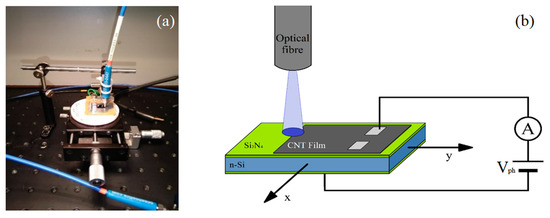
The devices were placed into a sample holder with two micrometer screw gauges that allowed precise movements in the x and y directions (Figure 1a). The light of a LED (λ = 380 nm, P = 71 µW from Ocean Optics) was directed on the devices using an optical fiber that allowed the illumination of a small circular portion of the surface with diameter of 1 mm. The electrical characterization of the devices was performed using a Keithley 236 measure unit. The measures were performed by contacting one of the top pads and the back of the devices and acquiring the I-V characteristics in the dark and under illumination (Figure 1b). After the acquisition of the I-V characteristics, looking at the voltage interval where the photocurrent took place, an appropriate voltage (Vph) at the middle of this interval was selected and applied to the devices. Keeping fixed the spatial position of the optical fiber, we moved the sample along the x and y directions, and we measured how the current changes in function of the spot position. The photocurrent Iph were calculated, using the relation: Iph = Ilight − Idark (where Ilight is the current under illumination and Idark is the current in dark). Finally, the Quantum Efficiency of each point was calculated using the relation Q.E. = (Iphhc)/ePλ, where P is the LED power and λ is the light wavelength. The obtained values were reported on a map.

Figure 1.
(a) Experimental setup: sample holder with two micrometer screw gauge that allows the movement along the x and y directions, and the optical fiber fixed above the sample. (b) Layout of the device with the setup used for the electrical characterization.
The morphology of the CNTs film of the devices was analyzed using a field emission scanning electron microscope (SEM, Zeiss Leo 1530, Zeiss, Oberkochen, Germany) at an accelerating voltage of 5 kV.
3. Results
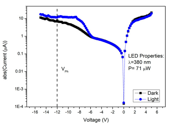
Figure 2 shows the I-V characteristic taken from the device. It shows that below −6 V, in the presence of light, the reverse current starts to increase, indicating the production of a photocurrent. The photocurrent increases linearly with the reverse bias till it reaches a plateau. That linear increase is due to the more efficient separation of the photocharge done by the higher reverse bias. When all the photocharges have been separated, the current stops increasing and reaches the plateau.

Figure 2.
I-V characteristic of the device in dark an under illumination. The value that we chose for this sample is also reported.
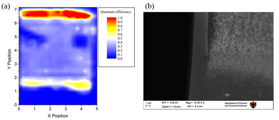
Vph was chosen at the middle of the photocurrent interval, to avoid systematic errors due to possible changes of the plateau interval during the measures. Figure 3a shows the Quantum efficiency (Q.E.) map of the device. It is possible to see that the device has a response different from zero only when the CNT film is illuminated.

Figure 3.
(a) Quantum efficiency map of our device. The device presents an average value of 0.3 but near the top and bottom edges the value increases till values near 1. (b) SEM images of the left bottom corner of the MWCNT film. The film presents two different types of edges: that at the bottom decreases gradually versus the substrate surface, while the other is sharper and is like a step.
The device presents an average Q.E. over the MWCNT film near 0.3. Over the top and bottom edges, the response is much higher, with values that reach 1. In order to understand this behavior, we looked at the MWCNT film with a scanning electron microscope. From the images we noted that the higher Q.E. is associated to region where the thickness of the CNTs film’s decrease (Figure 3b).
4. Conclusions
Photodetectors have been realized by growing MWCNTs on the surface of a n-doped silicon substrate with the top and bottom surfaces covered with a Si3N4 layer. The photoresponse of the devices has been studied across its active surface to determine possible differences of local Q.E. The measurements show that the photocurrent can be observed only if the substrate is covered by CNT. Comparing the results from the electrical measurements and the morphology of the MWCNTs film, it has been observed that a better photoresponse is associated to a lower thickness of the nanotubes film. This suggests that the thickness of the film needs to be reduced to obtain a better photoresponse from the devices.
Institutional Review Board Statement
Not applicable.
Informed Consent Statement
Not applicable.
Data Availability Statement
Data available on request.
Conflicts of Interest
The authors declare no conflict of interest.
References
- Belin, T.; Epron, F. Characterization methods of carbon nanotubes: A review. Mater. Sci. Eng. B 2005, 119, 105–118. [Google Scholar] [CrossRef]
- Poudel, Y.R.; Li, W. Synthesis, properties, and applications of carbon nanotubes filled with foreign materials: A review. Mater. Today Phys. 2018, 7, 7–34. [Google Scholar] [CrossRef]
- De Nicola, F.; Salvato, M.; Cirillo, C.; Crivellari, M.; Boscardin, M.; Passacantando, M.; Nardone, M.; De Matteis, F.; Motta, N.; De Crescenzi, M.; et al. 100% internal quantum efficiency in polychiral single-walled carbon nanotube bulk heterojunction/silicon solar cells. Carbon N. Y. 2017, 114, 402–410. [Google Scholar] [CrossRef]
- Passacantando, M.; Grossi, V.; Santucci, S. High photocurrent from planar strips of vertical and horizontal aligned multi wall carbon nanotubes. Appl. Phys. Lett. 2012, 100, 163119. [Google Scholar] [CrossRef]
- Passacantando, M.; Bussolotti, F.; Grossi, V.; Santucci, S.; Ambrosio, A.; Ambrosio, M.; Ambrosone, G.; Carillo, V.; Coscia, U.; Maddalena, P.; et al. Photoconductivity in defective carbon nanotube sheets under ultraviolet–visible–near infrared radiation. Appl. Phys. Lett. 2008, 93, 51911. [Google Scholar] [CrossRef]
- Lamura, G.; Andreone, A.; Yang, Y.; Barbara, P.; Vigolo, B.; Hérold, C.; Marêché, J.-F.; Lagrange, P.; Cazayous, M.; Sacuto, A.; et al. High-Crystalline Single- and Double-Walled Carbon Nanotube Mats Grown by Chemical Vapor Deposition. J. Phys. Chem. C 2007, 111, 15154–15159. [Google Scholar] [CrossRef]
- Coscia, U.; Ambrosone, G.; Ambrosio, A.; Ambrosio, M.; Bussolotti, F.; Carillo, V.; Grossi, V.; Maddalena, P.; Passacantando, M.; Perillo, E.; et al. Photoconductivity of multiwalled CNT deposited by CVD. Solid State Sci. 2009, 11, 1806–1809. [Google Scholar] [CrossRef]
- Tinti, A.; Righetti, F.; Ligonzo, T.; Valentini, A.; Nappi, E.; Ambrosio, A.; Ambrosio, M.; Aramo, C.; Maddalena, P.; Castrucci, P.; et al. Electrical analysis of carbon nanostructures/silicon heterojunctions designed for radiation detection. Nucl. Instrum. Methods Phys. Res. Sect. A Accel. Spectrom. Detect. Assoc. Equip. 2011, 629, 377–381. [Google Scholar] [CrossRef]
- Dekker, C. How we made the carbon nanotube transistor. Nat. Electron. 2018, 1, 518. [Google Scholar] [CrossRef]
- Hu, X.; Hou, P.; Liu, C.; Cheng, H. Carbon nanotube/silicon heterojunctions for photovoltaic applications. Nano Mater. Sci. 2019, 1, 156–172. [Google Scholar] [CrossRef]
- Manohara, H.M.; Wong, E.W.; Schlecht, E.; Hunt, B.D.; Siegel, P.H. Carbon nanotube Schottky diodes using Ti-Schottky and Pt-Ohmic contacts for high frequency applications. Nano Lett. 2005, 5, 1469–1474. [Google Scholar] [CrossRef] [PubMed]
- Melisi, D.; Nitti, M.A.; Valentini, M.; Valentini, A.; Ligonzo, T.; De Pascali, G.; Ambrico, M. Photodetectors based on carbon nanotubes deposited by using a spray technique on semi-insulating gallium arsenide. Beilstein J. Nanotechnol. 2014, 5, 1999–2006. [Google Scholar] [CrossRef] [PubMed]
- Camilli, L.; Passacantando, M. Advances on Sensors Based on Carbon Nanotubes. Chemosensors 2018, 6, 62. [Google Scholar] [CrossRef]
- Giubileo, F.; Bartolomeo, A. Di; Scarfato, A.; Iemmo, L.; Bobba, F.; Passacantando, M.; Santucci, S.; Cucolo, A.M. Local probing of the field emission stability of vertically aligned multi-walled carbon nanotubes. Carbon N. Y. 2009, 47, 1074–1080. [Google Scholar] [CrossRef]
- Passacantando, M.; Bussolotti, F.; Santucci, S.; Di Bartolomeo, A.; Giubileo, F.; Iemmo, L.; Cucolo, A.M. Field emission from a selected multiwall carbon nanotube. Nanotechnology 2008, 19, 395701. [Google Scholar] [CrossRef]
- Di Bartolomeo, A.; Scarfato, A.; Giubileo, F.; Bobba, F.; Biasiucci, M.; Cucolo, A.M.; Santucci, S.; Passacantando, M. A local field emission study of partially aligned carbon-nanotubes by atomic force microscope probe. Carbon N. Y. 2007, 45, 2957–2971. [Google Scholar] [CrossRef]
- Di Bartolomeo, A.; Giubileo, F.; Grillo, A.; Luongo, G.; Iemmo, L.; Urban, F.; Lozzi, L.; Capista, D.; Nardone, M.; Passacantando, M. Bias tunable photocurrent in metal-insulator-semiconductor heterostructures with photoresponse enhanced by carbon nanotubes. Nanomaterials 2019, 9, 1598. [Google Scholar] [CrossRef] [PubMed]
- Aramo, C.; Ambrosio, M.; Bonavolontà, C.; Boscardin, M.; Crivellari, M.; de Lisio, C.; Grossi, V.; Maddalena, P.; Passacantando, M.; Valentino, M. Large area CNT-Si heterojunction for photodetection. Nucl. Instrum. Methods Phys. Res. Sect. A Accel. Spectrom. Detect. Assoc. Equip. 2017, 845, 12–15. [Google Scholar] [CrossRef]
- Del Gobbo, S.; Castrucci, P.; Scarselli, M.; Camilli, L.; De Crescenzi, M.; Mariucci, L.; Valletta, A.; Minotti, A.; Fortunato, G. Carbon nanotube semitransparent electrodes for amorphous silicon based photovoltaic devices. Appl. Phys. Lett. 2011, 98, 183113. [Google Scholar] [CrossRef]
- Wu, Z.; Chen, Z.; Du, X.; Logan, J.M.; Sippel, J.; Nikolou, M.; Kamaras, K.; Reynolds, J.R.; Tanner, D.B.; Hebard, A.F.; et al. Transparent, Conductive Carbon Nanotube Films. Science 2004, 305, 1273–1276. [Google Scholar] [CrossRef] [PubMed]
Publisher’s Note: MDPI stays neutral with regard to jurisdictional claims in published maps and institutional affiliations. |
© 2020 by the authors. Licensee MDPI, Basel, Switzerland. This article is an open access article distributed under the terms and conditions of the Creative Commons Attribution (CC BY) license (https://creativecommons.org/licenses/by/4.0/).