Abstract
Design methods are presented for chip pulses and a constant envelope multiplexing (CEM) scheme for a new navigation satellite system in the S band. If we assume three equal-power signals are needed to transmit, the chip pulses of at least two signals can have two or more sample magnitudes for a high CEM power efficiency. Considering a case with two dual-magnitude signals, we can find the magnitude values for a target efficiency and then design the magnitude and sign patterns. We analyze the interference for all possible chip pulse sets and sorted them according to selected priorities. We also consider spectral separation between two different signal groups for a flexible operation. The design methods and the results provided in this paper can be a good reference for the signal design of a new navigation satellite system.
1. Introduction
In navigation satellite systems, except for GLONASS (Global Navigation Satellite System) and FDMA (frequency-division multiple access) [1], several independent signals are transmitted syn-chronously in time at an identical carrier frequency. They use direct-sequence spread-spectrum signals but, unlike typical wireless communication systems, the signals can have different chip rates and chip pulses [2,3,4,5,6]. Although the signals use different spreading codes, the chip pulses are designed to guarantee far lower inter- and intra-system interference. Furthermore, the signals in a frequency band are properly multiplexed to have a constant envelope, in order to maximize the power efficiency of the high-power amplifiers.
Most legacy navigation satellite signals use single-magnitude bi-phase chip pulses, so the constant envelope multiplexing (CEM) scheme can then be designed independently of the chip pulse design. On the other hand, some special requirements can unite the two designs. In this paper, we assume that three equal-power signals are transmitted and present a set of design methods for chip pulses and CEM, with example design results.
2. Design Methodology
In most cases of legacy navigation satellite systems, the signals transmitted in a frequency band have different data rates and/or target QoS’s (qualities of services), and thus have different transmit powers. In this paper, on the other hand, we assume that all the signals in a frequency band have an identical transmit power and only the data rates are determined by the target QoS’s. It is similar to the case of Galileo E5, where four signals transmitted with an identical power. But, if the number of equal power signals is three, we need some modifications or constraints in the design of the constant envelope multiplexing scheme, as well as the chip pulse waveforms.
If we simply use bi-phase chip pulse waveforms, which have a single sample magnitude, for equal power assumption, the CEM power efficiency cannot exceed 75%. That is, as much as 25% of the total transmit power is consumed in order to tailor the baseband sample constellation to have identical magnitudes. However, if we allow some of the chip pulse waveforms to have two or more magnitudes with equal average powers, the instantaneous signal powers can be different, and thus we can achieve a high CEM power efficiency. In this case, the designs of the CEM scheme and the chip pulse waveforms are tightly coupled.
In this paper, we assume to have a pair of dual-magnitude signals and a single-magnitude signal to transmit in the S band centered at 2492.028 MHz with a bandwidth 16 MHz.
2.1. Constant Envelope Multiplexing Scheme
Let us denote the three baseband signals as , , and , where the chip pulse waveforms of and have two magnitudes, and ; at an equal probability of 0.5 and is a bi-phase signal with single magnitude, . The equal average power condition requires . We further assume whenever , and vice versa, for simple design. Then, the magnitude values are determined as for a given target CEM power efficiency, with and the CEM results in [7].
2.2. Chip Pulse Waveforms
Under the constraints from the previous Section 2.1, the magnitude and sign patterns of the chip pulse waveforms are designed. With some heuristic efforts, we can employ the exhaustive search method, analyzing the interference for all possible sets of chip pulses to find the best set with the minimum worst inter- and intra-system interference. For a fast and efficient preliminary design, we can use the spectral separation coefficient (SSC) as an asymptotic metric of the interference [8].
In this paper, we sort the analysis results, first by the worst inter-system interference from a candidate signal set to the legacy signals, and then by the maximum inter-system interference from the legacy signals to the candidate signal set, and intra-system interference among the candidate signal set. The list is then investigated one by one to find the best signal set with a low out-of-band emission and transmitter and receiver complexity. If necessary, we can also apply an additional requirement that one of the three signals has its spectrum near the center of the S band, whilst the spectra of the other two are located at the outer parts of the band. The spectral separation allows for flexible operation in the inner and outer parts of the frequency band, with marginal interference between them.
3. Design Results
We performed the exhaustive analyses described in Section 2.2 with the CEM scheme in Section 2.1, for an arbitrary CEM power efficiency of , and sorted them. The list was shortened by constraining each worst SSC to not exceed the minimum worst SSC observed for all possible chip pulse waveforms by 10 dB or more.
3.1. Design Results without Spectral Separation
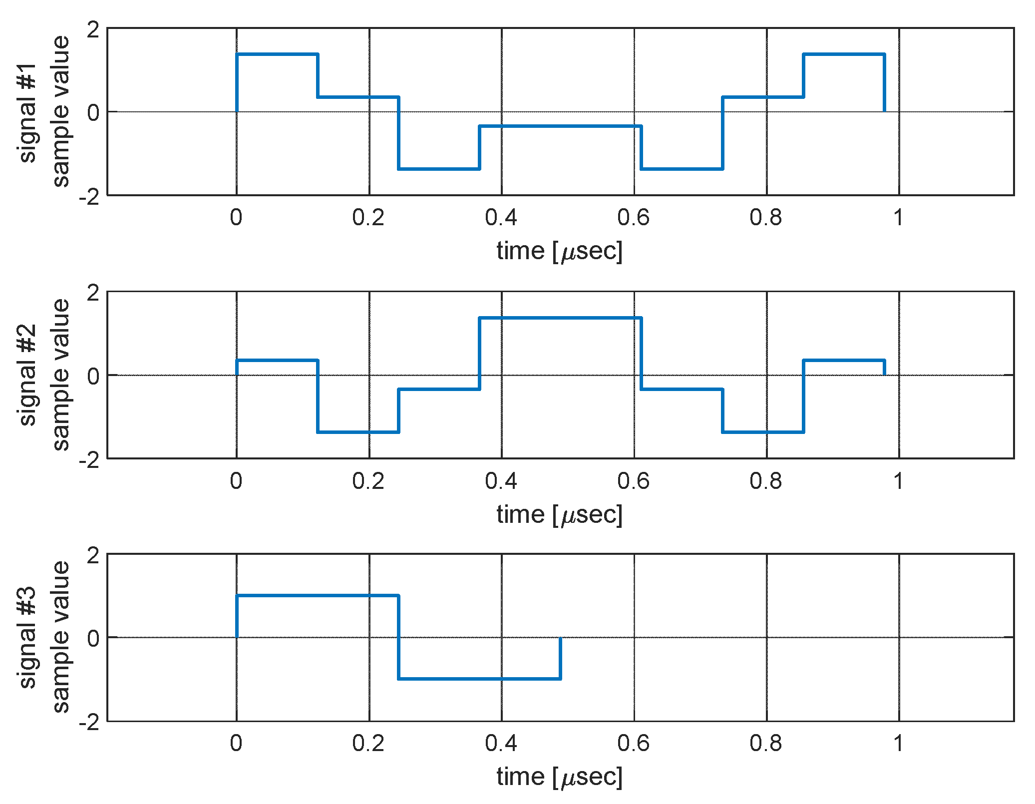
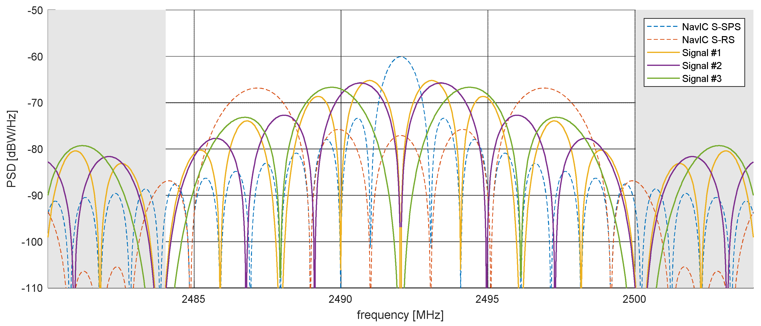
First, we searched for proper chip pulse waveforms without the requirement of separated spectra. Figure 1 and Figure 2 show the chip pulse waveforms and their spectra, designed for the case of two 1.023 Mcps signals and a 2.046 Mcps signal. The inter-system SSCs to the legacy signals are observed to be less than −74.86 dB/Hz and the inter-system SSCs from the legacy signals and the intra-system SSCs are less than −66.73 dB/Hz. For another case, with a 1.023 Mcps signal and two 2.046 Mcps signals, we found the chip pulse waveforms in Figure 3, whose spectra are shown in Figure 4. In this case, the inter-system SSCs to the legacy signals are observed to be less than −71.92 dB/Hz and the inter-system SSCs from the legacy signals and the intra-system SSCs are less than −68.27 dB/Hz.
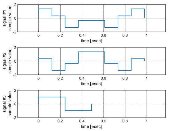
Figure 1.
Chip pulses designed for two 1.023 Mcps signals and a 2.046 Mcps signal in the S band.
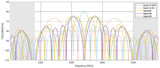
Figure 2.
PSDs (power spectral densities) of the chip pulses designed for two 1.023 Mcps signals and a 2.046 Mcps signal in the S band.3.

Figure 3.
Chip pulses designed for a 1.023 Mcps signal and two 2.046 Mcps signals in the S band.
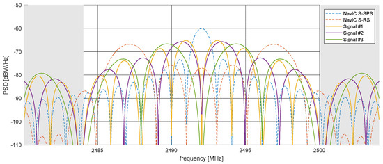
Figure 4.
PSDs of the chip pulses designed for a 1.023 Mcps signal and two 2.046 Mcps signals in the S band.
3.2. Design Results with Separated Spectra
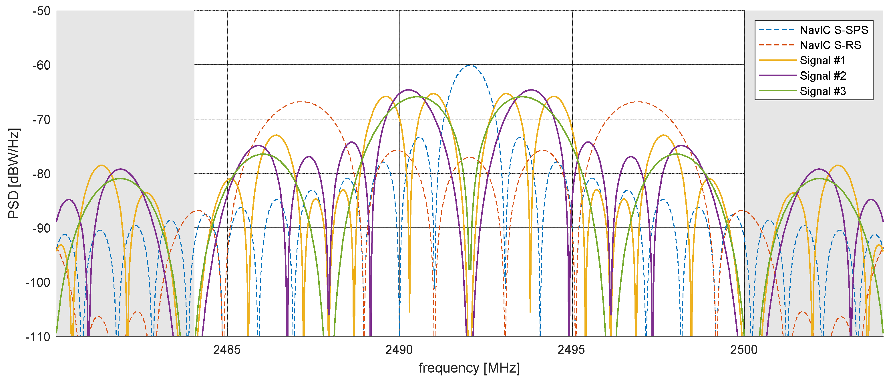
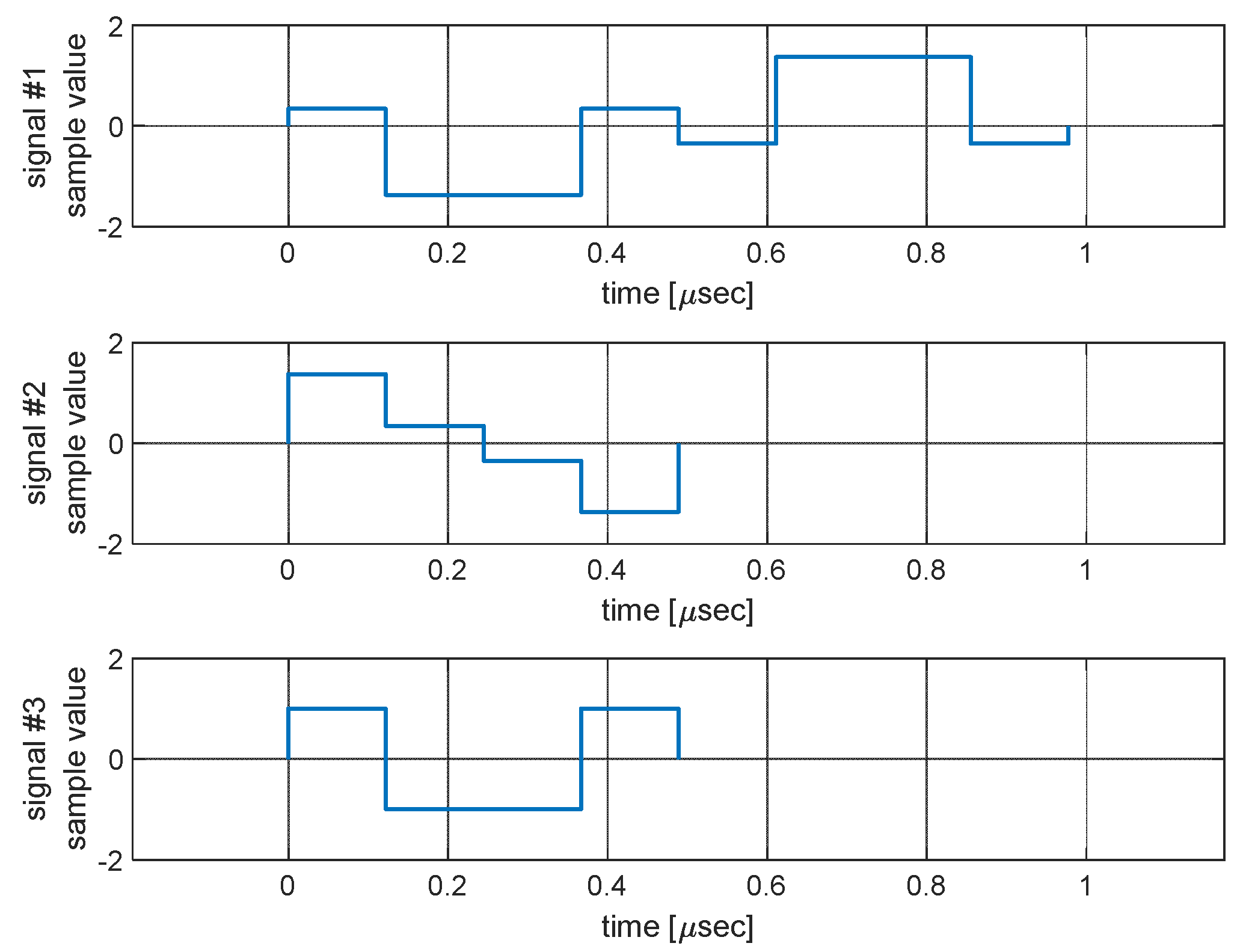
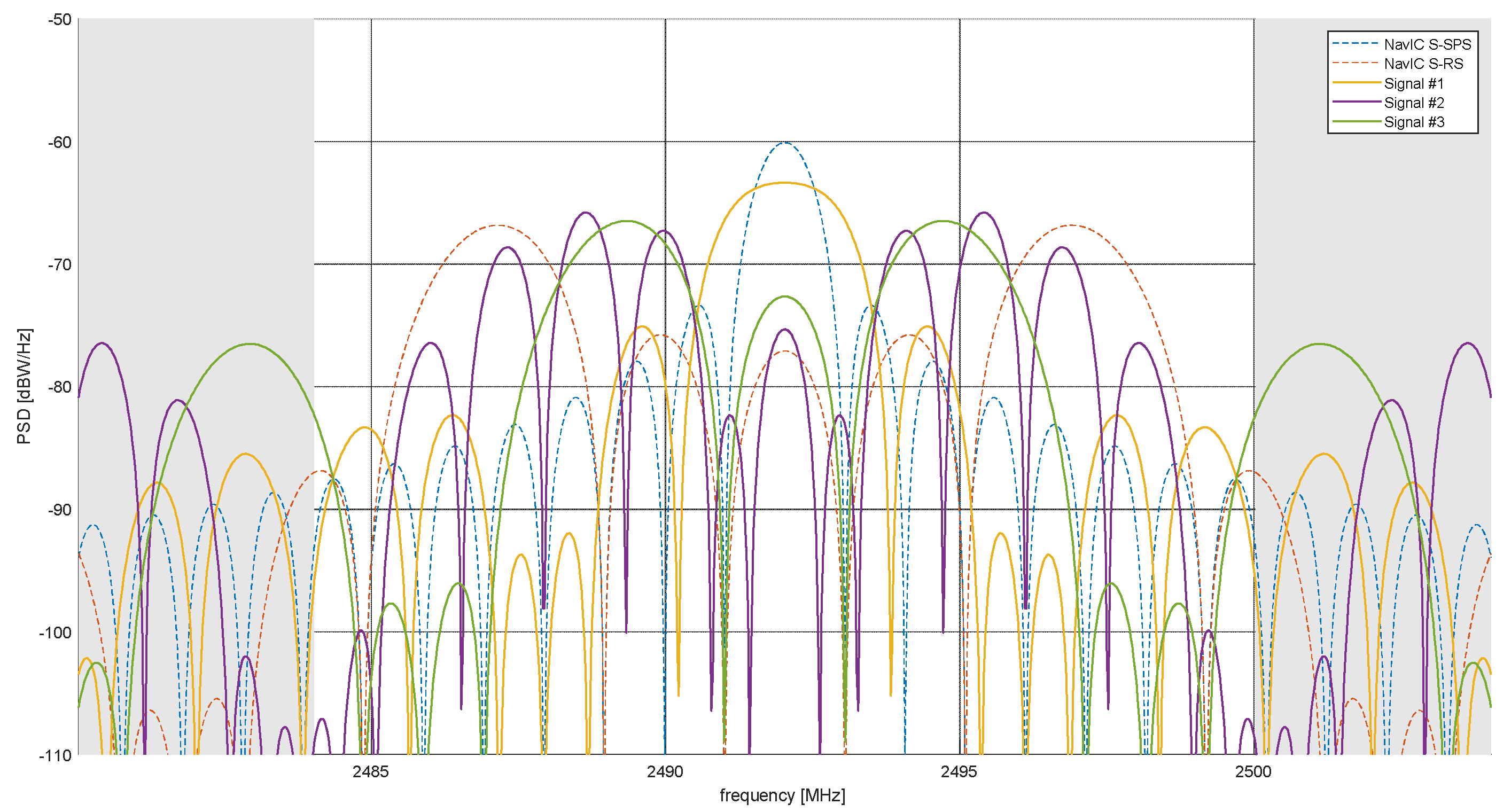
Let us assume that a signal has its spectrum in the inner band and the other two have their spectra in the outer band. Figure 5 and Figure 6 show a proper design example for the case of two 1.023 Mcps signals and a 2.046 Mcps signal. In this case, the inter-system SSCs to the legacy signals are less than −63.50 dB/Hz, whilst the inter-system SSCs from legacy and the intra-system SSCs are less than −63.85 dB/Hz. It is obvious that the requirement of separated spectra significantly reduces the degree of freedom in the design, and we can see that the worst SSCs respectively increase by 11.36 dB and 2.88 dB, in comparison with those in Section 3.1.
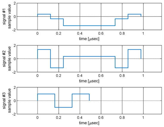
Figure 5.
Chip pulses designed for two 1.023 Mcps signals and a 2.046 Mcps signal with spectral separation in the S band.
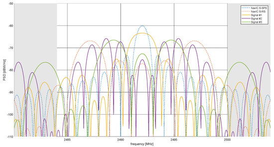
Figure 6.
PSDs of the chip pulses designed for two 1.023 Mcps signals and a 2.046 Mcps signal with spectral separation in the S band.
Unfortunately, we could not find any signal set for the case with a 1.023 Mcps signal and two 2.046 Mcps signals. That means that either the worst inter- or intra-system SSC is larger than the minimum for all possible chip pulse waveforms by 10 dB or more. In this case, we should consider loosening the worst interference requirement. Frequency division multiplexing (FDM) can be another solution. However, the FDM signals should be carefully designed to have a constant envelope, unless separate high power amplifiers are used for each signal, which is typically undesirable in practice.
4. Conclusions
A set of design methods for the chip pulses and CEM of three equal-power signals were presented. Under the condition of equal transmit powers, a pair of signals had dual magnitudes for a high CEM power efficiency. The proposed set of design methods had a high degree of freedom and thus novel sets of chip pulse waveforms could be obtained with relatively good interference performance. We designed the signals for the cases with and without the requirement of separated signal spectra and found that the worst interferences can significantly increase with spectral separation. The design methods presented in this paper and the design results can be a good reference for planning a new navigation satellite system, including the future Korea Positioning System.
Funding
This research was funded by Electronics and Telecommunications Research Institute (ETRI), grant number 23ZH1100 (Study on 3D communication technology for hyper-connectivity).
Institutional Review Board Statement
Not applicable.
Informed Consent Statement
Not applicable.
Data Availability Statement
Data are available in this manuscript.
Conflicts of Interest
The author declares no conflict of interest.
References
- GLONASS Documents. Available online: http://www.glonass-svoevp.ru/index.php?option=com_content&view=article&id=146&Itemid=305&lang=en (accessed on 18 May 2023).
- GPS Interface Control Documents. Available online: https://www.gps.gov/technical/icwg/ (accessed on 18 May 2023).
- Galileo Programme Reference Documents. Available online: https://www.gsc-europa.eu/electronic-library/programme-reference-documents#Galileopub (accessed on 18 May 2023).
- BeiDou Navigation Satellite System ICDs. Available online: http://en.beidou.gov.cn/SYSTEMS/ICD/ (accessed on 18 May 2023).
- IRNSS Signal-in-Space Interface Control Document ICD Ver 1.1. Available online: https://www.isro.gov.in/IRNSSSignal.html (accessed on 18 May 2023).
- Quasi-Zenith Satellite System (QZSS). Available online: https://qzss.go.jp/en/technical/ps-is-qzss/ps-is-qzss.html (accessed on 18 May 2023).
- Lim, H.; Lee, S.U. Constant Envelope Multiplexing Scheme for Three Equal Power Signals. In Proceedings of the APCC, Jeju, Rpublic of Korea, 19–21 October 2022. [Google Scholar]
- Betz, J.W. Effect of Partial-Band Interference on Receiver Estimation of C/N0: Theory. In Proceedings of the ION-NTM, Long Beach, CA, USA, 22–24 January 2001. [Google Scholar]

Disclaimer/Publisher’s Note: The statements, opinions and data contained in all publications are solely those of the individual author(s) and contributor(s) and not of MDPI and/or the editor(s). MDPI and/or the editor(s) disclaim responsibility for any injury to people or property resulting from any ideas, methods, instructions or products referred to in the content. |
© 2023 by the author. Licensee MDPI, Basel, Switzerland. This article is an open access article distributed under the terms and conditions of the Creative Commons Attribution (CC BY) license (https://creativecommons.org/licenses/by/4.0/).