
Confinement Specific Design of SOI Rib Waveguides with Submicron Dimensions and Single-Mode Operation †

 , ,
, ,
Abstract
:1. Introduction
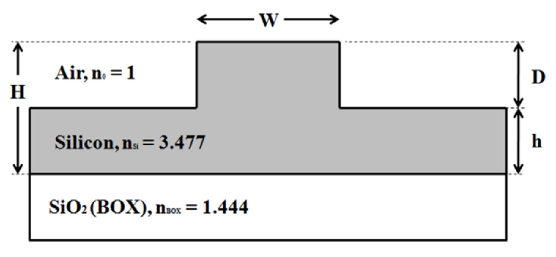
2. Methodology
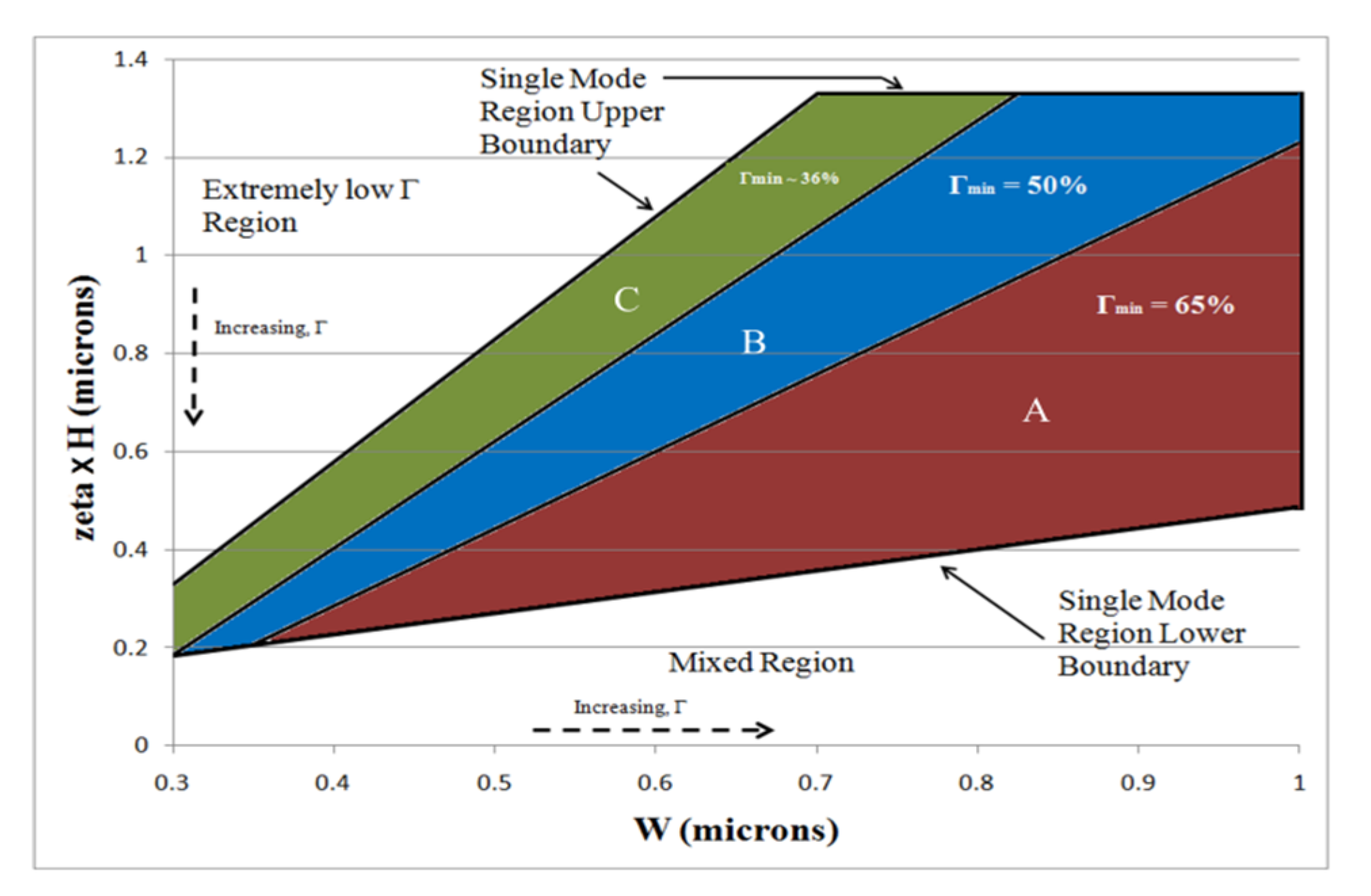
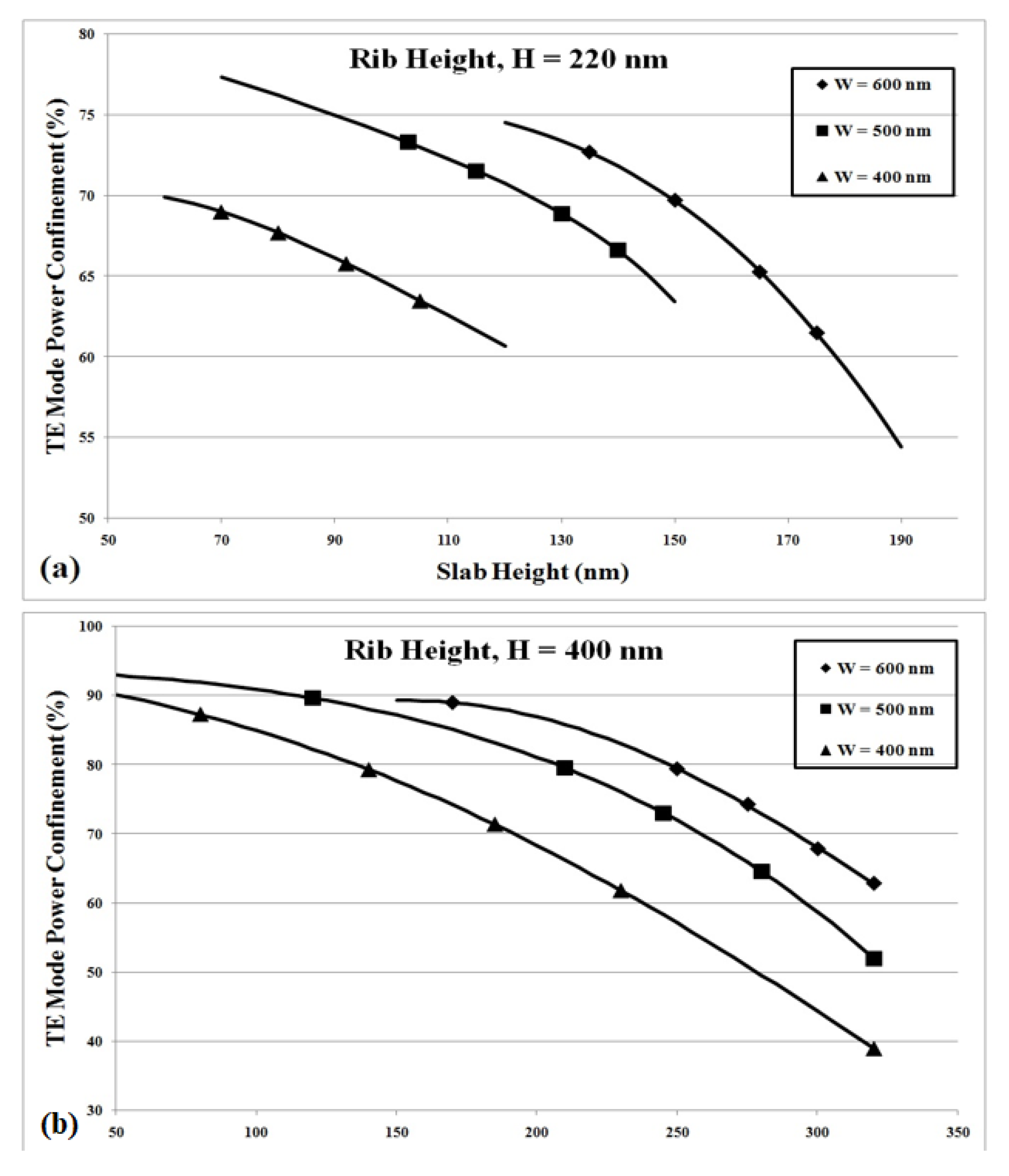
3. Results and Discussion
4. Conclusions
Author Contributions
Funding
Data Availability Statement
Conflicts of Interest
References
- Shaikh, A.J.; Packeer, F.; Baig, M.M.A.; Sidek, O. A full 3D model of the modulation efficiency of a submicron complementary metal–oxide–semiconductor (CMOS)-compatible interleaved-junction optical phase shifter. J. Comput. Electron. 2019, 18, 1379–1387. [Google Scholar] [CrossRef]
- Shaikh, A.J.; Packeer, F.; Baig, M.M.A.; Sidek, O. Rigorous 3D Model of Capacitance of CMOS Compatible Optical Phase Shifters Based on Interleaved Junctions with Submicron Dimensions. J. Nanoelectron. Optoelectron. 2020, 15, 1209–1215. [Google Scholar]
- Shaikh, A.J.; Packeer, F.; Sidek, O. Self phase modulation and cross phase modulation in nonlinear silicon waveguides for on-chip optical networks—A tutorial. Nano Commun. Netw. 2017, 14, 60–67. [Google Scholar] [CrossRef]
- Shaikh, A.J.; Sidek, O. Making Silicon Emit Light Using Third Harmonic Generation. Procedia Eng. 2012, 29, 1456–1461. [Google Scholar] [CrossRef] [Green Version]
- Shaikh, A.J.; Sidek, O. Holistic Analysis and Systematic Design of High Confinement Factor, Single Mode, Nanophotonic Silicon-on-Insulator Rib Waveguides. J. Nanoelectron. Optoelectron. 2017, 12, 381–391. [Google Scholar] [CrossRef]
- Soref, R.A.; Schmidtchen, J.; Petermann, K. Large single-mode rib waveguides in GeSi-Si and Si-on-SiO2. IEEE J. Quantum Electron. 1991, 27, 1971–1974. [Google Scholar] [CrossRef]
- Xia, J.; Yu, J.; Li, Y.; Chen, S. Single-mode condition for silicon rib waveguides with large cross sections. OPTICE 2004, 43, 1953–1954. [Google Scholar] [CrossRef] [Green Version]
- de Laurentis, M.; Irace, A.; Breglio, G. Determination of single mode condition in dielectric rib waveguide with large cross section by finite element analysis. J. Comput. Electron. 2007, 6, 285–287. [Google Scholar] [CrossRef]
- Pogossian, S.P.; Vescan, L.; Vonsovici, A. The single-mode condition for semiconductor rib waveguides with large cross section. J. Lightwave Technol. 1998, 16, 1851–1853. [Google Scholar] [CrossRef]
- Lousteau, J.; Furniss, D.; Seddon, A.B.; Benson, T.M.; Vukovic, A.; Sewell, P. The single-mode condition for silicon-on-insulator optical rib waveguides with large cross section. J. Lightwave Technol. 2004, 22, 1923–1929. [Google Scholar] [CrossRef]
- Seong Phun, C.; Ching Eng, P.; Soon Thor, L.; Reed, G.T.; Passaro, V.M.N. Single-mode and polarization-independent silicon-on-insulator waveguides with small cross section. J. Lightwave Technol. 2005, 23, 2103–2111. [Google Scholar] [CrossRef]
- Dai, D.; Sheng, Z. Numerical analysis of silicon-on-insulator ridge nanowires by using a full-vectorial finite-difference method mode solver. J. Opt. Soc. Am. B 2007, 24, 2853–2859. [Google Scholar] [CrossRef]


| H = 220 nm | |
| W = 600 nm | |
| W = 500 nm | |
| W = 400 nm | |
| H = 400 nm | |
| W = 600 nm | |
| W = 500 nm | |
| W = 400 nm | |
Publisher’s Note: MDPI stays neutral with regard to jurisdictional claims in published maps and institutional affiliations. |
© 2022 by the authors. Licensee MDPI, Basel, Switzerland. This article is an open access article distributed under the terms and conditions of the Creative Commons Attribution (CC BY) license (https://creativecommons.org/licenses/by/4.0/).
Share and Cite
Shaikh, A.J.; Abro, A.G.; Baig, M.M.A.; Siddiqui, M.A.A.; Abbas, S.M. Confinement Specific Design of SOI Rib Waveguides with Submicron Dimensions and Single-Mode Operation. Eng. Proc. 2022, 20, 19. https://doi.org/10.3390/engproc2022020019
Shaikh AJ, Abro AG, Baig MMA, Siddiqui MAA, Abbas SM. Confinement Specific Design of SOI Rib Waveguides with Submicron Dimensions and Single-Mode Operation. Engineering Proceedings. 2022; 20(1):19. https://doi.org/10.3390/engproc2022020019
Chicago/Turabian StyleShaikh, Abdurrahman Javid, Abdul Ghani Abro, Mirza Muhammad Ali Baig, Muhammad Adeel Ahmad Siddiqui, and Syed Mohsin Abbas. 2022. "Confinement Specific Design of SOI Rib Waveguides with Submicron Dimensions and Single-Mode Operation" Engineering Proceedings 20, no. 1: 19. https://doi.org/10.3390/engproc2022020019
APA StyleShaikh, A. J., Abro, A. G., Baig, M. M. A., Siddiqui, M. A. A., & Abbas, S. M. (2022). Confinement Specific Design of SOI Rib Waveguides with Submicron Dimensions and Single-Mode Operation. Engineering Proceedings, 20(1), 19. https://doi.org/10.3390/engproc2022020019