Abstract
The Hall effect is widely used in magnetic field sensors and contactless measurement systems. Accurate modeling of Hall-effect elements is essential for optimizing performance, especially in high-sensitivity applications under controlled conditions like vacuum. This paper introduces a graphical software tool for calculating key electrical parameters of Hall elements, such as Hall voltage, Hall coefficient, and carrier mobility. Users can input variables like semiconductor thickness, current, and magnetic field, with built-in models for materials like silicon, germanium, and gallium arsenide. Designed for vacuum operation, the tool supports simulation-based analysis, aiding researchers and educators in understanding and evaluating Hall-effect devices.
1. Introduction
The Hall element is a fundamental semiconductor structure utilized for the measurement of magnetic fields based on the Hall effect—discovered by Edwin Hall in 1879. When an electric current flows through a conductive material in the presence of a perpendicular magnetic field, a transverse voltage—known as the Hall voltage—is generated. This principle is widely exploited in various applications including magnetic field sensing, current measurement, and contactless position detection. As Hall-based sensors become increasingly prevalent in modern electronic systems, especially in automotive, aerospace, and industrial automation domains, the accurate estimation of their electrical parameters becomes crucial. Key quantities such as the Hall voltage, Hall coefficient, and carrier mobility are highly dependent on the material properties, device geometry, and environmental conditions—particularly under vacuum, where surface contamination and extrinsic effects are minimized. Despite the availability of theoretical models, there is a lack of user-friendly computational tools that enable engineers and researchers to simulate and analyse the behaviour of Hall elements under various input conditions. A dedicated software environment that accounts for different semiconductor materials, physical dimensions, and external field strengths can significantly enhance the design and educational processes related to Hall-effect devices. This paper presents the design and implementation of a lightweight graphical software application for evaluating the key electrical parameters of a Hall element. The application allows users to specify the thickness of the semiconductor layer, the current through the device, and the applied magnetic field. It includes predefined models for commonly used materials such as germanium, silicon, and gallium arsenide, incorporating their intrinsic carrier concentrations and resistivity values [1,2].
The primary objective of this work is to develop a simulation tool suitable for both academic and engineering environments, which facilitates intuitive exploration of Hall-effect behaviour. The main contributions of this study are as follows: a computational model for calculating Hall voltage, Hall coefficient, and carrier mobility under vacuum conditions-: a graphical interface that enables parameter selection and real-time computation-: integration of material-specific properties enabling comparative analysis across different semiconductor types [3,4].
2. Methodology
2.1. Software Architecture
The developed application follows a modular architecture, organized into four main components (Figure 1):
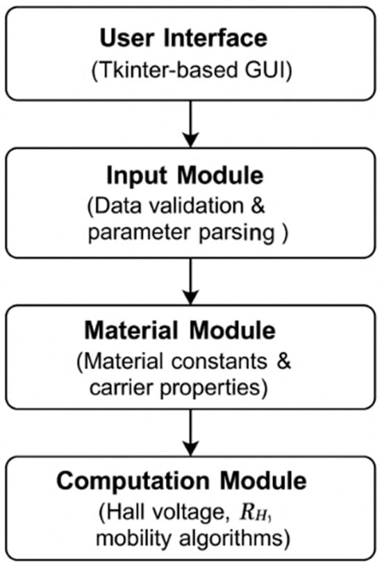
Figure 1.
Program algorithm of the simulation tool.
Input Module—handles user-provided parameters including current, magnetic field, and semiconductor thickness;
Material Module—contains predefined physical constants for selected materials such as germanium (Ge), silicon (Si), and gallium arsenide (GaAs);
Computation Module—performs calculations of the Hall voltage, Hall coefficient, and carrier mobility using standardized physical models;
User Interface Module—provides a graphical interface for parameter selection, calculation triggering, and real-time result display.
The modules interact through well-defined internal APIs, ensuring separation of concerns and code maintainability.
2.2. Computational Models
The software uses classical analytical expressions based on the Hall effect and semiconductor physics. The Hall voltage VH is computed as
where I is the applied current, B is the magnetic flux density, q is the elementary charge, n is the carrier concentration, and d is the semiconductor thickness.
The Hall coefficient RH is derived as:
Carrier mobility μ is estimated from:
where ρ is the material resistivity. All computations assume vacuum conditions, minimizing environmental interference.
2.3. Development Environment
The software was developed in Python 3.11 using the Tkinter library for graphical interface design (Figure 2). The project utilizes modular programming techniques and is packaged using PyInstaller 6.15.0 to generate a standalone executable file compatible with Windows operating systems [5].
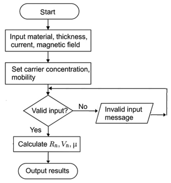
Figure 2.
Algorithm of the code.
2.4. User Interface and Functionality
The graphical user interface is designed to support intuitive interaction. It includes dropdown menus for material selection, text fields for parameter input, and buttons to initiate calculations. The result area displays computed values with appropriate units and precision. The interface ensures real-time feedback and error handling for invalid input.
2.5. Data Input Process
Users are required to input the following parameters (Figure 3):
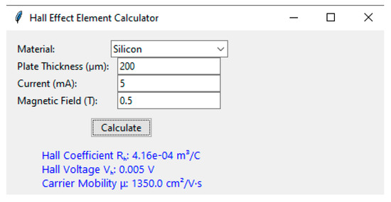
Figure 3.
User interface screenshot displaying results from entered data.
- Thickness of the semiconductor layer in micrometers (µm);
- Applied current in milliamperes (mA);
- Magnetic field strength in teslas (T);
- Material selection, via dropdown list (Ge, Si and GaAs).
Upon input validation, these values are passed to the computation module, which returns the calculated Hall voltage, Hall coefficient, and carrier mobility in both SI- and CGS-compatible units (Figure 4).
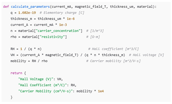
Figure 4.
Part of the code of the Hall element simulation tool.
3. Validation and Verification
3.1. Validation Methodology
To ensure the accuracy and reliability of the developed software, a multi-stage validation strategy was adopted. The approach includes:
Comparison with Analytical Solutions—All computed parameters—including Hall voltage VH, Hall coefficient RH, and carrier mobility μ —were validated against analytical expressions from classical semiconductor theory. The formulas used in the software were verified symbolically using reference materials [6,7].
Cross-Validation with Numerical Simulation Tools—Simulated values from the developed tool were compared to results obtained using commercial semiconductor simulation software (e.g., COMSOL Multiphysics 6.1, SILVACO ATLAS 5.38) for identical input parameters. Boundary conditions were kept consistent, and the models were set to simulate steady-state conditions under vacuum.
Comparison with Experimental Data—A small set of reference experimental measurements from published studies [8] was used for comparison. These included Hall voltage values obtained under known material properties and controlled magnetic fields for silicon and germanium samples.
3.2. Validation Results
The validation process yielded consistent results across all three methods:
The absolute deviation between the software output and analytical calculations was less than 0.5% across all tested configurations. Numerical simulation tools yielded maximum relative error below 1.2%, primarily due to meshing granularity and boundary approximations. Comparisons with experimental data showed agreement within 5%, which is acceptable given the known tolerances in sample fabrication and environmental influence even under vacuum. Table 1 summarizes a representative comparison between analytical results and software output (Figure 5).

Table 1.
Comparison of Computed and Analytical Hall Voltages.
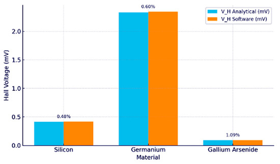
Figure 5.
Comparison of analytical and software voltages.
Calculations were performed using the developed software to determine the electrophysical parameters of a thin semiconductor wafer made of gallium arsenide (GaAs) with a thickness of 0.056 µm. Gallium arsenide is widely used in microelectronics and optoelectronics due to its high charge carrier mobility and excellent performance at high frequencies. During the analysis, the values of the Hall voltage were evaluated as a function of the magnetic field intensity under a constant current applied to the wafer. It was established that the Hall voltage varies in the range from 27 mV to 265 mV (Figure 6 and Figure 7), reflecting the material’s sensitivity to external magnetic influences and confirming its applicability in sensor and high-frequency devices [9].
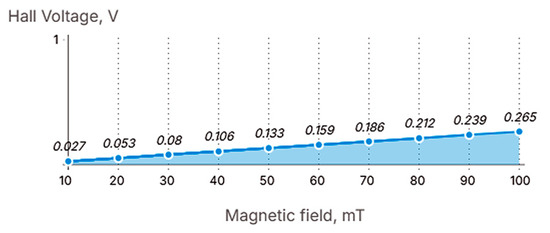
Figure 6.
Dependence of Hall Voltage on Magnetic Field, GaAs plate.
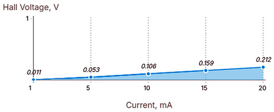
Figure 7.
Dependence of Hall Voltage on current, GaAs plate.
The graph clearly demonstrates a direct and almost perfectly linear relationship between the applied current and the generated Hall voltage. This is characteristic behavior for the Hall effect in a constant magnetic field and for a given Hall coefficient of the material. The slope of the line represents the proportionality constant, often related to the Hall resistance or Hall coefficient.
This linear dependency confirms the expected behavior of the Hall effect in a semiconductor wafer under constant current. The Hall voltage is directly proportional to the magnetic field intensity. The graph confirms a stable and linear sensitivity of the tested material (presumably GaAs) to the magnetic field, making it suitable for application in precision magnetic field sensing devices.
3.3. Error Sources and Analysis
The main sources of error were attributed to: precision loss during floating-point arithmetic in Python; idealized material models, assuming temperature-independent constants and perfect vacuum conditions; limited resolution in user-provided inputs and GUI rounding behavior. Despite these factors, the software maintains a high level of precision, and the deviations are within acceptable engineering limits for both academic and prototyping purposes. The measurement results of the germanium plate parameters are summarized in Table 2.
Table 2.
Experimental results, Ge plate.
In previous studies, the development and analysis of a computational system for evaluating the electrical parameters of Hall-effect sensors were presented (Figure 8 and Figure 9) [9]. These studies detailed the software architecture, including the mathematical models and algorithms used to compute key parameters such as the Hall coefficient, Hall voltage, and carrier mobility.
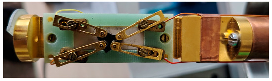
Figure 8.
Ge plate, used in measurement system DX50.
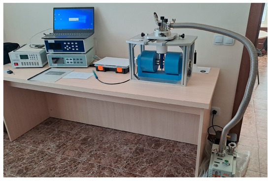
Figure 9.
Measurement setup DX50 employed in a previous study for Hall effect characterization.
Additionally, the user interface and the data input methodology—covering geometric dimensions, applied current, and magnetic field strength—were discussed. The present work builds upon this foundation by extending the software’s capabilities through the integration of validation and verification modules. These enhancements enable systematic comparison of software-generated results with analytical solutions, numerical simulations, and experimental measurements. Furthermore, the user interface has been redesigned in English to increase accessibility for the international research community.
Previous studies have shown that increasing the magnetic field leads to an increase in charge carrier mobility. Different semiconductor materials exhibit significant variation in their Hall coefficient values. The germanium sample demonstrates higher Hall coefficient values compared to gallium arsenide, which can be attributed to the lower carrier mobility in the latter. Reduced carrier mobility limits the induced voltage, consequently resulting in lower Hall coefficient values.
The accuracy of the results has been substantiated through validation against prior experimental data, demonstrating consistency between measured and calculated values. Minor deviations observed during computation are primarily attributed to the precision of the input parameters, particularly the current and magnetic field measurements. Through these advancements, the current work offers a significant contribution to existing tools for Hall-effect sensor analysis, providing broader applicability for research, education, and industrial deployment in the field of semiconductor device and sensor technology.
4. Conclusions
This paper presented the design, development, and validation of a computational software tool for the analysis of Hall-effect element parameters under vacuum conditions. The tool provides a flexible and material-aware environment for evaluating the Hall voltage, Hall coefficient, and carrier mobility in semiconductor thin films made of silicon, germanium, or gallium arsenide. Emphasis was placed on the integration of accurate analytical models, user-friendly input configuration, and dynamic output visualization. The software’s modular architecture enables efficient data processing and supports the extension of material databases and computational models. Validation results demonstrated a high level of agreement with both analytical calculations and results from commercial simulation tools, while experimental comparisons further confirmed the software’s applicability in practical contexts.
The system proves useful for both engineering applications and academic research. It allows rapid testing of input parameters and exploration of Hall-effect behaviour under various physical conditions. Its intuitive interface makes it suitable for educational use in electronics and solid-state physics curricula. The presented tool offers a significant contribution toward the accurate and accessible study of Hall-effect phenomena in modern semiconductor technology.
Author Contributions
Conceptualization, G.M. and G.G.; methodology, G.G.; software, G.M.; formal analysis, G.G.; investigation, G.M.; resources, G.G.; data curation, G.M.; writing—original draft preparation, G.M.; writing—review and editing, G.G.; visualization, G.M.; All authors have read and agreed to the published version of the manuscript.
Funding
This work is funded by the Bulgarian Ministry of Education and Science under the National Program “Young Scientists and Postdoctoral Researchers–2”.
Institutional Review Board Statement
Not applicable.
Informed Consent Statement
Not applicable.
Data Availability Statement
Dataset available on request from the author.
Conflicts of Interest
The authors declare no conflicts of interest.
References
- Lozanova, S.; Ralchev, M.; Roumenin, C. Device for Semiconductor Carrier Mobility Measurement, C.R. Acad. Bulg. Sci. 2022, 75, 1334–1342. [Google Scholar] [CrossRef]
- Lozanova, S.V.; Roumenin, C.S. Silicon Hall-effect Multisensor. In Proceedings of the 2020 XI National Conference with International Participation (ELECTRONICA), Sofia, Bulgaria, 23–24 July 2020; pp. 1–4. [Google Scholar] [CrossRef]
- Wang, X.; Zhou, R.; Zhang, Y.; Fan, X. Semiconductor electrical parameter measurement based on Hall effect and the improved mobility spectrum algorithm. Measurement 2024, 238, 115257. [Google Scholar] [CrossRef]
- Ramalho, L. Fluent Python: Clear, Concise, and Effective Programming, 1st ed.; O’Reilly Media: Sebastopol, CA, USA, 2015. [Google Scholar]
- Sze, S.M.; Ng, K.K. Physics of Semiconductor Devices, 3rd ed.; Wiley-Interscience: Hoboken, NJ, USA, 2006. [Google Scholar]
- Streetman, B.G.; Banerjee, S. Solid State Electronic Devices, 7th ed.; Pearson: Boston, MA, USA, 2015. [Google Scholar]
- Kelemenová, T.; Kelemen, M.; Virgala, I.; Miková, Ľ.; Frankovský, P.; Lörinc, M.; Lipták, T.; Sedlačko, P. Experimental Verification of Hall Effect Sensor Properties. J. Autom. Control. 2015, 3, 75–78. [Google Scholar]
- Friedemann, S.; Wirth, S.; Oeschler, N.; Krellner, C.; Geibel, C.; Steglich, F.; MaQuilon, S.; Fisk, Z.; Paschen, S. Hall effect measurements and electronic structure calculations and its reference compounds LuRh2Si2 and YbIr2Si2. Phys. Rev. B 2010, 82, 035103. [Google Scholar] [CrossRef]
- Mironova, G.; Goranov, G. Analysis of the electrical characteristics of Hall elements made of Germanium and Gallium Arsenide. In Proceedings of the 2024 9th International Conference on Energy Efficiency and Agricultural Engineering (EE&AE), Ruse, Bulgaria, 27–29 June 2024; pp. 1–4. [Google Scholar] [CrossRef]


Disclaimer/Publisher’s Note: The statements, opinions and data contained in all publications are solely those of the individual author(s) and contributor(s) and not of MDPI and/or the editor(s). MDPI and/or the editor(s) disclaim responsibility for any injury to people or property resulting from any ideas, methods, instructions or products referred to in the content. |
© 2025 by the authors. Licensee MDPI, Basel, Switzerland. This article is an open access article distributed under the terms and conditions of the Creative Commons Attribution (CC BY) license (https://creativecommons.org/licenses/by/4.0/).