Abstract
Additive Manufacturing (AM) and printing-based fabrication technologies have emerged as powerful enablers for next-generation electronic integration and packaging, addressing the growing limitations of conventional subtractive manufacturing techniques. As electronic systems continue to scale toward higher operating frequencies (10–110 GHz and beyond) and increased functional density (>104 interconnects/cm2), traditional packaging approaches struggle with rigid design constraints, complex processing steps (>15–25 fabrication steps), high tooling costs ($10,000–$100,000 for mask and molds) and limited compatibility with heterogeneous integration. In this review, a comprehensive and critical overview of major additive manufacturing and printing technologies including aerosol jet printing, inkjet printing, vat polymerization, fused filament fabrication (FFF) and nScrypt printing is presented from the perspective of electronic assembly and packaging. The fundamental working mechanisms, material compatibility, resolution limits, scalability, and reliability considerations of each technique are systematically discussed. From a manufacturing standpoint, AM reduces material waste by 50–90% compared to subtractive PCB processing and eliminates tooling costs, enabling low-volume prototyping with per-unit fabrication costs reduced by 30–70% for small batches (<100 units). Production throughput varies widely, from 1 to 20 cm2/min for high-resolution direct write systems to >100 cm2/min for scalable inkjet systems. Moreover, it is discussed how these technologies enable advanced packaging architectures such as printed signal crossovers, three-dimensional interconnects, ramps, and embedded chip assemblies. Recent research efforts and reported demonstrations are analyzed to highlight the advantages and current limitations of additive manufacturing for high-frequency, RF, and system-on-package (SoP) applications. Finally, future directions and remaining challenges are discussed, including advances in materials, custom and on-demand manufacturing, enhanced design freedom, integration of multifunctionality, cost-effectiveness, and smart packaging solutions. This review aims to serve as a reference for researchers and engineers seeking to leverage additive manufacturing for high-performance electronic integration and next-generation electronic packaging solutions.
1. Introduction
The continuous scaling of electronic systems towards higher functionality, increased operating frequencies, and reduced form factors has placed unprecedented demands on electronic integration and packaging technologies [1,2,3,4]. While semiconductor device fabrication has advanced rapidly, conventional electronic packaging methods such as wire bonding [5], flip-chip interconnects [6], and multilayer printed circuit boards [7] are increasingly constrained by parasitic effects, rigid design rules, complex processing steps, and escalating manufacturing costs [8,9,10,11]. These challenges are particularly pronounced in emerging application domains including millimeter-wave (mm-wave) communication, 5G and beyond wireless systems, power electronics, and heterogeneous integration, where electrical, thermal, and mechanical performance must be simultaneously optimized within compact volumes [12,13,14].
Electronic packaging is no longer a passive mechanical enclosure, but an active system-level technology that directly influences signal integrity, power handling, thermal dissipation, and long-term reliability [15,16]. Traditional subtractive manufacturing approaches rely on masks, etching, drilling, and lamination, which limit geometric freedom and hinder rapid design iteration. Furthermore, these processes often require multiple fabrication steps and materials that are not easily compatible with advanced three-dimensional (3D) integration strategies [17]. As a result, there is a growing need for alternative manufacturing paradigms that can enable fine-pitch interconnects, embedded components, and customized package architectures while reducing cost, material waste, and development time [18].
Additive Manufacturing (AM) and printing-based fabrication technologies have emerged as transformative tools capable of addressing many of these limitations [19,20,21,22]. Unlike conventional manufacturing, AM enables the direct, maskless and digitally controlled deposition of functional materials including conductive, dielectrics, and structural polymers onto planar and nonplanar substrates. There are total of seven types of AM techniques, [23] but in this article we discussed five printing technologies, such as aerosol jet printing [2,24], inkjet printing [25,26], vat polymerization [27,28], fused filament fabrication (FFF), also called fused deposition modeling (FDM) [29,30] and fluid-dispensing-based nScrypt printing [31,32], as mentioned in Figure 1, which allows the fabrication of electrical interconnects, dielectric structures, and mechanical supports with a level of design freedom unattainable using traditional approaches.
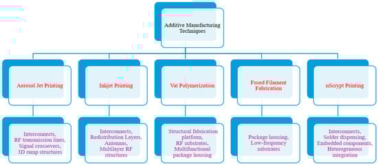
Figure 1.
The schematic shows AM techniques for electronic integration and packaging.
In recent years, these technologies have transitioned from simple prototyping tools to viable manufacturing platforms for printed electronics, system-on-package (SoP) architectures, embedded-chip assemblies, and smart electronic packaging. Numerous studies have demonstrated their effectiveness in fabricating printed antennas, RF transmission lines, signal crossovers, three-dimensional ramp interconnects, and embedded passive and active components (demonstration shown in Figure 2). Importantly, additive manufacturing enables heterogeneous integration by allowing materials with vastly different electrical, thermal, and mechanical properties to be combined within a single package [11,33,34,35].
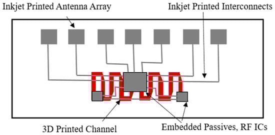
Figure 2.
Demonstration of AM-printed antennas, interconnects, and embedded chips on flexible substrate.
The primary motivation of this review is to provide a comprehensive and critical overview of additive manufacturing and printing technologies specifically from the perspective of electronic integration and packaging. Rather than treating these techniques as isolated fabrication tools, this article evaluates how different printing methods operate, their material compatibility, resolution limits, scalability, reliability, and how they can be strategically combined to enable advanced electronic packaging solutions. The key focus is placed on applications such as printed signal crossovers, three-dimensional interconnects, ramp-based packaging topologies, and chip-embedded assemblies, which represent key enabling technologies for next-generation electronic systems. By integrating recent research developments and experimental demonstrations, this review serves as a comprehensive reference for researchers and engineers pursuing additive manufacturing approaches for high-performance electronic integration and packaging.
2. Printing Technology
2.1. Aerosol Jet Printing
Aerosol jet printing is one of many direct-write (DW) processes. Direct-write technology refers to the creation of micro- and nanoscale, 2D or 3D structures on flat or nonconformal surfaces. The AJP process can print a variety of aerosolization-capable liquid inks such as colloidal inks, nanoparticle inks, diluted thick film paste and UV-curable polymer solutions [36]. Figure 3 shows a conceptual layout of aerosol jet printing apparatus. Liquid inks are first atomized to create a dense aerosol cloud of 1–5 µm diameter droplets. A pneumatic nebulizer is typically used when the liquid viscosity is in the range of 20–1000 cP and an ultrasonic atomizer is used for low viscosity fluids, i.e., 1–20 cP. The particle diameter is limited to below 1 µm for the pneumatic nebulizer and below 0.2 µm for the ultrasonic atomizer. Once created, a carrier gas transfers the aerosol to a printing head. This carrier gas is typically dry with nitrogen, but other gases and vapors can be introduced into the gas stream as needed. Within the printhead, a second co-flowing sheath gas focuses the droplets to a 10–100 µm diameter jet. The droplets (shown in red color in Figure 3) exit the nozzle at velocities up to 100 m/s [25,37,38].
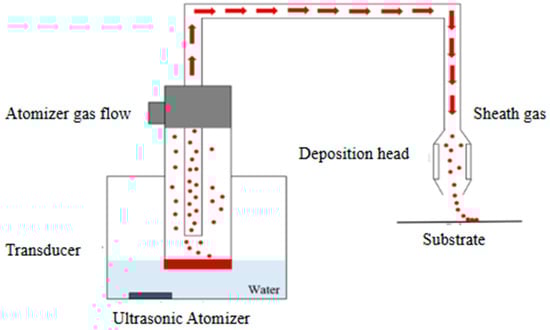
Figure 3.
Working principle of aerosol jet printing for precision electronic fabrication.
2.1.1. Advantages and Disadvantages
AJP offers exceptional flexibility in terms of printable materials, supporting a wide viscosity range and allowing for the deposition of nanoparticle-based conductive, dielectrics polymers and functional composites. Its non-contact nature enables printing on fragile substrates, previously fabricated components, and nonplanar surfaces without mechanical damage. The fine resolution and three-dimensional deposition capability make AJP particularly well-suited for fabricating vertical interconnects, dielectric ramps, and conformal conductive traces. Additionally, the use of sheath gas reduces nozzle clogging and enhances process stability, which is critical for repeatable micro-scale printing [24,39].
Despite its strengths, AJP faces challenges related to throughput and scalability. The focused aerosol jet inherently limits the deposition rate, making large area printing time consuming. Equipment complexity and operational costs are higher than those of conventional inkjet systems due to the need for atomization units, precise gas flow control, and fine motion stages. Furthermore, achieving consistent print quality requires careful optimization of ink formulation, aerosol dynamics, and process parameters, which can increase development time [39,40].
2.1.2. Relevance to Electronic Integration and Packaging
AJP has been extensively demonstrated for electronic packaging applications, including fine-pitch inter-die interconnects, printed RF transmission lines, dielectric signal crossovers, and three-dimensional ramp structures that replace traditional wire bonds. Its ability to print on nonplanar surfaces enables advanced system-on-package and heterogeneous integration, particularly mm-wave and RF electronics where parasitic effects must be minimized [41,42,43,44].
2.2. Inkjet Printing
Inkjet printing is a digitally controlled material deposition technique in which picolitre-scale droplets of functional inks are selectively ejected through a micro-sized nozzle onto a substrate. Since its existence, it has become one of the most widely used printing technologies for both personal and commercial use due to the low cost, high quality, and versatility [25]. Modern inkjet printing primarily employs drop-on-demand (DoD) operation, where droplets are generated only when required. In piezoelectric inkjet systems, an applied electrical pulse deforms a piezoelectric actuator, creating a pressure wave that expels a single droplet from the nozzle [45,46,47]. Droplet formation, flight, and impact are governed by fluid dynamics, surface tension, and substrate wetting behavior. Everything is controlled through the software’s such as raster image processing (RIP) (v3.0), waveform optimization, and printhead control. The process is shown in Figure 4. The particle with the maximum diameter with the solvent is constrained by the dimensions of the inkjet nozzle, ranging from 10 to 50 µm, and necessitates the particle to be at least 25% smaller than the nozzle diameter. The processes are repeated in succession to achieve the desired pattern. After deposition, solvent evaporation and subsequent curing or sintering convert the printed pattern into a functional substrate. Inkjet printing supports precise lateral placement and enables multilayer fabrication through sequential deposition and curing steps [48].
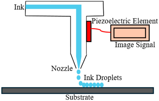
Figure 4.
An Inkjet Printing schematic demonstrating ink reservoir, piezoelectric element, nozzle and substrate interaction.
2.2.1. Advantages and Disadvantages
Inkjet printing is cost-effective, scalable, and compatible with high-throughput manufacturing. Its maskless nature allows rapid design changes through the simple modification of print files, making it ideal for prototyping and customized packaging solutions. Inkjet system support multilayer printing and enables the fabrication of redistribution layers, printed antennas, and embedded passive components. Short interconnects length achieved through inkjet printing reduce parasitic resistance and inductance, improving electrical performance in high-frequency packages [49,50,51].
Inkjet printing is highly sensitive to ink properties, requiring strict control of viscosity, surface tension, and particle size to prevent nozzle clogging. Maintenance procedures such as purging and cleaning increases material waste and downtime. Additionally, achieving ultra-fine resolution below a few micrometers remains challenging, and printed features may suffer from thickness nonuniformity and coffee-ring effects, which can degrade RF performance [52].
2.2.2. Relevance to Electronic Integration and Packaging
Inkjet Printing is widely used in electronic packaging for printed interconnects, redistribution layers, antennas, and multilayer RF structures. When combined with other additive manufacturing techniques, it enables hybrid packaging platforms that integrate electrical functionality directly into structural components [53,54,55,56].
2.3. Vat Polymerization
Vat polymerization is a class of additive manufacturing techniques in which liquid photopolymer resins are selectively cured using ultraviolet (UV) or visible light to form solid three-dimensional structures in a layer-by-layer manner. The process begins with a computer-aided design (CAD) model that is digitally sliced into thin two-dimensional layers. Each layer is sequentially exposed to patterned light, inducing photopolymerization and solidification of the resin [57]. Vat polymerization systems are commonly categorized into scanning-based stereolithography (SLA) [58] and projection-based digital light processing (DLP) (shown in Figure 5) [59]. In scanning-based systems, a focused laser beam traces the cross-section of each layer, curing the resin locally. In projection-based systems, an entire layer is cured simultaneously using a digital micromirror device (DMD) that projects a patterned light image onto the resin surface. Additionally, the platform systems comprise two main components: the building platform, where the part is constructed, and the elevator, responsible for raising and lowering the building platform. The vat’s liquid photocurable resin serves as the starting material. It is typically equipped with a level adjustment tool and an automated refilling pump. Gravity alone is unable to cause the resin surface to become flat because liquid resins used in vat polymerization have the potential to be rather viscous. Therefore, the resin is usually distributed, and its surface is uniformly flattened using a recoater blade. Furthermore, because projection-based printing system print each layer in a single pass, it takes less time to print. The scanning-based polymerization method, in contrast, cures each layer using a laser scanner. Large-scale printing can generally be done with SLA, but at the expense of resolution platforms, optics, and control systems. After each layer is cured, the build platform moves incrementally to allow fresh resin to coat the surface before the next exposure [60,61,62].
Figure 5.
A schematic illustration of vat polymerization processes: (left) scanning-based stereolithography (SLA); (right) projection-based digital light processing (DLP).
2.3.1. Advantages and Disadvantages
Vat polymerization offers exceptionally high dimensional accuracy and smooth surface finish, often reaching sub-micron roughness levels. This surface quality is particularly beneficial for electronic packaging, where smooth dielectric surfaces are required to minimize conductor roughness-induced losses at high frequencies. The ability to fabricate complex three-dimensional geometries with internal cavities and fine features enables the creation of advanced packaging structures such as air-filled substrates, waveguides and mechanically integrated housings. Projection-based systems further provide high throughput, making vat polymerization attractive for rapid fabrication of intricate dielectric components [63].
The primary limitation of vat polymerization lies in material availability. Most commercially available photopolymer resins exhibit limited thermal stability, mechanical strength, and dielectric performance compared to traditional PCB materials such as FR4 or ceramics. Moreover, post-processing steps including resin removal, cleaning, and UV post-curing add time and complexity to fabrication. Additionally, conventional vat polymerization does not inherently produce metallic conductive features, or conductive structures which can be realized using functionalized resins, such as MWCNT-filled photopolymers or intrinsically conductive polymer formulations. However, hybrid integration with direct-write techniques remains advantageous for achieving higher conductivity and multimaterial electronic packaging [64,65,66].
2.3.2. Relevance to Electronic Integration and Packaging
Vat polymerization plays a critical role in electronic packaging as a structural and dielectric fabrication platform. When combined with inkjet or aerosol jet printing, it enables fully additive manufactured structural electronics, including integrated antennas, RF substrates, and multi-functional package housings. Its high resolution and surface quality make it particularly suitable for mm-wave and RF packaging applications [67,68,69].
2.4. Extrusion Based Printing
2.4.1. Fused Filament Fabrication (FFF)
Fused filament fabrication (FFF), also called fused deposition modeling (FDM), is an extrusion-based additive manufacturing process in which thermoplastic filament is heated above its glass transition or melting temperature and extruded through a nozzle onto a build platform [70]. As shown in Figure 6, the filament is stored in a roller and directly linked to the extrusion head, which moves along the X and Y directions, while the build platform moves in the Z direction. Typically, two types of material filaments are used: supporting material and built material. While most FFF systems offer resolutions ranging from approximately 10 to 100 µm for the thickness of individual printed layers, the minimal XY feature dimension is constrained by the nozzle diameter, typically falling between 200 and 400 µm in nozzle systems. Some systems allow for the simultaneous deposition of multiple materials using additional nozzles. So, the FFF process typically consists of three stages: pre-processing, production, and post-processing. In the pre-processing stage, the product design is created using CAD (SolidWorks 2023/2024 or fusion 360) software, and crucial process parameters such as building orientation, machine temperature, and slicing parameters are determined. These parameters significantly influence the mechanical characteristics of the final product. As the extruded filament cools, it solidifies and bonds to previously deposited layers, gradually forming a three-dimensional object. Post-processing involves removing the product from the build platform, removing any supporting structures, and undergoing additional surface treatments to improve the product’s surface quality [29,70,71].
Figure 6.
Conceptual representation of fused filament fabrication (FFF), where material is deposited layer by layer to build a 3D object.
2.4.1.1. Advantages and Disadvantages
FFF is one of the most accessible and cost-effective additive manufacturing technologies, offering a wide selection of thermoplastic materials with diverse mechanical, thermal, and electrical properties. Multi-material printing enables the fabrication of structural components alongside insulating or thermally conductive materials. The robustness and simplicity of FFF systems make them suitable for rapid prototyping of electronic enclosures, fixtures, and low-cost packaging substrates [72,73,74].
FFF is limited by relatively low resolution, as the minimum feature size is constrained by nozzle diameter and extrusion dynamics. Printed parts typically exhibit high surface roughness and anisotropic mechanical properties due to interlayer bonding, which can negatively affect high-frequency electrical performance. Post-processing is often required to improve surface quality, increasing fabrication time [75,76].
2.4.1.2. Relevance to Electronic Integration and Packaging
In electronic packaging, FFF is primarily used for structural components, such as package housings, fixtures, and low-frequency substrates. While it is not ideal for fine-pitch interconnects or high-frequency circuits, FFF becomes valuable when integrated into hybrid manufacturing workflows, where conductive features are printed using inkjet or aerosol jet techniques onto FFF-fabricated structures [77,78,79,80].
2.4.2. Fluid Dispensing Based Printing
nScrypt printing is a precision micro-dispensing-based additive manufacturing technology that employs a patented SmartPump valve system to control material flow at the picolitre scale. Unlike conventional extrusion methods, the nScrypt system uses an actively actuated valve positioned near the dispensing orifice, allowing precise start-stop control of material deposition [31]. The schematic of nScrypt is shown in Figure 7, where the cross-sectional view of the valve assembly depicts a valve rod driven by a motor, traveling with a resolution of 0.1 µm within the valve body channel. The patented pen tip shape minimizes pressure requirements for material dispensing through very small holes, such as 100 microns or less. This assembly can handle highly viscous materials and loaded particles. Material is delivered from a syringe or cartridge under positive pressure into the valve chamber. When the valve opens, material is dispensed through a fine nozzle onto the substrate. Closing the valve induces a slight reverse flow, preventing droplet formation and stringing. This system enables high-speed printing with exceptional positional accuracy in the X, Y, and Z directions. Printing patterns can be generated by CAD software and transferred into script files using nScrypt software called nStudio (version 2021). Higher speeds enable rapid manufacturing, reducing costs, and maintenance [32,81,82].
Figure 7.
Working principle of nScrypt printing.
2.4.2.1. Advantages and Disadvantages
nScrypt printing supports a wide range of highly viscous and particle-loaded materials, including conductive pastes, dielectric polymers, and solder inks. The high level of flow control enables the fabrication of fine interconnects, and three-dimensional features with minimal material waste. The ability to print in true three dimensions makes nScrypt particularly suitable for advanced packaging applications [83,84].
Despite its precision, nScrypt printing systems are relatively expensive and less widely adopted compared to inkjet or FFF technologies. Build volumes are limited, and system complexity can increase maintenance requirements. Market adoption is still emerging, which limits standardized workflows [85,86].
2.4.2.2. Relevance to Electronic Integration and Packaging
nScrypt printing is extensively used in microelectronics packaging, including via filling, solder dispensing, printed interconnects, embedded components, and heterogeneous integration. Its capability to print fine features in three dimensions makes it a powerful tool for next-generation electronic packaging [87,88,89].
2.5. Comparison of Additive Manufacturing (AM) Techniques
Additive manufacturing and printed electronics techniques differ significantly in resolution, material compatibility, system cost and suitability for electronic integration and packaging. Aerosol jet printing (AJP) is particularly well-suited for high-resolution conductive interconnects, conformal circuits, and fine-feature electronic integration on complex or curved substrates, making it valuable for advanced packaging and embedded electronics. Inkjet Printing (IJP) enables scalable, cost-effective 2D deposition of functional materials and is widely used for printed circuit patterning and flexible electronics. Vat Polymerization (SLA/DLP) provides high structural accuracy and smooth surface finish, making it ideal for microfluidic devices, precision housings, and packaging components requiring tight tolerances. Fused Filament Fabrication (FFF) is best suited for low-cost structural prototyping and fabrication of mechanical enclosures or support structures for electronic assemblies. nScrypt printing enables true hybrid manufacturing by combining conductive, dielectric, and structural materials within a single platform, supporting integrated electronic packaging, embedded systems, and multifunctional device fabrication. The distinguishing technical capabilities and limitations of these processes are systematically summarized in Table 1 to highlight their suitability for structural fabrication, printed electronics, and integrated packaging applications.

Table 1.
Comparative table of additive and printed manufacturing techniques.
3. Example Applications of AM Technologies
While all five additive manufacturing techniques have merits for general prototyping and structural fabrication, where aerosol jet printing (AJP), inkjet printing (IJP), and nScrypt printing enable the precise deposition of conductive, dielectric, and structural materials on complex geometries, supporting embedded electronics, conformal traces, and multi-material integration. However, techniques such as fused filament fabrication (FFF) and vat polymerization (SLA/DLP) are generally less suitable for direct electronic integration and advanced packaging applications. FFF is primarily limited by its relatively coarse lateral resolution, large layer thickness, and difficulty in depositing conductive or functional inks, which restricts its ability to create fine interconnects or embedded circuitry. Similarly, vat polymerization achieves high structural precision but is constrained to photocurable resins and lacks compatibility with conductive and dielectric materials in multi-material architectures. Moreover, they are primarily used for substrate fabrication. Therefore, the following discussion of electronic integration and packaging focuses more on aerosol jet printing, inkjet printing and nScrypt printing, which can practically realize functional, multi-material devices and assemblies.
3.1. Printed Signal Crossovers Using Additive Manufacturing
Printed circuit boards (PCBs) are essential for connecting and supporting electronics components in a wide range of electronic devices [124]. In various electronic applications, including radar systems, communication transmitters, and optical drives, both radio frequency (RF) circuits and direct current (DC) circuits are commonly used [125,126]. Printed signal crossovers are critical building blocks in high-density electronic packaging, allowing multiple electrical signals to intersect without electrical shorting while maintaining signal integrity. Signal crossover may be necessary for integrating RF/DC, DC/DC or RF/RF electronics at the broad level to achieve effective packaging. When dealing with RF/DC signal lines, it’s crucial that the crossover maintains high isolation, low insertion loss, high DC carrying capacity, and high RF power handling capability. RF-DC crossovers are often solved with surface mount technology (SMT) components or multilayers designs in order to achieve these characteristics. SMT components for RF over RF are often not feasible due to limited isolation. To have a wide DC trace with high current capability, a large-sized chip is necessary. These components are limited in frequency ranges, sizes of signal traces, and power handling capabilities. Often, it is required to redesign the electronic schematic to fit in these bulky and rigid components [127]. Aerosol Jet Printing is a technology capable of depositing a variety of materials, including dielectric and conductive materials, on the microscale. This printing technique allows for precise deposition of dielectric material exclusively over the RF-DC crossover location, and subsequent deposition of conductive material over the dielectric can establish a connection to the top signal trace.
L. Clark et al. [128] investigates a direct ink writing approach using aerosol jet printing (AJP) to fabricate signal crossover structures, where one electrical trace passes over another without direct electrical contact, which are commonly needed in compact electronic systems as shown in Figure 8. Normally, such crossovers on circuit boards require additional physical layers, adding cost and weight for which authors propose an additive manufacturing solution to reduce that complexity. The electrical performance of the printed crossovers is evaluated through high-frequency S-parameter measurements in the X-band, showing minimal signal degradation due to the crossover structures. In addition, thermal and power handling tests are conducted to assess crossover reliability under elevated temperatures and applied power. The results indicate that aerosol jet printed crossovers can sustain functional RF operation while maintaining acceptable thermal stability.
Figure 8.
Direct-write printed signal crossover showing ramp and crossover printed on top of RF line.
Another study done by S. Romaguera et al. [129] presents one of the earliest demonstrations of fully printed signal crossover structures using inkjet printing. The authors fabricate metal-insulator-metal (MIM) crossover architectures, (as shown in Figure 9, adapted from reference [129]) where a printed dielectric layer electrically isolates two intersecting conductive silver traces. The study focuses on process feasibility, material compatibility, and multilayer build-up using sequential deposition and curing steps. This study establishes a fundamental manufacturing framework for additive signal crossovers and highlights key challenges such as layer uniformity and registration accuracy that remain relevant to modern aerosol jet and direct-write crossover fabrication techniques.
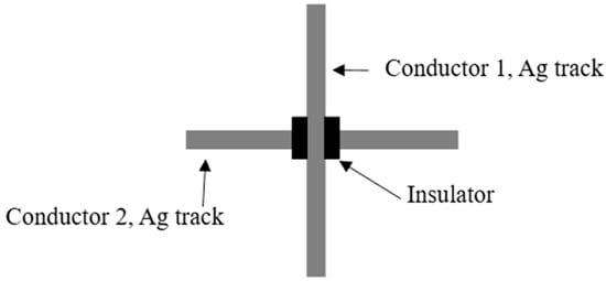
Figure 9.
Schematic of metal–insulator–metal (MIM) crossover illustrating two conductive layers separated by an insulator for signal routing.
Recent research has addressed the persistent challenge of signal crossovers in compact circuit designs through innovative placement and routing strategies. In the context of inkjet-printed electronics, crossover-aware placement and routing has been proposed by F. Rasheed [130] to minimize overlapping conductive traces, enhancing reliability and print yield on flexible substrates without increasing design complexity as shown in Figure 10 (adapted from reference [130]). Complementing this approach, a novel surface-mount method by A. Microwave Inc. [131] demonstrates crossover signals in conventional SMT circuits without adding extra PCB layers, maintaining signal integrity while simplifying manufacturing. Together, these studies highlight a broader trend in circuit design, developing efficient techniques to manage crossovers across both flexible and traditional electronics. Challenges such as dielectric loss, alignment accuracy, and reliability are also addressed. Overall, printed crossovers are shown to be critical for compact and high-density RF integration.
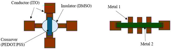
Figure 10.
Diagram of a printed crossover structure (left) featuring indium tin oxide (ITO) conductors insulated by dimethyl sulfoxide (DMSO), with a PEDOT: PSS crossover region and (right) illustrates stacked Metal 1 and Metal 2 layers providing electrical separation for signal routing in additive electronics.
Laser-enhanced direct print additive manufacturing (LE-DPAM) is an additive manufacturing technique that combines aerosol jet printing of metallic nanoparticle inks with localized laser sintering. In this process, metallic ink is deposited in a controlled manner while a focused laser beam simultaneously sinters the material, enabling rapid solidification and mechanical stability during printing. A key advantage of LE-DPAM is its ability to fabricate self-supporting 3D structures such as vertical posts, bridges, interconnects and crossovers, directly on planar substrates.
Firat et al. [132] demonstrated a low-loss suspended crossover interconnect fabricated using LE-DPAM. Conventional planar crossover interconnects suffer from increased dielectric loss and parasitic capacitance due to close proximity to the substrate, particularly at microwave frequencies. The proposed suspended architecture addresses these limitations by elevating the crossover conductor above the substrate, allowing the electromagnetic fields to propagate primarily through air. As illustrated in Figure 11 (adapted from reference [132]), the fabrication process begins with printing the bottom transmission line, followed by vertical metallic support posts formed using simultaneous aerosol jet deposition and laser sintering. A horizontal metallic bridge is then printed across the posts to form a crossover without the need for a sacrificial layer or multilayer dielectrics. Experimental S-parameter measurements show improved insertion loss and reduced signal degradation compared to conventional planar crossovers. These additive manufacturing approaches offer a simple, low-cost, and flexible method for fabricating three-dimensional crossovers, making them suitable for microwave packaging, and heterogeneous electronic integration.
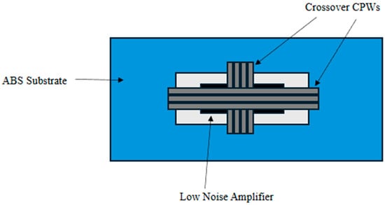
Figure 11.
Schematic layout of crossover coplanar waveguides (CPWs) integrated on an ABS substrate, featuring crossover CPWs and a low noise amplifier for signal processing.
3.2. Printed 3D Interconnects and Ramps for Packaging Topologies
For optimal packages, careful consideration is required for interconnect size, parasitic effects, coefficient or thermal expansion, and potential detuning caused by molding or nearby components. Addressing these concerns involves implementing a novel packaging solution utilizing printed fully 3D interconnects, capitalizing on the advantage offered by high-resolution additive manufacturing. In the past, the electronics industry has heavily relied on wire and ribbon bonding, as well as printing interconnects, to establish dependable connections. However, advancements in electronic production have necessitated the development of better, more reliable interconnects scalable for high-volume manufacturing. Annually, this industry generates over ten trillion semiconductor interconnects, amounting to thousands per person globally. While wire bonding has been the primary method for the past 50 years, it is not without its drawbacks. Failures can occur due to contamination, unstable substrate surfaces, sequential interconnection processes, and metallurgical issues, leading to significant cost. To address these challenges, AM ramp interconnects are being adopted to replace bond wires in mm-wave RF packages. The fabrication of flexible 3D structures can be challenging due to thick underlying material layers acting as support structures, causing deformation during subsequent 3D printing processes. However, combining flexible 3D printing and inkjet deposition enables the creation of heterogeneous packages using nonpolar interconnects across ICs of varying heights, enhancing performance [71,133,134].
Three-dimensional interconnects and ramp-based transitions (shown in Figure 12) represent one of the most impactful applications of additive manufacturing in electronic integration, particularly as alternatives to conventional wire bonding. These are essential for modern electronic packages, where multiple dies and components must be interconnected across varying height levels. Partially, SLA-printed high-speed interconnects have demonstrated the creation of a new low-crosstalk structure capable of achieving high-density interconnects. Moreover, extensive research has also demonstrated that inkjet and aerosol jet printed ramp structures support high-frequency operations up to tens of gigahertz, making them suitable for mm-wave and RF-packaging. These interconnects can be fabricated post-assembly, enabling repair, customization, and design iteration. Integration of ramp interconnects with 3D printed dielectric substrates has further enabled a fully additive manufacturing packaging platform incorporating antennas, transmission lines, and embedded passives. Also, ramp-based packaging topologies are increasingly important for heterogeneous integration, where chips of varying sizes, materials, and heights must be interconnected within a single package [135,136,137,138].
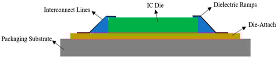
Figure 12.
Schematic cross-sectional illustration of 3D-printed interconnects and ramps.
The introduction of a novel “ramp” interconnect structure in 2016, utilizing inkjet printing technologies, further demonstrated practical packaging topologies. Integrating 3D printing with inkjet printing allows for the post-process fabrication of on-package components, antennas, and meta-material structures. As three-dimensional first level interconnections become essential for establishing communication between IC dies, packaging substrates, and other electronic elements within the same package, wire bonding and flip-chip techniques are the prevailing methodologies. While wire bonding offers an economical approach, it is susceptible to displacement during molding and induces substantial parasitic inductance, often requiring passive component incorporation to offset these effects. On the other hand, flip-chip techniques curtail interconnection length and parasitic effects, although they are vulnerable to mismatches in the coefficient of thermal expansion and can experience frequency detuning due to their proximity to on-package signal pathways below the IC. So, to evaluate these existing hurdles related to cost and adaptability in wireless system-on-package solutions, this technique of 3D interconnects and ramps is a swift, entirely additive electronic manufacturing method that offers advantages such as minimal material wastage, lowered expenses, and increased design adaptability [139,140,141].
Recent studies have been done by two different groups of authors; first, Feng et al., [142] examine the use of aerosol jet printing (AJP) to fabricate conformal interconnects for millimeter-wave RF systems as an alternative to traditional interconnect techniques like wire bonding and microstrip lines in 2023. The authors show that AJP can digitally design and deposit conductive silver nanoparticle interconnects (as shown in Figure 13 (left)) directly onto 3D surfaces of RF packages, significantly reducing parasitic inductance and signal loss at high frequencies up to 110 GHz. And the second group of authors, Kexin et al., [143] demonstrate fully inkjet-printed 3D ramp interconnects optimized for flexible and conformal electronics in the 5G/mm-wave frequency bands (20–40 GHz) in 2024. The authors fabricate multilayer SU-8 dielectric ramps and printed silver nanoparticle conductive traces that bridge microstrip lines to attached die pads. (shown in Figure 13 (right) adapted from reference [143]) This work extends earlier rigid-substrate ramp designs into flexible heterogeneous systems, establishing additive printed ramp interconnects as viable for integrated 5G/mm wave conformal devices. Both studies underscore the importance of geometry-controlled, direct-write interconnects in advancing next-generation electronic packaging and multilayer printed electronic architectures.
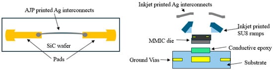
Figure 13.
(left) Diagram shows Ag interconnects printed by AJP on a SiC wafer. (right) Demonstration of flexible inkjet-printed 3D “ramp” interconnects.
3.3. Advanced Packaging Approach for Enhancing Performance
Additive manufacturing has become a key technology for advanced electronic packaging and high-frequency devices due to its ability to fabricate complex structures with high precision. The electronics industry consistently demands more functionality, faster speeds, and lower power consumption. Significant efforts have been devoted to advancing high-density electronic packaging and integration in recent years, encompassing various initiatives such as PCB-embedded designs, 3D chip stacking, metal-embedded chip assembly (MECA), multi-chip modules (MCMs), monolithic microwave integrated circuit (MMIC) and heterogenous integration [18,144,145]. In PCB-embedded designs, interconnections to embedded devices are shortened, minimizing parasitic inductances, as well as reducing system volume and weight. A common approach to PCB-embedded technology involves vertically stacking layers of PCBs and prepreg layers, creating cavities in between to host embedded devices. However, this method, while widely used, is susceptible to errors. The alignment of cavities during stacking and variations in thermal expansion coefficients during thermal curing can lead to issues. Additionally, precise alignment of vias to access embedded devices, especially in bare die form, presents challenges [146]. To address these complications, an alternative technique for embedding devices into PCBs is employed. This method involves embedding devices in a high thermal conductivity metallic matrix inside the PCB, utilizing a combination of subtractive and additive manufacturing technologies. Unlike traditional methods, this approach requires only a single PCB layer, eliminating the need for drilling and plating of vias to connect to embedded devices [147,148,149].
Aga et al. [150] introduce an additive manufacturing-based strategy for embedding semiconductor chips within a metallic matrix-infused printed circuit board (PCB) as shown in Figure 14 (adapted from reference [150]) to improve integration and performance of electronic systems. The process leverages additive deposition and metallic matrix infusion techniques to directly incorporate bare chips into the circuit board substrate, creating a monolithic composite structure rather than mounting a discrete package onto a standard PCB. The proposed method aims to enhance electrical interconnection density, thermal management, and mechanical robustness by embedding chips in a conductive metallic matrix that surrounds and supports the devices. This architecture potentially reduces parasitic effects and improves heat dissipation compared with traditional surface mounting and soldering approaches used in conventional PCB assembly. The work contributes to emerging research on chip-embedding and heterogeneous integration, where additive processes are explored to push beyond the limits of conventional PCB fabrication and assembly.
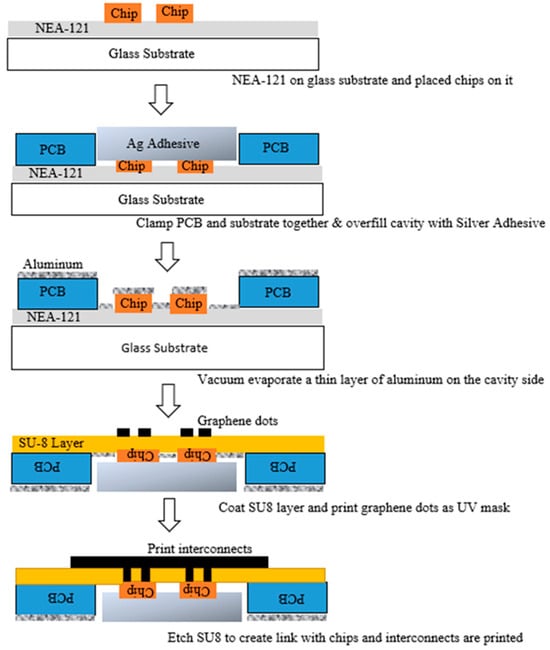
Figure 14.
Process flow of chips embedded in metallic matrix inside a PCB using additive manufacturing (AM) technology.
The continuous demand for high-performance RF systems has driven research into innovative chip integration and packaging strategies. Conventional wire-bond and flip-chip approaches often suffer from parasitic losses, limited thermal management, and impedance mismatches, which constrain circuit performance at high frequencies. To address these challenges, Estrada et al. [151] introduced a Metal-Embedded Chip Assembly (MECA) process, in which active RF chips and passive components are embedded into a metallic ground structure as shown in Figure 15 (adapted from reference [151]). This approach simultaneously improves electrical interconnect quality, thermal dissipation, and design flexibility, providing a foundation for enhanced RF circuit performance.
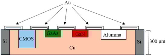
Figure 15.
Schematic of a MECA process cross-sectional shows that RF chips and passive components are embedded within a Si interposer wafer.
Photolithographically defined bridge transmission lines are used as interconnects, replacing wire bonds, and enabling precise impedance control with significantly reduced parasitic inductance and loss. Experimental results demonstrate that MECA interconnects provide superior RF performance over a wide frequency range, with improved characteristic impedance and lower insertion loss compared to traditional microstrip and wire-bond transitions. The authors further validate the technique through the integration of passive RF components and a GaN power amplifier, showing measurable improvements in gain and power-added efficiency. Overall, the additive and MECA process represents a promising heterogeneous integration strategy for high-frequency and high-power RF systems, offering enhanced electrical performance, improved thermal management, and increased design flexibility [152,153].
AM has emerged as a versatile approach for advanced electronic packaging and RF systems. Z. Shen et al. [154] investigated additive manufacturing approaches for multi-chip modules (MCMs), demonstrating how these techniques can enable precise interconnects, compact layouts, and improved module integration, which are critical for high-density electronics. Figure 16 shows the cross section of AM-MCM where interconnects (black), components (red, yellow, green, orange) and insulations (blue) are deposited. Another study done by A. Obeidat et al. [155] focused on additive electronics for embedded RF die packaging and multi-chip phased array modules, showing that additive approaches can simplify assembly processes, enhance design flexibility, and support scalable integration of multiple components in a single module. Furthermore, A. Mohamed [142] discussed that laser-enhanced direct-print additive manufacturing has been applied to W-band monolithic microwave integrated circuit (MMIC) chip assembly, achieving highly accurate placement and excellent RF performance at millimeter-wave frequencies, which is essential for next generation high-frequency communication systems. Together, these works highlight how additive manufacturing is transforming the design and assembly of multi-chip and high-frequency electronic systems by enabling compact, high-performance, and scalable solutions.
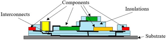
Figure 16.
Schematic cross-sectional illustration of additive manufacturing (AM) multi-chip module (MCM), showing integrated components, interconnect structure, and insulating layers assembled on a substrate.
Moreover, embedded packaging architecture provides a foundation for three-dimensional stacked integration, resulting in enhanced electrical performance and improved thermal management [156,157]. Studies on advanced packaging approaches for power electronics, such as 3-D dimensional integration, press-fit packaging, and hybrid packaging schemes can be broadly categorized with the domain of embedded packaging technologies [158,159,160].
4. Future of AM in Electronic Assembly and Manufacturing
Additive manufacturing (AM) is expected to play an increasingly critical role in the future of electronic assembly and manufacturing as the demand for higher integration density, improved electronic performance, and customized packaging architectures continues to grow. While current AM techniques have demonstrated significant potential for prototyping and small-scale production, their long-term impact will be defined by advances in materials, process integration, scalability, and reliability [161,162,163,164].
- (a)
- Advances in Materials: Research into advanced conductive inks, dielectric materials, and hybrid composites will expand the capabilities of AM for electronics, enabling higher performance and better reliability for components like flexible circuits and embedded systems. Such capabilities would enable the fabrication of fully integrated electronic packages in a single manufacturing flow, eliminating the need for multiple fabrication, assembly, and alignment steps common in conventional packaging.
- (b)
- Custom and On-demand Manufacturing: The ability to produce electronic components on-demand allows manufacturers to quickly prototype and customize products, significantly shortening development cycles and reducing inventory requirements.
- (c)
- Enhanced Design Freedom: AM allows for the creation of complex geometries and custom designs that are difficult or impossible to achieve with traditional manufacturing techniques. This opens the door to innovative electronic components, including lightweight and compact devices.
- (d)
- Integration of Multifunctionality: AM enables the integration of diverse functionalities such as sensors, antennas, and circuits which are embedded directly into structures or devices. This minimizes assembly steps and enhances system performance.
- (e)
- Sustainability and Cost-Effectiveness: By reducing material waste, energy consumption, and production steps, AM offers a more sustainable and cost-efficient alternative to traditional manufacturing. The use of recyclable and bio-based materials in AM could further enhance its eco-friendly potential.
- (f)
- Smart Packaging Solutions: The development of additive-based smart packaging, such as ramp topologies and embedded interconnects, will further enhance the reliability and functionality of electronic devices, especially in high-frequency applications.
5. Summary
This paper has reviewed various additive manufacturing (AM) technologies from the perspective of electronic integration and packaging. By systematically examining aerosol jet printing, inkjet printing, vat polymerization, fused filament fabrication, and fluid-dispensing-based nScrypt printing, this work highlights how each technique offers unique capabilities and limitations in terms of resolution, material compatibility, scalability, and reliability. Collectively, these technologies provide unprecedented design freedom and enable advanced packaging architectures that are difficult or impossible to realize using conventional subtractive manufacturing approaches. Applications such as printed signal crossovers, three-dimensional interconnects, ramp-based transitions, and embedded chip assemblies demonstrate the potential of additive manufacturing to enhance integration density and support high-frequency operation. Furthermore, the future of AM in electronic assembly and manufacturing is discussed. Ultimately, additive manufacturing is poised to become a key enabling technology for next-generation electronic packaging, supporting the development of compact, high-performance, and applications in specific electronic systems.
Author Contributions
Conceptualization, A.S., A.M.; methodology, A.S., A.M.; formal analysis, A.S., A.M.; investigation, A.S., A.M.; resources, A.M.; data curation, A.S.; writing—original draft preparation, A.S.; writing—review and editing, A.S., A.M.; visualization, A.S.; supervision, A.M.; project administration, A.M. All authors have read and agreed to the published version of the manuscript.
Funding
The research received no external funding.
Data Availability Statement
This review is based on previously published studies and publicly available data. All relevant data are cited within the article.
Conflicts of Interest
The authors declare no conflict of interest.
References
- Chen, J.; Yuan, Y.; Wang, Q.; Wang, H.; Advincula, R.C. Bridging Additive Manufacturing and Electronics Printing in the Age of AI. Nanomaterials 2025, 15, 843. [Google Scholar] [CrossRef]
- Wilkinson, N.J.; Smith, M.A.A.; Kay, R.W.; Harris, R.A. A review of aerosol jet printing—A non-traditional hybrid process for micro-manufacturing. Int. J. Adv. Manuf. Technol. 2019, 105, 4599–4619. [Google Scholar] [CrossRef]
- Stringer, J.; Althagathi, T.M.; Tse, C.C.W.; Ta, V.D.; Shephard, J.D.; Esenturk, E.; Connaughton, C.; Wasley, T.J.; Li, J.; Kay, R.W.; et al. Integration of additive manufacturing and inkjet printed electronics: A potential route to parts with embedded multifunctionality. Manuf. Rev. 2016, 3, 12. [Google Scholar] [CrossRef]
- Bailey, C.; Stoyanov, S.; Tilford, T.; Tourloukis, G. 3D-Printing and Electronic Packaging. In 2016 Pan Pacific Microelectronics Symposium (Pan Pacific); IEEE: New York, NY, USA, 2016. [Google Scholar]
- Zhou, H.; Zhang, Y.; Cao, J.; Su, C.; Li, C.; Chang, A.; An, B. Research Progress on Bonding Wire for Microelectronic Packaging. Micromachines 2023, 14, 432. [Google Scholar] [CrossRef] [PubMed]
- Pascariu, G.; Cronin, P.; Mrsi, D.C. Next Generation Electronics Packaging Utilizing Flip Chip Technology. In IEEE/CPMT/SEMI 28th International Electronics Manufacturing Technology Symposium, 2003. IEMT 2003; IEEE: New York, NY, USA, 2003. [Google Scholar]
- Kwon, D.H.; Kim, J.; Kim, K.H.; Choi, S.C.; Lim, J.H.; Park, J.H.; Choi, L.; Hwang, S.W.; Lee, S.H. Characterization and modeling of a new via structure in multilayered printed circuit boards. IEEE Trans. Compon. Packag. Technol. 2003, 26, 483–489. [Google Scholar] [CrossRef]
- John, W. The Effects of Package Parasitic on the Stability of Microwave Negative Resistance Devices. IEEE Trans. Microw. Theory Tech. 1973, 21, 731–735. [Google Scholar] [CrossRef]
- Betancur-Muñoz, P.; Osorio-Gómeza, G.; Martínez-Cadavid, J.F.; Duque-Lombana, J.F. Integrating design for assembly guidelines in packaging design with a context-based approach. Procedia CIRP 2014, 21, 342–347. [Google Scholar] [CrossRef][Green Version]
- Chen, W.T.; Trivedi, A.K.; Welsh, J.A. Manufacturing challenges in electronic packaging: An overview. In Manufacturing Challenges in Electronic Packaging; Springer: Boston, MA, USA, 1998. [Google Scholar]
- Ghazali, M.I.M.; Karuppuswami, S.; Kaur, A.; Chahal, P. 3D Printed Air Substrates for the Design and Fabrication of RF Components. IEEE Trans. Compon. Packag. Manuf. Technol. 2017, 7, 982–989. [Google Scholar] [CrossRef]
- Ray, U.; Cho, N.J.; Kim, Y.C.; Yoon, S.W.; Choi, W.K.; Marimuthu, P. Packaging and Integration Strategy for mm-Wave Products. Int. Symp. Microelectron. 2018, 2018, 000252–000258. [Google Scholar] [CrossRef]
- Ali, M.; Watanabe, A.; Kakutani, T.; Raj, P.M.; Tummala, R.R.; Swaminathan, M. Package Integration and System Performance Analysis of Glass-Based Passive Components for 5G New Radio Millimeter-Wave Modules. Electronics 2025, 14, 1670. [Google Scholar] [CrossRef]
- Tehrani, B.K.; Bahr, R.A.; Tentzeris, M.M. Inkjet and 3D printing technology for fundamental millimeter-wave wireless packaging. J. Microelectron. Electron. Packag. 2018, 15, 101–106. [Google Scholar] [CrossRef]
- Zhou, Z.; Li, Z.; Zhang, W.; Bian, Y.; Qiu, X.; Huang, L.; Chen, M. Micro-nano additive manufacturing for advanced electronic packaging of singulated chips. Mater. Today Electron. 2025, 13, 100168. [Google Scholar] [CrossRef]
- Knausenberger, W. Electronic Packaging Design: Fundamentals. In Encyclopedia of Materials: Science and Technology; Buschow, K.H.J., Cahn, R.W., Flemings, M.C., Ilschner, B., Kramer, E.J., Mahajan, S., Veyssière, P., Eds.; Elsevier: Oxford, UK, 2001; pp. 2659–2666. [Google Scholar] [CrossRef]
- Tummala, R.R. Packaging: Past, Present and Future. In 2005 6th International Conference on Electronic Packaging Technology; IEEE: New York, NY, USA, 2006. [Google Scholar]
- Ulrich, R.K.; Brown, W.D. Advanced Electronic Packaging; John Wiley & Sons: Hoboken, NJ, USA, 2006. [Google Scholar]
- Shahrubudin, N.; Lee, T.C.; Ramlan, R. An overview on 3D printing technology: Technological, materials, and applications. Procedia Manuf. 2019, 35, 1286–1296. [Google Scholar] [CrossRef]
- Jiménez, M.; Romero, L.; Domínguez, I.A.; Espinosa, M.D.M.; Domínguez, M. Additive Manufacturing Technologies: An Overview about 3D Printing Methods and Future Prospects. Complexity 2019, 2019, 1–30. [Google Scholar] [CrossRef]
- Praveena, B.A.; Lokesh, N.; Buradi, A.; Santhosh, N.; Praveena, B.L.; Vignesh, R. A comprehensive review of emerging additive manufacturing (3D printing technology): Methods, materials, applications, challenges, trends and future potential. Mater. Today Proc. 2022, 52, 1309–1313. [Google Scholar] [CrossRef]
- Gibson, I.; Rosen, D.; Stucker, B.; Khorasani, M. Additive Manufacturing Technologies; Springer: Cham, Switzerland, 2021. [Google Scholar]
- Calignano, F.; Manfredi, D.; Ambrosio, E.P.; Biamino, S.; Lombardi, M.; Atzeni, E.; Salmi, A.; Minetola, P.; Iuliano, L.; Fino, P. Overview on additive manufacturing technologies. Proc. IEEE 2017, 105, 593–612. [Google Scholar] [CrossRef]
- Secor, E.B. Principles of aerosol jet printing. Flex. Print. Electron. 2018, 3, 035002. [Google Scholar] [CrossRef]
- Singh, M.; Haverinen, H.M.; Dhagat, P.; Jabbour, G.E. Inkjet printing-process and its applications. Adv. Mater. 2010, 22, 673–685. [Google Scholar] [CrossRef] [PubMed]
- Calvert, P. Inkjet printing for materials and devices. Chem. Mater. 2001, 13, 3299–3305. [Google Scholar] [CrossRef]
- Sampson, K.L.; Deore, B.; Go, A.; Nayak, M.A.; Orth, A.; Gallerneault, M.; Malenfant, P.R.L.; Paquet, C. Multimaterial Vat Polymerization Additive Manufacturing. ACS Appl. Polym. Mater. 2021, 3, 4304–4324. [Google Scholar] [CrossRef]
- Zhang, F.; Zhu, L.; Li, Z.; Wang, S.; Shi, J.; Tang, W.; Li, N.; Yang, J. The recent development of vat photopolymerization: A review. Addit. Manuf. 2021, 48, 102423. [Google Scholar] [CrossRef]
- Rajan, K.; Samykano, M.; Kadirgama, K.; Harun, W.S.W.; Rahman, M.M. Fused deposition modeling: Process, materials, parameters, properties, and applications. Int. J. Adv. Manuf. Technol. 2022, 120, 1531–1570. [Google Scholar] [CrossRef]
- Nassar, H.; Dahiya, R. Fused Deposition Modeling-Based 3D-Printed Electrical Interconnects and Circuits. Adv. Intell. Syst. 2021, 3, 2100102. [Google Scholar] [CrossRef]
- Chen, X.; Church, K. Direct Printing for Next Generation High Density Packaging. Int. Symp. Microelectron. 2011, 2011, 001007–001011. Available online: http://meridian.allenpress.com/ism/article-pdf/2011/1/001007/2343877/isom-2011-tha4-paper1.pdf (accessed on 3 December 2025).
- Oh, D.; Kim, N. High Viscose Ink Jetting by using nScrypt Head and Application. In Proceedings of the IEEE International Symposium on Assembly and Manufacturing, Suwon, Republic of Korea, 17–20 November 2009. [Google Scholar]
- Craton, M.T.; Konstantinou, X.; Albrecht, J.D.; Chahal, P.; Papapolymerou, J. Additive Manufacturing of a W-Band System-on-Package. IEEE Trans. Microw. Theory Tech. 2021, 69, 4191–4198. [Google Scholar] [CrossRef]
- Miettinen, J.; Pekkanen, V.; Kaija, K.; Mansikkamäki, P.; Mäntysalo, J.; Mäntysalo, M.; Niittynen, J.; Pekkanen, J.; Saviauk, T.; Rönkkä, R. Inkjet printed System-in-Package design and manufacturing. Microelectron. J. 2008, 39, 1740–1750. [Google Scholar] [CrossRef]
- He, X.; Hu, K.; Cui, Y.; Bahr, R.; Tehrani, B.; Tentzeris, M.M. Additively Manufactured “Smart” RF/mm-Wave Packaging Structures: A Quantum Leap for On-Demand Customizable Integrated 5G and Internet of Things Modules. IEEE Microw. Mag. 2022, 23, 94–106. [Google Scholar] [CrossRef]
- Feng, J.Q.; Renn, M.J. Aerosol Jet® Direct-Write for Microscale Additive Manufacturing. J. Micro Nanomanuf. 2019, 7, 011004. [Google Scholar] [CrossRef]
- Jeong, H.; Lee, J.H.; Kim, S.; Han, S.; Moon, H.; Song, J.Y.; Park, A.Y. Optimization of process parameters in micro-scale pneumatic aerosol jet printing for high-yield precise electrodes. Sci. Rep. 2023, 13, 21297. [Google Scholar] [CrossRef] [PubMed]
- Gupta, A.A.; Bolduc, A.; Cloutier, S.G.; Izquierdo, R. Aerosol Jet Printing for printed electronics rapid prototyping. In 2016 IEEE International Symposium on Circuits and Systems (ISCAS); IEEE: New York, NY, USA, 2016; pp. 866–869. [Google Scholar] [CrossRef]
- Seiti, M.; Degryse, O.; Ferraro, R.M.; Giliani, S.; Bloemen, V.; Ferraris, E. 3D Aerosol Jet® printing for microstructuring: Advantages and Limitations. Int. J. Bioprint. 2023, 9, 57–74. [Google Scholar] [CrossRef]
- Binder, S.; Glatthaar, M.; Rädlein, E. Analytical investigation of aerosol jet printing. Aerosol Sci. Technol. 2014, 48, 924–929. [Google Scholar] [CrossRef]
- Seifert, T.; Baum, M.; Roscher, F.; Wiemer, M.; Gessner, T. Aerosol Jet Printing of Nano Particle Based Electrical Chip Interconnects. Mater. Today Proc. 2015, 2, 4262–4271. [Google Scholar] [CrossRef]
- Gupta, A.A.; Soer, M.C.M.; Taherzadeh-Sani, M.; Cloutier, S.G.; Izquierdo, R. Aerosol-jet printed transmission lines for microwave packaging applications. IEEE Trans. Compon. Packag. Manuf. Technol. 2019, 9, 2482–2489. [Google Scholar] [CrossRef]
- Christenson, K.K.; Paulsen, J.A.; Renn, M.J.; McDonald, K.; Bourassa, J.; Paul, S. Direct Printing of Circuit Boards Using Aerosol Jet®. Nip Digit. Fabr. Conf. 2011, 27, 433–436. [Google Scholar] [CrossRef] [PubMed]
- Spain, W.; Papapolymerou, J.; Chahal, P.; Hodek, M.; Albrecht, J.D. Aerosol-Jet Printed Transferable Millimeter-Wave Circuits. IEEE Trans. Compon. Packag. Manuf. Technol. 2024, 14, 1723–1730. [Google Scholar] [CrossRef]
- Jo, B.W.; Lee, A.; Ahn, K.H.; Lee, S.J. Evaluation of jet performance in drop-on-demand (DOD) inkjet printing. Korean J. Chem. Eng. 2009, 26, 339–348. [Google Scholar] [CrossRef]
- Singh, A.; Mian, A. Processing and Characterization of Functional Ink Materials for Flexible Hybrid Electronics. In 2025 1st International Conference on Secure IoT, Assured and Trusted Computing (SATC); Institute of Electrical and Electronics Engineers Inc.: Dayton, OH, USA, 2025. [Google Scholar] [CrossRef]
- Döring, M. Ink-jet printing. IEEE Trans. Electron Devices 1973, 20, 14–19. [Google Scholar]
- Cummins, G.; Desmulliez, M.P.Y. Inkjet printing of conductive materials: A review. Circuit World 2012, 38, 193–213. [Google Scholar] [CrossRef]
- Subramanian, V.; Chang, J.; de la Fuente Vornbrock, A.; Molesa, S.; Soltman, D.; Zhang, Q. Printed organic transistors for low-cost tagging and sensing applications. In Polytronic 2007—6th International Conference on Polymers and Adhesives in Microelectronics and Photonics; IEEE: New York, NY, USA, 2007; pp. 1–5. [Google Scholar] [CrossRef]
- Mengel, M.; Nikitin, I. Inkjet printed dielectrics for electronic packaging of chip embedding modules. Microelectron. Eng. 2010, 87, 593–596. [Google Scholar] [CrossRef]
- Søndergaard, R.R.; Hösel, M.; Krebs, F.C. Roll-to-Roll fabrication of large area functional organic materials. J. Polym. Sci. B Polym. Phys. 2013, 51, 16–34. [Google Scholar] [CrossRef]
- Castrejón-Pita, J.R.; Baxter, W.R.S.; Morgan, J.; Temple, S.; Martin, G.D.; Hutchings, I.M. Future, Opportunities and Challenges of Inkjet Technologies. At. Sprays 2013, 23, 541–565. [Google Scholar] [CrossRef]
- Perelaer, J.; Smith, P.J.; Mager, D.; Soltman, D.; Volkman, S.K.; Subramanian, V.; Korvink, J.G.; Schubert, U.S. Printed electronics: The challenges involved in printing devices, interconnects, and contacts based on inorganic materials. J. Mater. Chem. 2010, 20, 8446–8453. [Google Scholar] [CrossRef]
- Laurila, M.-M. Mika-Matti Laurila Super Inkjet Printed Redistribution Layer for a Mems Device. Master’s Thesis, Tampere University of Technology, Tampere, Finland, 2015. [Google Scholar]
- Cook, B.S.; Shamim, A. Inkjet printing of novel wideband and high gain antennas on low-cost paper substrate. IEEE Trans. Antennas Propag. 2012, 60, 4148–4156. [Google Scholar] [CrossRef]
- Yang, L.; Rida, A.; Vyas, R.; Tentzeris, M.M. RFID tag and RF structures on a paper substrate using inkjet-printing technology. IEEE Trans. Microw. Theory Tech. 2007, 55, 2894–2901. [Google Scholar] [CrossRef]
- Marasso, S.L.; Cocuzza, M. High Resolution Manufacturing from 2D to 3D/4D Printing: Applications in Engineering and Medicine; Springer International Publishing: Berlin/Heidelberg, Germany, 2022. [Google Scholar] [CrossRef]
- Emami, M.M.; Barazandeh, F.; Yaghmaie, F. Scanning-projection based stereolithography: Method and structure. Sens. Actuators A Phys. 2014, 218, 116–124. [Google Scholar] [CrossRef]
- Guven, E.; Karpat, Y.; Cakmakci, M. Improving the dimensional accuracy of micro parts 3D printed with projection-based continuous vat photopolymerization using a model-based grayscale optimization method. Addit. Manuf. 2022, 57, 102954. [Google Scholar] [CrossRef]
- Çerlek, Ö.; Kesercioğlu, M.A.; Han, K. Stereolithography(SLA): An Innovative Additive Manufacturing Process. In New Trends and Frontiers in Engineering; All Sciences Academy: Konya, Turkey, 2024. [Google Scholar]
- Borrello, J.; Nasser, P.; Iatridis, J.C.; Costa, K.D. 3D printing a mechanically-tunable acrylate resin on a commercial DLP-SLA printer. Addit. Manuf. 2018, 23, 374–380. [Google Scholar] [CrossRef] [PubMed]
- Zakeri, S.; Vippola, M.; Levänen, E. A comprehensive review of the photopolymerization of ceramic resins used in stereolithography. Addit. Manuf. 2020, 35, 101177. [Google Scholar] [CrossRef]
- Colorado, H.A.; Gutierrez-Velasquez, E.I.; Gil, L.D.; de Camargo, I.L. Exploring the advantages and applications of nanocomposites produced via vat photopolymerization in additive manufacturing: A review. Adv. Compos. Hybrid Mater. 2024, 7, 1. [Google Scholar] [CrossRef]
- Sezer, H.K.; Eren, O. FDM 3D printing of MWCNT re-inforced ABS nano-composite parts with enhanced mechanical and electrical properties. J. Manuf. Process. 2019, 37, 339–347. [Google Scholar] [CrossRef]
- Ng, W.L.; Lee, J.M.; Zhou, M.; Chen, Y.W.; Lee, K.X.A.; Yeong, W.Y.; Shen, Y.F. Vat polymerization-based bioprinting—Process, materials, applications and regulatory challenges. Biofabrication 2020, 12, 022001. [Google Scholar] [CrossRef]
- Quan, H.; Zhang, T.; Xu, H.; Luo, S.; Nie, J.; Zhu, X. Photo-curing 3D printing technique and its challenges. Bioact. Mater. 2020, 5, 110–115. [Google Scholar] [CrossRef]
- Manapat, J.Z.; Chen, Q.; Ye, P.; Advincula, R.C. 3D Printing of Polymer Nanocomposites via Stereolithography. Macromol. Mater. Eng. 2017, 302, 1600553. [Google Scholar] [CrossRef]
- Khan, Z.A. A Novel Transmission Line Structure for High-Speed High-Density Copper Interconnects. IEEE Trans. Compon. Packag. Manuf. Technol. 2016, 6, 1077–1086. [Google Scholar] [CrossRef]
- Wang, P.; Li, J.; Yang, J.; Wang, G.; He, L.; Zhang, H. Enabling 3D multilayer electronics through the hybrid of vat photopolymerization and laser-activated selective metallization. Addit. Manuf. 2023, 74, 103717. [Google Scholar] [CrossRef]
- Chennakesava, P.; Narayan, Y.S. Fused Deposition Modeling-Insights. In Proceedings of the International Conference on Advanced Design Research and Education (ICADRE14), Singapore, 16–18 July 2014. [Google Scholar]
- Mwema, F.M.; Akinlabi, E.T. Basics of Fused Deposition Modelling (FDM). In Fused Deposition Modeling; SpringerBriefs in Applied Sciences and Technology; Springer: Berlin/Heidelberg, Germany, 2020; pp. 1–15. [Google Scholar] [CrossRef]
- Monzon, M.D.; Diaz, N.; Benitez, A.N.; Marrero, M.D.; Hernandez, P.M. Advantages of Fused Deposition Modeling for Making Electrically Conductive Plastic Patterns. In 2010 International Conference on Manufacturing Automation; IEEE: New York, NY, USA, 2010; pp. 37–43. [Google Scholar] [CrossRef]
- Espalin, D.; Ramirez, J.A.; Medina, F.; Wicker, R. Multi-material, multi-technology FDM: Exploring build process variations. Rapid Prototyp. J. 2014, 20, 236–244. [Google Scholar] [CrossRef]
- Zhang, B.; Chen, W.; Wu, Y.; Ding, K.; Li, R. Review of 3D Printed Millimeter-Wave and Terahertz Passive Devices. Int. J. Antennas Propag. 2017, 2017, 1–10. [Google Scholar] [CrossRef]
- Blaj, M.; Oancea, G. Fused deposition modelling process: A literature review. IOP Conf. Ser. Mater. Sci. Eng. 2021, 1009, 12006. [Google Scholar] [CrossRef]
- Wilson, S.; Thomas, R.; Mary, N.; Bosco, E.T.; Gopinath, A. Development and fabrication of fused deposition modelling 3D printer. IOP Conf. Ser. Mater. Sci. Eng. 2021, 1132, 12019. [Google Scholar] [CrossRef]
- Tilford, T.; Stoyanov, S.; Braun, J.; Janhsen, J.C.; Burgard, M.; Birch, R.; Bailey, C. Design, manufacture and test for reliable 3D printed electronics packaging. Microelectron. Reliab. 2018, 85, 109–117. [Google Scholar] [CrossRef]
- Prakash, C.; Senthil, P.; Sathies, T. Fused deposition modeling fabricated PLA dielectric substrate for microstrip patch antenna. Mater. Today Proc. 2021, 39, 533–537. [Google Scholar] [CrossRef]
- Nassar, I.T.; Tsang, H.; Church, K.; Weller, T.M. A high efficiency, electrically-small, 3D machined-substrate antenna fabricated with fused deposition modeling and 3D printing. In 2014 IEEE Radio and Wireless Symposium (RWS); IEEE: New York, NY, USA, 2014; pp. 67–69. [Google Scholar] [CrossRef]
- García-Martínez, H.; Ávila-Navarro, E.; Torregrosa-Penalva, G.; Rodríguez-Martínez, A.; Blanco-Angulo, C.; de la Casa-Lillo, M.A. Low-cost additive manufacturing techniques applied to the design of planar microwave circuits by fused deposition modeling. Polymers 2020, 12, 1946. [Google Scholar] [CrossRef]
- Church, K.H.; Chen, X.; Goldfarb, J.M.; Perkowski, C.W.; LeBlanc, S. Advanced Printing for Microelectronic Packaging; NScrypt, Inc.: Orlando, FL, USA, 2014. [Google Scholar]
- Tran, A.; Deng, Z. All printed flexible and morphing electronics. In Proceedings Volume 12043, Active and Passive Smart Structures and Integrated Systems XVI; SPIE: Bellingham, WA, USA, 2022; p. 74. [Google Scholar] [CrossRef]
- Chen, X.; Church, K. Direct Printing/Micro-dispensing Solution for 3D Coating Applications. 2010. Available online: http://meridian.allenpress.com/ism/article-pdf/2010/1/000935/2252843/isom-2010-tha5-paper5.pdf (accessed on 10 December 2025).
- Gohel, A.; Gratuze, M.; Ketabi, M.; Izquierdo, R. Direct-Write Printing for Flexible and 3D Electronics: Aerosol Jet vs. Micro Dispensing. Micromachines 2025, 16, 931. [Google Scholar] [CrossRef]
- Church, K. Microdispensing Processes. In Additive Manufacturing Processes; ASM International: Almere, The Netherlands, 2020; pp. 431–436. [Google Scholar] [CrossRef]
- Jha, A.; Lall, P.; Sarwar, M.G.; Kulkarni, S.; Piyumal, Y. Development and Reliability Analysis of Additively Printed Multilayer Electronics on PET Subjected to Varied Mechanical and Environmental Conditions. In Proceedings of the International Electronic Packaging Technical Conference and Exhibition, ASME, Anaheim, CA, USA, 28–30 October 2025. [Google Scholar]
- Lamport, E.; Luce, A.; Piro, Y.; Trulli, S.; Akyurtlu, A. Additively Manufactured Near Chip Scale Interposers for DC and RF Applications. In 2023 IEEE 73rd Electronic Components and Technology Conference (ECTC); Institute of Electrical and Electronics Engineers Inc.: New York, NY, USA, 2023; pp. 2207–2212. [Google Scholar] [CrossRef]
- Lamport, E.; Luce, A.; Piro, Y.; Trulli, S.; Akyurtlu, A. A Process for Developing Additively Manufactured Interposers for Use in Printed Circuit Boards. In 2022 IEEE International Symposium on Antennas and Propagation and USNC-URSI Radio Science Meeting, AP-S/URSI 2022; Institute of Electrical and Electronics Engineers Inc.: New York, NY, USA, 2022; pp. 1592–1593. [Google Scholar] [CrossRef]
- Robles, U.; Kudzal, A.; Rumpf, R.C. Automated Hybrid 3D Printing of 3D Meandering Interconnects. IEEE Trans. Compon. Packag. Manuf. Technol. 2019, 9, 1184–1189. [Google Scholar] [CrossRef]
- Stringer, J.; Derby, B. Limits to feature size and resolution in ink jet printing. J. Eur. Ceram. Soc. 2009, 29, 913–918. [Google Scholar] [CrossRef]
- Al Rashid, A.; Ahmed, W.; Khalid, M.Y.; Koç, M. Vat photopolymerization of polymers and polymer composites: Processes and applications. Addit. Manuf. 2021, 47, 102279. [Google Scholar] [CrossRef]
- Urbanic, R.J.; Hedrick, R. Fused Deposition Modeling Design Rules for Building Large, Complex Components. Comput. Aided. Des. Appl. 2016, 13, 348–368. [Google Scholar] [CrossRef]
- Mahajan, A.; Frisbie, C.D.; Francis, L.F. Optimization of aerosol jet printing for high-resolution, high-aspect ratio silver lines. ACS Appl. Mater. Interfaces 2013, 5, 4856–4864. [Google Scholar] [CrossRef] [PubMed]
- Derby, B. Inkjet printing of functional and structural materials: Fluid property requirements, feature stability, and resolution. Annu. Rev. Mater. Res. 2010, 40, 395–414. [Google Scholar] [CrossRef]
- Graça, A.; Bom, S.; Martins, A.M.; Ribeiro, H.M.; Marto, J. Vat-based photopolymerization 3D printing: From materials to topical and transdermal applications. Asian J. Pharm. Sci. 2024, 19, 100940. [Google Scholar] [CrossRef] [PubMed]
- Elsonbaty, A.A.; MRashad, A.; Abass, O.Y.; Abdelghany, T.Y.; MAlfauiomy, A. A Survey of Fused Deposition Modeling (FDM) Technology in 3D Printing. J. Eng. Res. Rep. 2024, 26, 304–312. [Google Scholar] [CrossRef]
- Jabari, E.; Toyserkani, E. Aerosol-Jet printing of highly flexible and conductive graphene/silver patterns. Mater. Lett. 2016, 174, 40–43. [Google Scholar] [CrossRef]
- Hawasli, S.; Tsang, H.; Lazarus, N.; Smith, G.; Forsythe, E. Improving Conductivity of 3D Printed Conductive Pastes for RF & High Performance Electronics. In 2018 IEEE MTT-S International Microwave Workshop Series on Advanced Materials and Processes for RF and THz Applications (IMWS-AMP); IEEE: New York, NY, USA, 2018; Available online: https://www.designworldonline.com/advances-3d-printed-electronics (accessed on 13 December 2025).
- Rodriguez, J.; Lennon, A.J.; Luo, M.; Li, Z.; Yao, Y.; Lu, P.H.; Chan, C.; Wenham, S.R. Dielectric patterning using aerosol jet printing. J. Imaging Sci. Technol. 2012, 56, 40502-1—40502-7. [Google Scholar] [CrossRef]
- Singh, A.; Mian, A. Formulation and Characterization of Nanosilver and Nanocomposite Dielectric Inks For Inkjet Printed Electronic Integration and Packaging. In Proceedings of the International Mechanical Engineering Congress and Exposition (IMECE), Memphis, TN, USA, 16–20 November 2025. [Google Scholar]
- Malas, A.; Isakov, D.; Couling, K.; Gibbons, G.J. Fabrication of high permittivity resin composite for vat photopolymerization 3D printing: Morphology, thermal, dynamic mechanical and dielectric properties. Materials 2019, 12, 3818. [Google Scholar] [CrossRef]
- Yu, L.S.; Rojas-Nastrucci, E.A. Characterization of Microdispensed Dielectric Materials for Direct Digital Manufacturing Using Coplanar Waveguides. In 2019 IEEE 20th Wireless and Microwave Technology Conference (WAMICON); IEEE: New York, NY, USA, 2019; Available online: https://ieeexplore.ieee.org/document/8765437 (accessed on 13 December 2025).
- Piedra-Cascón, W.; Krishnamurthy, V.R.; Att, W.; Revilla-León, M. 3D printing parameters, supporting structures, slicing, and post-processing procedures of vat-polymerization additive manufacturing technologies: A narrative review. J. Dent. 2021, 109, 103630. [Google Scholar] [CrossRef] [PubMed]
- Cano-Vicent, A.; Tambuwala, M.M.; Hassan, S.S.; Barh, D.; Aljabali, A.A.A.; Birkett, M.; Arjunan, A.; Serrano-Aroca, Á. Fused deposition modelling: Current status, methodology, applications and future prospects. Addit. Manuf. 2021, 47, 102378. [Google Scholar] [CrossRef]
- Whites, K.W.; Amert, T.; Woessner, S.M.; Kim, N.-S.; Decker, S.; Kellar, J. Direct-Write Printing of Multilayered Appliqué Antennas on High Impedance. In 2007 IEEE Antennas and Propagation Society International Symposium; Surfaces Center for Accelerated Applications at the Nanoscale; IEEE: New York, NY, USA, 2007. [Google Scholar]
- Busachi, A.; Erkoyuncu, J.; Colegrove, P.; Martina, F.; Watts, C.; Drake, R. A review of Additive Manufacturing technology and Cost Estimation techniques for the defence sector. CIRP J. Manuf. Sci. Technol. 2017, 19, 117–128. [Google Scholar] [CrossRef]
- Thomas, D.S.; Gilbert, S.W. Costs and Cost Effectiveness of Additive Manufacturing; National Institute of Standards & Technology (NIST): Gaithersburg, MD, USA, 2014. [Google Scholar] [CrossRef]
- Tadi, S.P.; Maddula, S.S.; Mamilla, R.S. Sustainability aspects of composite filament fabrication for 3D printing applications. Renew. Sustain. Energy Rev. 2024, 189, 113961. [Google Scholar] [CrossRef]
- Thomas, D. Costs, benefits, and adoption of additive manufacturing: A supply chain perspective. Int. J. Adv. Manuf. Technol. 2016, 85, 1857–1876. [Google Scholar] [CrossRef]
- Smith, M.; Choi, Y.S.; Boughey, C.; Kar-Narayan, S. Controlling and assessing the quality of aerosol jet printed features for large area and flexible electronics. Flex. Print. Electron. 2017, 2, 015004. [Google Scholar] [CrossRef]
- Cao, T.; Yang, Z.; Zhang, H.; Wang, Y. Inkjet printing quality improvement research progress: A review. Heliyon 2024, 10, e30163. [Google Scholar] [CrossRef]
- Mantysalo, M.; Mansikkamaki, P.; Miettinen, J.; Kaija, K.; Pienimaa, S.; R6nkka, R.; Hashizume, K.; Kamigori, A.; Matsuba, Y.; Oyama, K.; et al. Evaluation of Inkjet Technology for Electronic Packaging and System Integration. In 2007 Proceedings 57th Electronic Components and Technology Conference, Sparks; IEEE: New York, NY, USA, 2007. [Google Scholar]
- Wang, B.; Zhang, H.; Choi, J.P.; Moon, S.K.; Lee, B.; Koo, J. A post-treatment method to enhance the property of aerosol jet printed electric circuit on 3d printed substrate. Materials 2020, 13, 5602. [Google Scholar] [CrossRef]
- Reinhold, I. Inkjet printing of functional materials and post-processing. In Nanomaterials for 2D and 3D Printing; Wiley: Hoboken, NJ, USA, 2017; pp. 27–49. [Google Scholar] [CrossRef]
- Chen, G.; Gu, Y.; Tsang, H.; Hines, D.R.; Das, S. The Effect of Droplet Sizes on Overspray in Aerosol-Jet Printing. Adv. Eng. Mater. 2018, 20, 1701084. [Google Scholar] [CrossRef]
- Myllymaki, S.; Putaala, J.; Hannu, J.; Jantunen, H.; Mäntysalo, M.; Kunnari, E. Failure Mode Characterization in Inkjet-Printed Cpw Lines Utilizing A High-Frequency Network Analyzer And Post-Processed Tdr Analysis. Prog. Electromagn. Res. C 2013, 43, 1–14. [Google Scholar] [CrossRef][Green Version]
- Zhang, K.; Zhang, X.; Meng, Q.; Zhang, B.; Qu, Z.; He, R. Failure Behavior and Mechanism of Vat Photopolymerization Additively Manufactured Al2O3 Ceramic Lattice Structures. Addit. Manuf. Front. 2024, 3, 200172. [Google Scholar] [CrossRef]
- Baechle-Clayton, M.; Loos, E.; Taheri, M.; Taheri, H. Failures and Flaws in Fused Deposition Modeling (FDM) Additively Manufactured Polymers and Composites. J. Compos. Sci. 2022, 6, 202. [Google Scholar] [CrossRef]
- Chiolino, N.; Francis, A.M.; Holmes, J.; Barlow, M.; Perkowski, C. 470 Celsius Packaging System for Silicon Carbide Electronics. 2021. Available online: http://meridian.allenpress.com/imaps-conferences/article-pdf/2021/HiTEC/000083/2855470/i2380-4491-2021-hitec-000083.pdf (accessed on 3 December 2025).
- Yuan, S.; Liu, Y.; Zhang, Y. Defect detection of printed circuits based on aerosol micro-jet printing. In 2023 International Conference on Image Processing, Computer Vision and Machine Learning, ICICML 2023; Institute of Electrical and Electronics Engineers Inc.: New York, NY, USA, 2023; pp. 1079–1083. [Google Scholar] [CrossRef]
- Zhao, L.; Zhao, Z.; Ma, L.; Men, Z.; Ma, Y.; Wu, L. Limiting defect in vat photopolymerization via visual-guided in-situ repair. Addit. Manuf. 2024, 79, 103947. [Google Scholar] [CrossRef]
- Kuriachen, B.; Jeyaraj, R.; Raphael, D.; Ashok, P.; Sundari, P.S.; Paul, A. Defect detection in fused deposition modelling using lightweight convolutional neural networks. Eng. Appl. Artif. Intell. 2025, 141, 109802. [Google Scholar] [CrossRef]
- Kristiawan, R.B.; Imaduddin, F.; Ariawan, D.; Sabino, U.; Arifin, Z. A review on the fused deposition modeling (FDM) 3D printing: Filament processing, materials, and printing parameters. Open Eng. 2021, 11, 639–649. [Google Scholar] [CrossRef]
- Jillek, W.; Yung, W.K.C. Embedded components in printed circuit boards: A processing technology review. Int. J. Adv. Manuf. Technol. 2005, 25, 350–360. [Google Scholar] [CrossRef]
- Amin, S.; Member, S.; Landin, P.N.; Händel, P.; Member, S.; Rönnow, D. Behavioral Modeling and Linearization of Crosstalk and Memory Effects in RF MIMO Transmitters. IEEE Trans. Microw. Theory Tech. 2014, 62, 810–823. [Google Scholar] [CrossRef]
- Cabarkapa, M.; Neskovic, N.; Prokin, M.; Neskovic, A.; Budimir, D. Crosstalk Suppression in MIMO Wireless Transmitters for 4G Networks. In Proceedings of the 4th International Conference on Electrical, Electronics and Computing Engineering, IcETRAN 2017, Kladovo, Serbia, 5–8 June 2017. [Google Scholar]
- Cecchi, S.; Bruschi, V.; Nobili, S.; Terenzi, A.; Välimäki, V. Crossover Networks: A Review. AES J. Audio Eng. Soc. 2023, 71, 526–551. [Google Scholar] [CrossRef]
- Clark, L.; Ouchen, F.; Taylor, T.; Heckman, E.; Bartsch, C.; Mian, A. Direct Ink Write Processing of Signal Crossovers Using Aerosol Jet Printing Method. In NAECON 2023—IEEE National Aerospace and Electronics Conference; Institute of Electrical and Electronics Engineers Inc.: New York, NY, USA, 2023; pp. 274–279. [Google Scholar] [CrossRef]
- Sanchez-Romaguera, V.; Madec, M.B.; Yeates, S.G. Inkjet printing of 3D metal-insulator-metal crossovers. React. Funct. Polym. 2008, 68, 1052–1058. [Google Scholar] [CrossRef]
- Rasheed, F.; Hefenbrock, M.; Bishnoi, R.; Beigl, M.; Aghassi-Hagmann, J.; Tahoori, M.B. Crossover-aware placement and routing for inkjet printed circuits. ACM J. Emerg. Technol. Comput. Syst. 2020, 16, 1–22. [Google Scholar] [CrossRef]
- Anaren Microwave Inc. A Novel Surface-Mount Approach to Crossover Signals. 1 February 2000. Available online: http://www.microwavejournal.com/articles/2866 (accessed on 19 November 2025).
- Firat, O.F.; Abdin, M.M.; Wang, J.; Weller, T.M. Low-Loss Suspended Crossover Interconnects using Laser Enhanced Direct Print Additive Manufacturing. In 2019 IEEE 20th Wireless and Microwave Technology Conference (WAMICON); IEEE: New York, NY, USA, 2019; pp. 1–4. [Google Scholar] [CrossRef]
- Hester, J.G.; Kim, S.; Bito, J.; Le, T.; Kimionis, J.; Revier, D.; Saintsing, C.; Su, W.; Tehrani, B.; Traille, A.; et al. Additively manufactured nanotechnology and origami-enabled flexible microwave electronics. Proc. IEEE 2015, 103, 583–606. [Google Scholar] [CrossRef]
- Wiklund, J.; Karakoç, A.; Palko, T.; Yigitler, H.; Ruttik, K.; Jäntti, R.; Paltakari, J. A review on printed electronics: Fabrication methods, inks, substrates, applications and environmental impacts. J. Manuf. Mater. Process. 2021, 5, 89. [Google Scholar] [CrossRef]
- Tehrani, B.K.; Cook, B.S.; Tentzeris, M.M. Inkjet-printed 3D interconnects for millimeter-wave system-on-package solutions. In 2016 IEEE MTT-S International Microwave Symposium (IMS); IEEE: New York, NY, USA, 2016; pp. 1–4. [Google Scholar] [CrossRef]
- Abdin, M.M.; Johnson, W.J.D.; Wang, J.; Weller, T.M. W-Band MMIC Chip Assembly Using Laser-Enhanced Direct Print Additive Manufacturing. IEEE Trans. Microw. Theory Tech. 2021, 69, 5381–5392. [Google Scholar] [CrossRef]
- Tehrani, B.; Cook, B.; Cooper, J.; Tentzeris, M. Inkjet printing of a wideband, high gain mm-Wave Vivaldi antenna on a flexible organic substrate. In 2014 IEEE Antennas and Propagation Society International Symposium (APSURSI); IEEE: New York, NY, USA, 2014; pp. 320–321. [Google Scholar] [CrossRef]
- Christenson, K.; Bourassa, J.; Hamre, J.; Optomec, M.D. Printed Microstrip Interconnects for Improved RF Performance in mm-Wave Packaging. Int. Symp. Microelectron. 2022, 2022, 000448–000453. [Google Scholar] [CrossRef]
- Wang, H.; Asbeck, P.M.; Fager, C. Millimeter-Wave Power Amplifier Integrated Circuits for High Dynamic Range Signals. IEEE J. Microw. 2021, 1, 299–316. [Google Scholar] [CrossRef]
- Bahr, R.; Tehrani, B.; Tentzeris, M.M. Exploring 3D printing for new applications. IEEE Microw. Mag. 2018, 19, 57–66. [Google Scholar] [CrossRef]
- Tehrani, B.K.; Tentzeris, M.M. Fully Inkjet-Printed Ramp Interconnects for Wireless Ka-Band MMIC Devices and Multi-Chip Module Packaging. In 2018 48th European Microwave Conference (EuMC); IEEE: New York, NY, USA, 2018; pp. 1037–1040. [Google Scholar] [CrossRef]
- Germann, B.; Ramm, A.; Herrault, F.; Hamre, J.; Feng, J. Aerosol Jet Printed Interconnects for Millimeter-Wave Components. IEEE Microw. Mag. 2017, 19, 57–66. [Google Scholar] [CrossRef]
- Hu, K.; Zhou, Y.; Sitaraman, S.K.; Tentzeris, M.M. Flexible/Conformal Inkjet-Printed 3D “Ramp” Interconnects for 5G/mmWave System-on-Package Designs and Wearable Applications. IEEE Trans. Compon. Packag. Manuf. Technol. 2024, 14, 1329–1336. [Google Scholar] [CrossRef]
- Boettcher, L.; Manessis, D.; Ostmann, A.; Karaszkiewicz, S.; Reichl, H. Embedded Chip Packages-Technology and Applications. In 2008 3rd International Microsystems, Packaging, Assembly & Circuits Technology Conference; IEEE: New York, NY, USA, 2008. [Google Scholar]
- Le, F.; Lee, S.W.R.; Zhang, Q. 3D chip stacking with through silicon-vias (TSVs) for vertical interconnect and underfill dispensing. J. Micromech. Microeng. 2017, 27, 045012. [Google Scholar] [CrossRef]
- Böttcher, L. Slides—Embedded Chip Technology: Applications and Future Developments. In Proceedings of the MAPS International Conference & Exhibition on Device Packaging, Fountain Hills, AZ, USA, 5–8 March 2012; Available online: http://meridian.allenpress.com/imaps-conferences/article-pdf/2012/DPC/001223/2260758/2012dpc-tp43.pdf (accessed on 12 November 2025).
- Boettcher, L.; Manessis, D.; Ostmann, A.; Karaszkiewicz, S.; Reichl, H. Embedding of Chips for System in Package realization-Technology and Applications. In 2008 3rd International Microsystems, Packaging, Assembly & Circuits Technology Conference; IEEE: New York, NY, USA, 2008. [Google Scholar]
- Manessis, D.; Boettcher, L.; Ostmann, A.; Aschenbrenner, R.; Reichl, H. Innovative approaches for realisation of embedded chip packages—Technological challenges and achievements. In 2009 59th Electronic Components and Technology Conference; IEEE: New York, NY, USA, 2009; pp. 475–481. [Google Scholar] [CrossRef]
- Lau, J.H. Recent Advances and Trends in Advanced Packaging. IEEE Trans. Compon. Packag. Manuf. Technol. 2022, 12, 228–252. [Google Scholar] [CrossRef]
- Aga, R.; Ouchen, F.; Aga, R.S.; Bartsch, C.M.; Heckman, E.M. An Additive Approach to Embed Chips in a Metallic Matrix Infused PCB. In Electronic Components and Technology Conference; Institute of Electrical and Electronics Engineers Inc.: New York, NY, USA, 2023; pp. 152–156. [Google Scholar] [CrossRef]
- Estrada, J.A.; Lasser, G.; Pinto, M.; Herrault, F.; Popovic, Z. Metal-Embedded Chip Assembly Processing for Enhanced RF Circuit Performance. IEEE Trans. Microw. Theory Tech. 2019, 67, 3537–3546. [Google Scholar] [CrossRef]
- Sato, M.; Kobayashi, Y.; Niida, Y.; Saito, K.; Kurahashi, N.; Okano, A.; Ito, Y.; Kurahashi, T.; Iijima, S.; Nakata, Y.; et al. Heterogeneous Integration of Microwave GaN Power Amplifiers with Si Matching Circuits. IEEE Trans. Semicond. Manuf. 2017, 30, 450–455. [Google Scholar] [CrossRef]
- Yoon, T.W.; Kim, D.S.; Yook, J.M. Thermally enhanced GaN hybrid-IC power amplifier using embedded IC process in a copper sheet. Microw. Opt. Technol. Lett. 2018, 60, 2262–2267. [Google Scholar] [CrossRef]
- Shen, Z.; Reiderman, A.; Hughes, B. Additive Manufacturing for Multi-Chip Modules. Int. Symp. Microelectron. 2018, 2018, 000760–000766. [Google Scholar] [CrossRef]
- Obeidat, A.S.; Umar, A.; Al-Haidari, R.; Alshaibani, W.T.; Dou, Z.; Alshatnawi, F.; Gonya, S.; Poliks, M.D.; Hoel, C.; Boyd, L.; et al. Additive electronics manufacturing of embedded RF die packaging and multi-chip phased array module. J. Manuf. Process. 2025, 148, 408–425. [Google Scholar] [CrossRef]
- Ding, C.; Liu, H.; Ngo, K.D.T.; Burgos, R.; Lu, G.Q. A Double-Side Cooled SiC MOSFET Power Module with Sintered-Silver Interposers: I-Design, Simulation, Fabrication, and Performance Characterization. IEEE Trans. Power Electron. 2021, 36, 11672–11680. [Google Scholar] [CrossRef]
- Yang, L.; Odendaal, W.G.H. Measurement-based method to characterize parasitic parameters of the integrated power electronics modules. IEEE Trans. Power Electron. 2007, 22, 54–62. [Google Scholar] [CrossRef]
- Seal, S.; Glover, M.D.; Mantooth, H.A. 3D wire bondless switching cell using flip-chip-bonded silicon carbide power devices. IEEE Trans. Power Electron. 2018, 33, 8553–8564. [Google Scholar] [CrossRef]
- Yang, L.; Li, K.; Dai, J.; Corfield, M.; Harris, A.; Paciura, K.; Brien, J.O.; Johnson, C.M. Electrical Performance and Reliability Characterization of a SiC MOSFET Power Module with Embedded Decoupling Capacitors. IEEE Trans. Power Electron. 2018, 33, 10594–10601. [Google Scholar] [CrossRef]
- Chen, J.; Tian, T.; Gu, C.; Zeng, H.; Hou, F.; Zhang, G.; Fan, J. Review of Inorganic Nonmetallic Materials in Power Electronics Packaging Application. IEEE Trans. Power Electron. 2025, 40, 10509–10530. [Google Scholar] [CrossRef]
- Alammar, A.; Kois, J.C.; Revilla-León, M.; Att, W. Additive Manufacturing Technologies: Current Status and Future Perspectives. J. Prosthodont. 2022, 31, 4–12. [Google Scholar] [CrossRef] [PubMed]
- Dhinesh, S.K.; Robert, J.J.; Nair, S.T.; Moni, D.H.S.; Fowzeya, S.S.; Kumar, K.L.S.; Raghunath, M.; Nagarajan, P. Recent trends in additive manufacturing of electronics devices. Mater. Today Proc. 2022, 66, 928–941. [Google Scholar] [CrossRef]
- Dzogbewu, T.C.; Amoah, N.; Jnr, S.A.; Fianko, S.K.; de Beer, D.J. Multi-material additive manufacturing of electronics components: A bibliometric analysis. Results Eng. 2023, 19, 101318. [Google Scholar] [CrossRef]
- Alcaide, A.M.; Buticchi, G.; Chub, A.; Dalessandro, L. Design and Control for High-Reliability Power Electronics: State-of-the-Art and Future Trends. IEEE J. Emerg. Sel. Top. Ind. Electron. 2024, 5, 50–61. [Google Scholar] [CrossRef]


Disclaimer/Publisher’s Note: The statements, opinions and data contained in all publications are solely those of the individual author(s) and contributor(s) and not of MDPI and/or the editor(s). MDPI and/or the editor(s) disclaim responsibility for any injury to people or property resulting from any ideas, methods, instructions or products referred to in the content. |
© 2026 by the authors. Licensee MDPI, Basel, Switzerland. This article is an open access article distributed under the terms and conditions of the Creative Commons Attribution (CC BY) license.