Article

Angle-Resolved Optical Characterization of a Plasmonic Triangular Array of Elliptical Holes in a Gold Layer

by
Margherita Angelini
1,*,
Konstantins Jefimovs
2,
Paola Pellacani
3,
Dimitrios Kazazis
2,
Franco Marabelli
1,* and
Francesco Floris
1
1
Department of Physics, University of Pavia, Via Bassi 6, 27100 Pavia, Italy
2
Paul Scherrer Institute (PSI), 5232 Villigen, Switzerland
3
Plasmore Srl, Via Vittorio Emanuele II 4, 27100 Pavia, Italy
*
Authors to whom correspondence should be addressed.
Optics 2024, 5(1), 195-206; https://doi.org/10.3390/opt5010014
Submission received: 31 January 2024 / Revised: 29 February 2024 / Accepted: 15 March 2024 / Published: 21 March 2024

Abstract

:
Plasmonic arrays are grating-like structures able to couple an incoming electromagnetic field into either localized or propagating surface plasmonic modes. A triangular array of elliptical holes in a gold layer were realized resorting to displacement Talbot lithography. Scanning electron microscopy was used to evaluate the geometrical features and finite time domain simulations were performed to verify the consistency of the design. The optical response was characterized by angle-resolved reflectance and transmittance measurements. The results demonstrate the good quality and uniformity of the array. Furthermore, the study on the dependence of the optical response on both the hexagonal lattice and the elliptical hole-defined symmetry properties was conducted allowing the distinction of their effects on both the localized and propagating plasmonic modes. The results indicate that the localized component of the plasmonic modes is mainly affected by the elliptical shape, while the propagating part is influenced by the hexagonal lattice symmetry.

1. Introduction

Over the last 20 years, a great deal of research has been conducted on the interaction of electromagnetic radiation with plasmonic nanostructures. Among them, plasmonic arrays have gathered a lot of interest since they have proven to be a valuable tool for the simultaneous excitation of both two main types of plasmonic modes: surface plasmon polaritons (SPPs) and localized surface plasmons (LSPR) [1]. They are electric charge density oscillations that propagate or locally oscillate at the metallic/dielectric interfaces of the plasmonic nanostructure [2]. The ordered array couples the SPPs via momentum matching, while at the array unit’s location, which can be a nanohole, LSPR is excited. (Interestingly, plasmonic nanoparticle arrays and plasmonic nanohole arrays have been shown to have complementary optical properties [3]). The simultaneous excitation of SPP and LSPR results in a mutual interaction that confers them complex physical properties [1]. Both types of structures have been widely used for sensing applications, starting from surface plasmon resonance [4,5,6,7], plasmon-enhanced fluorescence [8,9,10,11,12,13] or surface-enhanced Raman scattering [14,15,16] up to color generation and filtering [17,18,19]. Nevertheless, high attention has been drawn toward gold nanohole arrays, especially since Ebbesen and coworkers observed the phenomenon of extraordinary optical transmission [20,21]. This effect was attributed to the surface-plasmon-mediated light tunneling through periodical arrays of subwavelength holes in a thick metal film [22,23,24,25]. In fact, in metal nanohole arrays it is possible to couple the SPPs propagating at the opposite metal/dielectric interface of a metal film thanks to the hole structure, giving rise to an enhanced transmission [24]. It is important to note that the plasmonic properties strongly depend on the array- as well as on the hole- geometrical features. As a matter of fact either the shape and the size of the hole play a role in relation to the array periodicity and the metal film thickness [26,27]. In particular, by a precise tailoring of these parameters, the optical response of plasmonic arrays can be tuned at the desired wavelength, such as in color-generation/filtering applications [17]. Up to now, arrays based on circular or square-shaped holes have been the most studied [25,28,29,30], but the advances in nanofabrication techniques have provided the means for the realization of metal nanohole arrays of complex shapes [31,32]. As a matter of fact, it has been shown that non-circular shaped holes dramatically influence the optical properties, generating polarization-dependent behaviors and paving the way for advanced sensing applications [18,33,34,35]. Gordon et al. [36,37] experimentally studied the optical response of a square array of elliptical holes with different aspect ratios, observing strong polarization selectivity. In these years, only a few studies have been conducted on the optical properties of elliptical nanohole arrays. Most of them have focused on the polarization selectivity induced by the elliptical hole symmetry and shape, restricting the investigation to normal-incidence measurements and only to extraordinary optical transmission-related effects [38,39,40]. Some interest has been devoted to their use for specific devices aimed at sensing applications [41,42] with polarization-based detection. As far as we know in the literature, very few studies have been conducted on the effects of the lattice symmetry in combination with the hole’s non-circular shape [38]. Nonetheless, the interest has been growing in exploiting the interplay of the hole shape together with the lattice symmetry to induce chirality and enhance circular dichroism for advanced sensing applications [43,44,45]. Moreover, due to the recent interest in the field of plasmonics, the topic of bound states in the continuum could be also studied in elliptical hole arrays [46,47,48].
A common issue for all these potential applications and related studies relies mainly on nanofabrication. Usually, these plasmonic arrays are fabricated by ion/electron beam lithography, which provide high quality samples but is restricted to small dimensions and not suitable for large-scale industrial applications. In the very recent years, the interest in the recently developed technique called Displacement Talbot Lithography (DTL) [49] has been growing thanks to the advantageous ratio between costs, scalability, and reproducibility that it is able to provide [50]. In this work, we studied the optical properties of an array of elliptical holes in a gold film nanofabricated by DTL. A comprehensive optical characterization was performed in terms of Reflectance (R) and Transmittance (T) measurements. The effect of hole shape on the surface plasmon excitation was investigated, together with the lattice symmetry influence on the SPP coupling. Simulations have been used to check the reliability of the results.

2. Materials and Methods

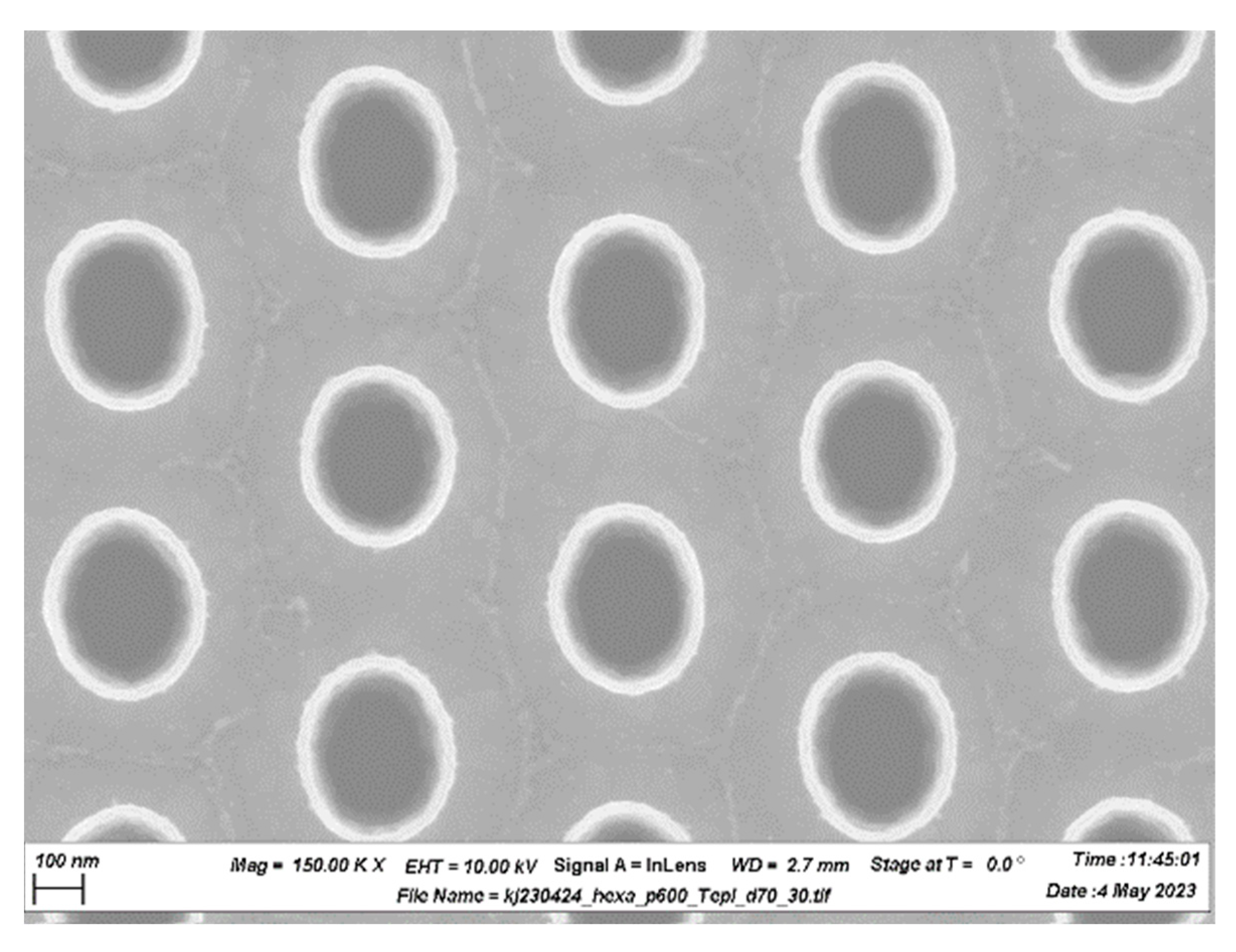
2.1. Nanofabrication

The plasmonic nanohole array was fabricated by displacement Talbot lithography [49]. An 80 nm Gold layer was deposited by thermal evaporation on a round polished glass wafer. A positive photoresist was deposited by spin coating onto the Gold layer. At this point, the sample was exposed to coherent UV light (377 nm) by irradiating a phase mask patterned with a hexagonal array of circular holes with a 600 nm pitch. The movement of the sample support stage allows the formation of holes with an elliptical shape. Argon milling and then Oxygen plasma etching was used to open the holes and to remove the residual photoresist, respectively. The final structure consists of a plasmonic nanohole array made of air holes etched in a Gold layer onto a glass substrate. A SEM image of the plasmonic nanohole array is reported in Figure 1. The estimated minor and major axis lengths of the elliptical holes are 340 nm and 274 nm, respectively.

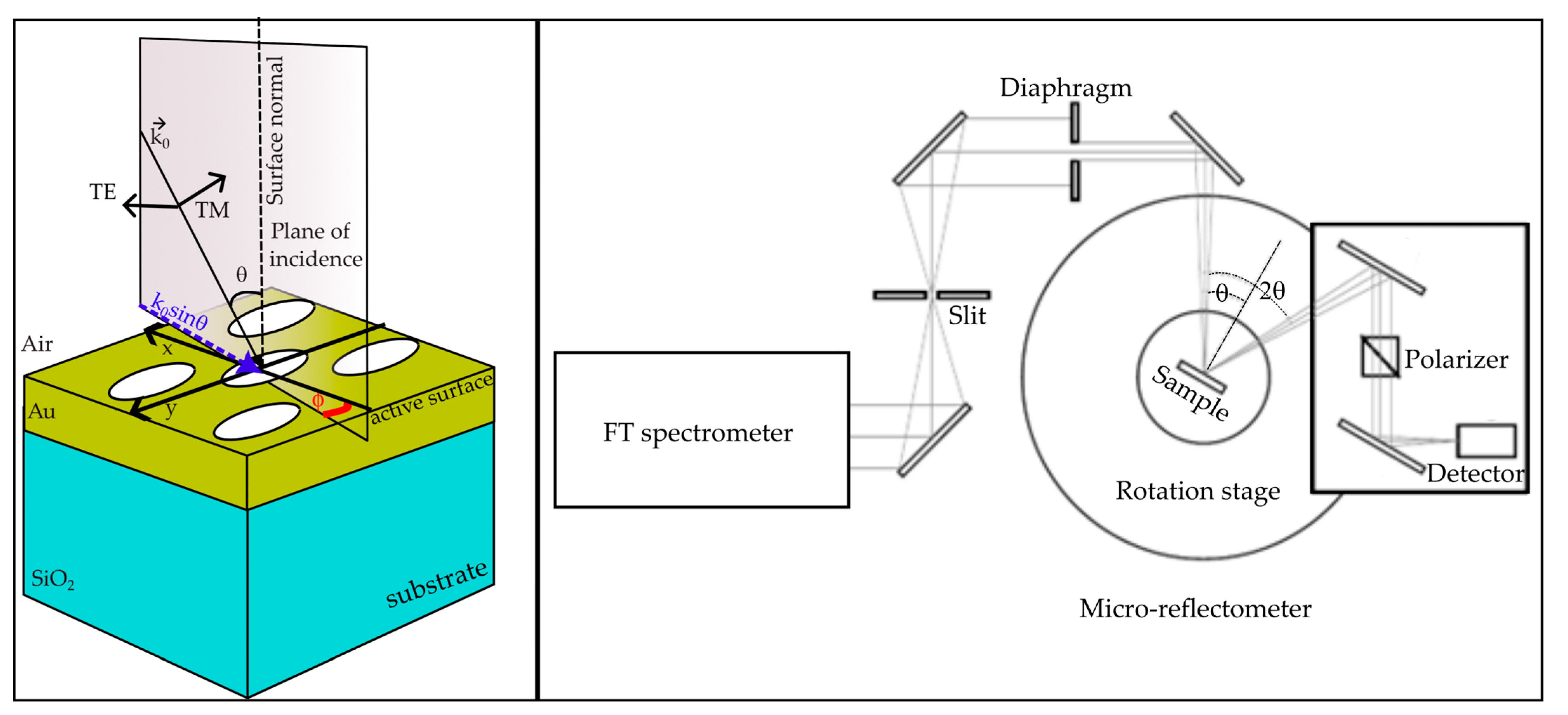
2.2. Optical Characterization
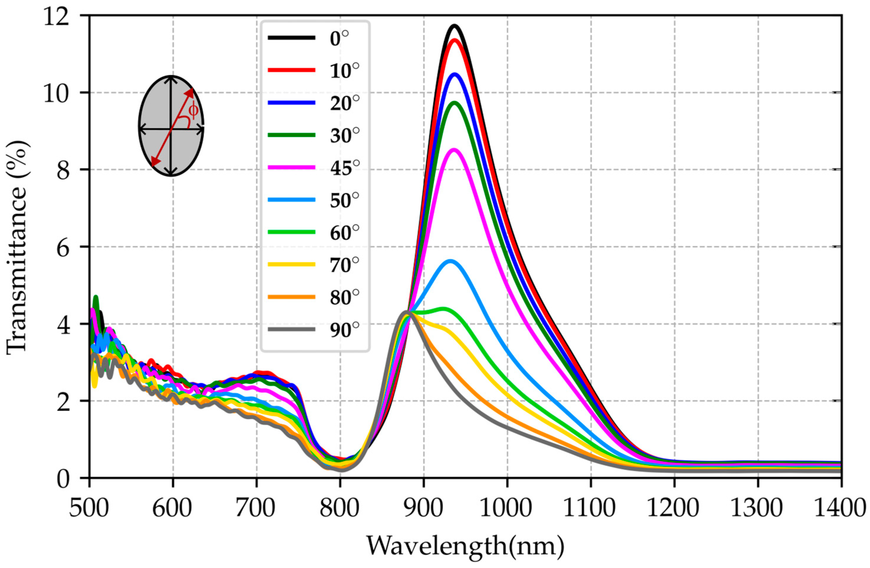
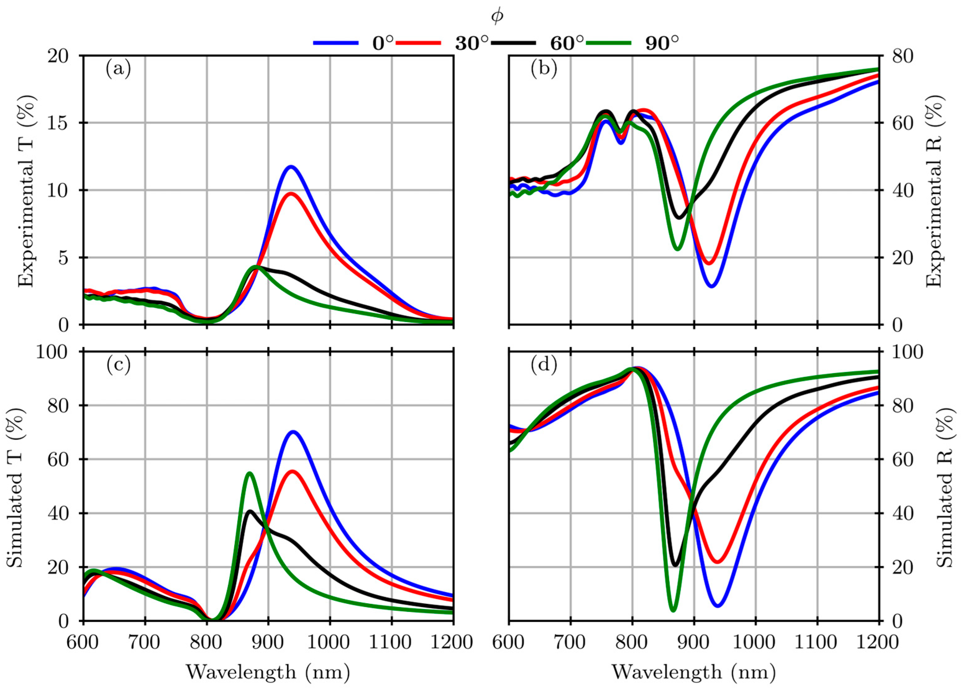
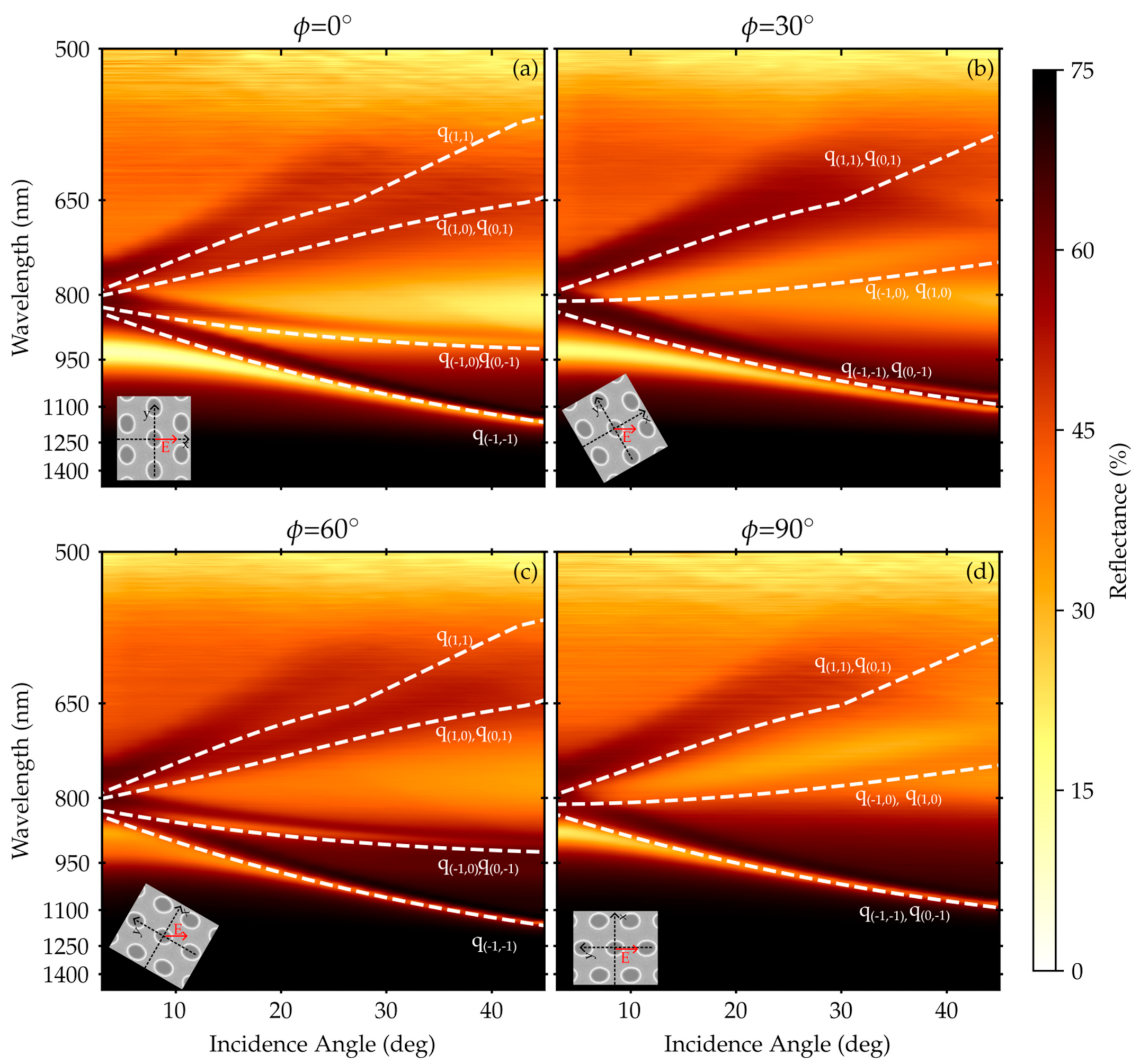
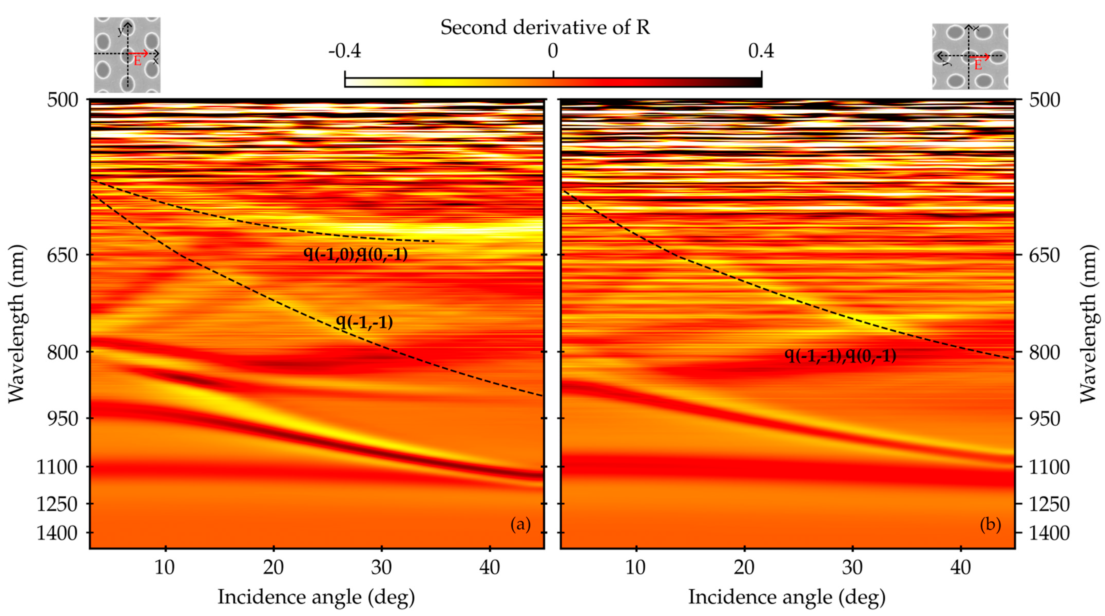
The scheme of the plasmonic nanohole array structure and the sketch of the optical configuration are reported in the left panel of Figure 2. For the measurement, the sample was placed orienting the minor axis of the ellipses along the x direction (left panel of Figure 2), defining the azimuthal angle ϕ equal to 0°.
The optical characterization was performed using a commercial Fourier-Transform (FT) spectrometer (Bruker IFS66s, Bruker Optics GmbH & Co. KG, Ettlingen, Germany) coupled with a micro reflectometer allowing variable-angle R and T measurements. The scheme of the spectroscopic setup is depicted in the right panel of Figure 2. The electromagnetic radiation exiting the FT spectrometer is collected by a mirror and focused onto a slit to shrink the spot size down to tenths of microns. Then, a diaphragm selects the beam aperture to be focused onto the sample, which is placed onto an XYZ translator (Mitutoyo, Kawasaki, Japan) and a rotation stage at the same time. The rotation stage allows the variation of the incidence angle θ of the light beam.
The homemade sample holder also enables the rotation of the sample with respect to the surface normal by an azimuthal angle ϕ, defined in the left panel of Figure 2. The sample surface is visualized by a camera, enabling the correct positioning of the sample on the axis of rotation, and selecting the surface area to investigate. Then, the reflected or transmitted beam is sent by a mirror on a Glan-Taylor polarizer (Thorlabs, Newton, NJ, USA) to select TM (electric field in the plane of incidence) or TE (electric field normal to the plane of incidence) polarization components, as depicted in Figure 2, and then sent to the detector. The whole detection part is placed onto a rotation stage allowing the detection of R in a specular-reflectance configuration.
For our study, a standard halogen lamp (Philips, Amsterdam, The Netherlands) was used as a source and a liquid Nitrogen-cooled InSb detector (Teledyne Judson Technologies, Montgomeryville, PA, USA) to measure the spectra in the range from 500 to 1400 nm with a 16 cm−1 resolution. The size of the spot used to investigate the sample surface was roughly 300 × 300 µm2, while the angular divergence of the light cone was 1°.
Normal incidence T and R spectral measurements were done by rotating the sample at different angles ϕ with TM-polarized light. Variable-angle R measurements were performed for θ from 3° to 45° with a 2° step for each of the azimuthal angles ϕ = 0°, 30°, 60° and 90° with TM-polarized light impinging from the sample SiO2 substrate. This configuration, which is leaving the active side of the plasmonic nanohole array free from the light beam, is the one adopted to couple the plasmonic modes in a convenient way for sensing applications [6].
Thanks to the surface periodicity, the electromagnetic radiation impinging on the nanohole array is directly coupled with both surface plasmon polaritons (SPPs) and localized surface plasmons (LSPR) [21,24,51]. Their fingerprints can be recognized in the reflectance (R) and/or transmittance (T) spectral features. By changing the incidence angle, as defined in the left panel of Figure 2, the in-plane wavevector component is varied and its energy dispersion can be mapped [20,38,52].

3. Results

Figure 3 reports the measured normal incidence (θ = 0°) T for azimuthal angle ϕ spanning from 0 to 90° with fixed TM polarization orientation. The rotation of the azimuthal angles changes the direction of polarization of the electric field with respect to both the two axes of the ellipsoidal holes and the orientation of the periodic arrangement, which has instead a sixfold symmetry.
For this reason, we expect to observe distinct effects of the rotation of the electric field on both the LSPR and SPPs due to their different nature.
A T minimum is observed near 800 nm in the whole set of data. This feature is the fingerprint of the plasmonic band gap, and it is strictly determined by the array pitch [20,24,38,52]. Instead, for both larger and smaller wavelengths absorption features can be observed. Starting from 0°, the T spectral features experience a progressive shift of the spectral weight towards lower wavelengths together with an intensity decrease. At ϕ = 0°, when the electric field component is aligned with the minor axis of the ellipse, a peak at 940 nm is observed. On the other hand, when the electric field is polarized along the major axis of the ellipse (at ϕ = 90°) the main resonance is located at 880 nm.
As soon as the orientation is changed, moving from the minor- towards the major- axis, the intensity of the peak at 940 nm decreases. A shoulder in T appears around 880 nm at 50°, showing an increasing weight until the peak at 940 disappears when the electric field is polarized along the major axis. This behavior can be ascribed to the different electromagnetic features of the LSPR excited by the electric field oscillation along the ellipse axes with the higher or lower dimensions. In fact, the hole shape and symmetry strongly influence the LSPR spectral shape and position, as well assessed in the literature [36,37,39,40]. At intermediate values of the azimuthal angle, when the electric field polarization angle lies between the two-fold elliptical symmetry directions (0° and 90°), both LSPR modes can be excited and a mixed response with two peaks can be observed.
The same effect can be found in the evolution of the near-normal incidence R spectra as a function of ϕ and it is also confirmed by Finite-difference time-domain (FDTD) simulations. In Figure 4 we report the experimental T and R spectra together with the simulated ones (the details can be found in Appendix A). Good consistency can be found between the experimental and simulated spectra apart from an overestimation of the T intensity. The low T experimental values could be due to a non-totally etched hole in the gold layer. As visible in Figure 4b, the R spectra exhibit complementary features to the T ones. At ϕ = 0°, a minimum in R, related to the LSPR excitation, is located near 940 nm. As ϕ is increased to 30°, which corresponds to the second azimuthal direction of the sixfold hexagonal lattice geometry, the resonance position does not change, except from a slight shoulder near 880 nm. When rotating the sample by other 30°, for ϕ = 60°, the R minimum exhibits a marked blue-shift towards the second LSPR at 880 nm, and a bigger shoulder can be noticed near 940 nm. Finally, for ϕ = 90°, the R minimum position is located at 880 nm. Overall, the observed behavior in the R and T spectra can be attributed mainly to the orientation of the electric field with respect to the ellipse axes, whereas no signatures can be retrieved related to the sixfold hexagonal lattice symmetry. In fact, the optical properties related to the array symmetry should display a change every 30° and be retrieved every 60°.

4. Discussion

To disentangle the effect of the hole shape-induced symmetry and the lattice symmetry on the plasmonic response of the nanohole array, we decided to study the dependence of the optical response on the incidence angle for different azimuthal orientations. In this way, not only the orientation of the electric field with respect to both the ellipse axes and the lattice symmetry directions is changed, but also the in-plane wavevector component, enabling to look at the SPPs dispersion. In Figure 5 the maps of the R spectra as a function of the angle of incidence are reported. The spectra were measured by impinging from the substrate for the azimuthal angles corresponding to both the ellipse axes (0° and 90°) and the ones of the 2D hexagonal lattice symmetry six-fold periodicity (30° and 60°).
If the electric field is oriented along the azimuthal direction of the hexagonal lattice (ϕ = 0°), several dispersive features in correspondence with the R minima can be recognized. They are the signature of the SPP resonant coupling at the Au/SiO2 interface of the plasmonic nanohole array. A main structure starting at normal incidence from 940 nm, is red-shifted at higher angles up to 1100 nm. Concurrently, other spectral features with similar behaviour are present and they can be related to the different SPP branches coupled by the hexagonal array reciprocal lattice vectors. To better recognize them, the theoretical SPP dispersion curves have been superimposed on the data, according to the selected azimuthal orientation. They were calculated resorting to the model in [52] with the following equation:
E ( θ , ϕ ) = ħ c ε g o l d ( E ) + ε d ε g o l d E ε d k 0 ϕ sin θ + q m n
where εd represents the permittivity of the dielectric medium interfacing with the gold surface, qmn denotes the reciprocal lattice vectors for the hexagonal lattice, and k₀(Φ)sinθ is the in-plane wavevector of the incident light (Figure 2). Accounting for the degeneracy, for ϕ = 0°, the SPP branches are four [52]. As visible in Figure 5a, the theoretical curves follow the R minima dispersion with a good agreement. The discrepancy, especially at low angles, is related to the plasmonic band gap opening at the folding point (800 nm), determined by the array pitch (600 nm) and by the superimposed LSPR resonance. As a matter of fact, in this type of plasmonic arrays the LSPR and SPPs interact, generating hybrid modes with a more localized or propagating component depending on the spectral region under consideration [51]. The anti-crossing behavior occurring between 20° and 30° of incidence angle around 800 nm is a consequence of such an interaction.
The low dispersion feature related to LSPR can be traced at about 940 nm at the lowest angles (as observed before) and around 880 nm at the highest ones. When the azimuthal orientation is changed to 30°, as reported in 5b, the contribution of such a localized resonance is only slightly modified consistently with our results presented in Section 3, whereas the SPP branches reduce to three with a different energy dispersion. Anyway, there is a good agreement between the theoretical curves and the evolution of the spectral features. By moving to 60° (Figure 5c) several effects are worth noticing. Firstly, at the lowest angles, the R minimum at normal incidence is blue shifted towards 880 nm, and its intensity has lowered. Correspondingly, the LSPR feature at the highest angles is broadened and blue shifted to 780 nm. On the other hand, the visible dispersive features return to be four and the overall behavior is similar to the one at ϕ = 0°. The dispersive part of the plasmonic response is recovered every 60°, consistently with the sixfold symmetry of the hexagonal lattice which is responsible for the SPP grating coupling. In fact, by implying an additional rotation of 30° and moving to 90°, the electric field polarization is oriented with respect to the major ellipse axis (Figure 5d), resulting in a blue-shift of the LSPR component at normal incidence. The SPP dispersion branches become three, as for 30°, the polarization being oriented with respect to the second azimuthal direction of the hexagonal lattice. As visible, even in this case the nondispersive structure arising in the plasmonic band gap shows an anti-crossing behavior, near the angle of incidence 10°.
At this point, the attention has been drawn only to the SPPs propagating at the Au/SiO2 interface of the plasmonic nanohole array, but these effects can also be studied by looking at the Au/air polaritons. These modes can be better visualized in the spectral features of variable-angle R impinging from the front side of the plasmonic nanohole array. Their folding point according to Equation (1), with an array pitch of 600 nm, falls near 550 nm where the gold reflectivity is decreasing and the efficiency of the used InSb detector is becoming poor. For this reason, their spectral fingerprints are not so marked with respect to the Au/SiO2 polaritons. To provide a better visualization of their dispersion, Figure 6 reports the second derivative of the R spectra as a function of the angles of incidence. Figure 6a shows the spectra for the azimuthal direction corresponding to the electric field polarization aligned with the minor axis of the ellipse, which also is the symmetry direction ϕ = 0° of the hexagonal lattice. A major SPP branch with corresponding qmn indexes (−1, −1) according to Equation (1), starting from 600 nm, is clearly visible in the maps. The (−1, 0), (0, −1) double degenerate branch, at higher energies, becomes more visible from 10°. Even if we expect to observe four branches, the two highest energy ones fall outside the detection region. It is worth noticing that the Au/SiO2 SPPs features are visible even if the measurement is performed from the front side of the plasmonic nanohole array, starting at the lowest angles at 940 nm. The plasmonic band gap related to the Au/SiO2 polaritons is still present at 800 nm, together with the four branches expected for ϕ = 0°. In fact, the air holes in the plasmonic array enable not only the grating coupling of the SPPs, but also the resonant interaction of the SPPs at the opposite interface [23]. If the sample is tilted by 90°, the electric field becomes parallel to the major ellipse axis, and it also corresponds to the second azimuthal direction of the hexagonal lattice (30°). Consistently and in analogy with the results in Figure 5, in of Figure 6b we observe the (−1, 1), (0, −1) SPP branch of Au/air polaritons. It becomes difficult to distinguish the other expected (1, 0), (−1, 0) central SPP branch and the upper one due to the decrease in the R intensity in this spectral region. In addition, the fingerprints of the Au/SiO2 SPP can be traced also in this case together with the LSPR resonance at the lowest angles at 880 nm, consistently with the findings in the Results section.

5. Conclusions

The complete optical characterization of a gold nanohole array fabricated by DTL has been performed. The studied sample has been a triangular lattice of elliptical holes. The results, compared with numerical simulations of an ideal structure, demonstrate the good quality and uniformity of the array. The plasmonic effects related to the local elliptical symmetry derived by the hole shape and the long-range one coming from the hexagonal lattice have been disentangled and analyzed. The influence of the elliptical hole shape is visible in the near-normal incidence reflectance and transmittance spectra, showing a recurrent behavior consistent with the twofold symmetry. On the other hand, the propagating part of the plasmonic excitation is mainly affected by the hexagonal lattice symmetry. The dispersion features are in fact consistent with the hexagonal lattice sixfold symmetry, independently on the alignment of the ellipse axes with the electric field polarization. It is worth noticing that, to the best of our knowledge, such a comprehensive analysis has been performed on the same sample in just one work. In addition, due to the elliptical axes aligned along the symmetry axes of the array, only non-chiral and non-dichroic effects were revealed. Then, these results represent a reference point for the future study of non-isotropic effects, such as dichroism, in structures where this kind of alignment is missing. By a careful tailoring of the alignment and shape of the holes with respect to the lattice symmetry directions, made possible by the newly presented nanofabrication technique, new potential cutting edge studies and applications could be explored, involving enhanced chirality and moving towards plasmonic bound states in the continuum [46,47,48].

Author Contributions

Conceptualization, F.M., M.A. and F.F.; methodology, F.M. and M.A.; software, M.A.; validation, M.A., F.F. and F.M.; formal analysis, M.A.; investigation, F.M. and M.A.; resources, K.J.; data curation, M.A. and F.M.; writing—original draft preparation, M.A. and F.M.; writing—review and editing, M.A., F.M., K.J. and F.F.; visualization, M.A., F.M. and F.F.; supervision, F.F. and F.M.; project administration, P.P., D.K. and F.F.; funding acquisition, P.P., D.K. and F.F. All authors have read and agreed to the published version of the manuscript.

Funding

This research was founded from the EU’s H2020 framework program for research and innovation under grant agreement NFFA-Europe-Pilot (n. 101007417 from 1 March 2021 to 28 February 2026), by SNF R’Equip grant 206021_177036/1 “Displacement Talbot Lithography for micro and nanopatterning”, and by the European Union—FSE REACT-EU, PON Ricerca e Innovazione 2014–2020, funding number F11B21009090007.

Institutional Review Board Statement

Not applicable.

Informed Consent Statement

Not applicable.

Data Availability Statement

Data are contained within the article.

Conflicts of Interest

Paola Pellacani is employed by Plasmore Srl. The remaining authors declare that the research was conducted in the absence of any commercial or financial relationships that could be construed as a potential conflict of interest.

Appendix A. Finite-Difference Time-Domain Simulations

The structural model of the plasmonic nanohole array was built in Ansys Lumerical FDTD [53] resorting to nanofabrication parameters and SEM images. The gold film optical properties were set as the built-in Johnson and Christy data from the material database, while SiO2 and air were modeled as perfect dielectric materials selecting a refractive index of 1.5 and 1.0, respectively. A plane wave source embedded in the SiO2 substrate was employed to illuminate the structure at normal incidence within the wavelength range of 600 to 1200 nm. Two frequency-domain field and power monitors, positioned below the Au/SiO2 interface and above it, were used to calculate R and T spectra within the same spectral range. Simulations were conducted for polarization angles of the electric field of the source with respect to the x-axis at 0°, 30°, 60°, and 90°, which was aligned with the major axis of the elliptical hole. The simulations were run on a liquid-cooled Intel® (Santa Clara, CA, USA) Core 12th generation i9-12900K (16 core) with 128 GB of DDR5-RAM. An average simulation time of about 3 min was required.

References

  1. Yang, K.; Yao, X.; Liu, B.; Ren, B. Metallic Plasmonic Array Structures: Principles, Fabrications, Properties, and Applications. Adv. Mater. 2021, 33, 2007988. [Google Scholar] [CrossRef] [PubMed]
  2. Maier, S.A. Plasmonics: Fundamentals and Applications; Springer: New York, NY, USA, 2007; ISBN 978-0-387-33150-8. [Google Scholar]
  3. García De Abajo, F.J. Colloquium: Light Scattering by Particle and Hole Arrays. Rev. Mod. Phys. 2007, 79, 1267–1290. [Google Scholar] [CrossRef]
  4. Sun, L.L.; Leo, Y.S.; Zhou, X.; Ng, W.; Wong, T.I.; Deng, J. Localized Surface Plasmon Resonance Based Point-of-Care System for Sepsis Diagnosis. Mater. Sci. Energy Technol. 2020, 3, 274–281. [Google Scholar] [CrossRef]
  5. Escobedo, C. On-Chip Nanohole Array Based Sensing: A Review. Lab. Chip 2013, 13, 2445. [Google Scholar] [CrossRef] [PubMed]
  6. Bottazzi, B.; Fornasari, L.; Frangolho, A.; Giudicatti, S.; Mantovani, A.; Marabelli, F.; Marchesini, G.; Pellacani, P.; Therisod, R.; Valsesia, A. Multiplexed Label-Free Optical Biosensor for Medical Diagnostics. J. Biomed. Opt. 2014, 19, 017006. [Google Scholar] [CrossRef] [PubMed]
  7. Liang, Y.; Lin, H.; Lin, S.; Wu, J.; Li, W.; Meng, F.; Yang, Y.; Huang, X.; Jia, B.; Kivshar, Y. Hybrid Anisotropic Plasmonic Metasurfaces with Multiple Resonances of Focused Light Beams. Nano Lett. 2021, 21, 8917–8923. [Google Scholar] [CrossRef] [PubMed]
  8. Angelini, M.; Manobianco, E.; Pellacani, P.; Floris, F.; Marabelli, F. Plasmonic Modes and Fluorescence Enhancement Coupling Mechanism: A Case with a Nanostructured Grating. Nanomaterials 2022, 12, 4339. [Google Scholar] [CrossRef] [PubMed]
  9. Bauch, M.; Toma, K.; Toma, M.; Zhang, Q.; Dostalek, J. Plasmon-Enhanced Fluorescence Biosensors: A Review. Plasmonics 2014, 9, 781–799. [Google Scholar] [CrossRef]
  10. Brolo, A.G.; Kwok, S.C.; Moffitt, M.G.; Gordon, R.; Riordon, J.; Kavanagh, K.L. Enhanced Fluorescence from Arrays of Nanoholes in a Gold Film. J. Am. Chem. Soc. 2005, 127, 14936–14941. [Google Scholar] [CrossRef]
  11. Guo, P.-F.; Wu, S.; Ren, Q.-J.; Lu, J.; Chen, Z.; Xiao, S.-J.; Zhu, Y.-Y. Fluorescence Enhancement by Surface Plasmon Polaritons on Metallic Nanohole Arrays. J. Phys. Chem. Lett. 2010, 1, 315–318. [Google Scholar] [CrossRef]
  12. Cui, X.; Tawa, K.; Hori, H.; Nishii, J. Tailored Plasmonic Gratings for Enhanced Fluorescence Detection and Microscopic Imaging. Adv. Funct. Mater. 2010, 20, 546–553. [Google Scholar] [CrossRef]
  13. Liu, Y.; Blair, S. Fluorescence Enhancement from an Array of Subwavelength Metal Apertures. Opt. Lett. 2003, 28, 507. [Google Scholar] [CrossRef] [PubMed]
  14. Cialla, D.; März, A.; Böhme, R.; Theil, F.; Weber, K.; Schmitt, M.; Popp, J. Surface-Enhanced Raman Spectroscopy (SERS): Progress and Trends. Anal. Bioanal. Chem. 2012, 403, 27–54. [Google Scholar] [CrossRef] [PubMed]
  15. Hering, K.; Cialla, D.; Ackermann, K.; Dörfer, T.; Möller, R.; Schneidewind, H.; Mattheis, R.; Fritzsche, W.; Rösch, P.; Popp, J. SERS: A Versatile Tool in Chemical and Biochemical Diagnostics. Anal. Bioanal. Chem. 2008, 390, 113–124. [Google Scholar] [CrossRef] [PubMed]
  16. Huang, X.; Tian, H.; Huang, L.; Chen, Q.; Yang, Y.; Zeng, R.; Xu, J.; Chen, S.; Zhou, X.; Liu, G.; et al. Well-Ordered Au Nanoarray for Sensitive and Reproducible Detection of Hepatocellular Carcinoma-Associated miRNA via CHA-Assisted SERS/Fluorescence Dual-Mode Sensing. Anal. Chem. 2023, 95, 5955–5966. [Google Scholar] [CrossRef] [PubMed]
  17. Gu, Y.; Zhang, L.; Yang, J.K.W.; Yeo, S.P.; Qiu, C.-W. Color Generation via Subwavelength Plasmonic Nanostructures. Nanoscale 2015, 7, 6409–6419. [Google Scholar] [CrossRef]
  18. Raj Shrestha, V.; Lee, S.-S.; Kim, E.-S.; Choi, D.-Y. Polarization-Tuned Dynamic Color Filters Incorporating a Dielectric-Loaded Aluminum Nanowire Array. Sci. Rep. 2015, 5, 12450. [Google Scholar] [CrossRef]
  19. Ellenbogen, T.; Seo, K.; Crozier, K.B. Chromatic Plasmonic Polarizers for Active Visible Color Filtering and Polarimetry. Nano Lett. 2012, 12, 1026–1031. [Google Scholar] [CrossRef] [PubMed]
  20. Ebbesen, T.W.; Lezec, H.J.; Ghaemi, H.F.; Thio, T.; Wolff, P.A. Extraordinary Optical Transmission through Sub-Wavelength Hole Arrays. Nature 1998, 391, 667–669. [Google Scholar] [CrossRef]
  21. Degiron, A.; Ebbesen, T.W. The Role of Localized Surface Plasmon Modes in the Enhanced Transmission of Periodic Subwavelength Apertures. J. Opt. A Pure Appl. Opt. 2005, 7, S90–S96. [Google Scholar] [CrossRef]
  22. Liu, H.; Lalanne, P. Microscopic Theory of the Extraordinary Optical Transmission. Nature 2008, 452, 728–731. [Google Scholar] [CrossRef]
  23. Martín-Moreno, L.; García-Vidal, F.J.; Lezec, H.J.; Pellerin, K.M.; Thio, T.; Pendry, J.B.; Ebbesen, T.W. Theory of Extraordinary Optical Transmission through Subwavelength Hole Arrays. Phys. Rev. Lett. 2001, 86, 1114–1117. [Google Scholar] [CrossRef] [PubMed]
  24. Barnes, W.L.; Murray, W.A.; Dintinger, J.; Devaux, E.; Ebbesen, T.W. Surface Plasmon Polaritons and Their Role in the Enhanced Transmission of Light through Periodic Arrays of Subwavelength Holes in a Metal Film. Phys. Rev. Lett. 2004, 92, 107401. [Google Scholar] [CrossRef]
  25. Martin-Moreno, L.; Garcia-Vidal, F.J. Optical Transmission through Circular Hole Arrays in Optically Thick Metal Films. Opt. Express 2004, 12, 3619–3628. [Google Scholar] [CrossRef]
  26. Sepúlveda, B.; Alaverdyan, Y.; Alegret, J.; Käll, M.; Johansson, P. Shape Effects in the Localized Surface Plasmon Resonance of Single Nanoholes in Thin Metal Films. Opt. Express 2008, 16, 5609. [Google Scholar] [CrossRef] [PubMed]
  27. Degiron, A.; Lezec, H.J.; Barnes, W.L.; Ebbesen, T.W. Effects of Hole Depth on Enhanced Light Transmission through Subwavelength Hole Arrays. Appl. Phys. Lett. 2002, 81, 4327–4329. [Google Scholar] [CrossRef]
  28. Mary, A.; Rodrigo, S.G.; Martín-Moreno, L.; García-Vidal, F.J. Theory of Light Transmission through an Array of Rectangular Holes. Phys. Rev. B 2007, 76, 195414. [Google Scholar] [CrossRef]
  29. Genet, C.; Ebbesen, T.W. Light in Tiny Holes. Nature 2007, 445, 39–46. [Google Scholar] [CrossRef]
  30. Garcia-Vidal, F.J.; Martin-Moreno, L.; Ebbesen, T.W.; Kuipers, L. Light Passing through Subwavelength Apertures. Rev. Mod. Phys. 2010, 82, 729–787. [Google Scholar] [CrossRef]
  31. Shafiq, R.; Khan, A.D.; Al-Harbi, F.F.; Ali, F.; Armghan, A.; Asif, M.; Rehman, A.U.; Ali, E.M.; Arpanaei, F.; Alibakhshikenari, M.; et al. Optical Transmission Plasmonic Color Filter with Wider Color Gamut Based on X-Shaped Nanostructure. Photonics 2022, 9, 209. [Google Scholar] [CrossRef]
  32. Wang, Y.; Qin, Y.; Zhang, Z. Extraordinary Optical Transmission Property of X-Shaped Plasmonic Nanohole Arrays. Plasmonics 2014, 9, 203–207. [Google Scholar] [CrossRef]
  33. Balaur, E.; Sadatnajafi, C.; Kou, S.S.; Lin, J.; Abbey, B. Continuously Tunable, Polarization Controlled, Colour Palette Produced from Nanoscale Plasmonic Pixels. Sci. Rep. 2016, 6, 28062. [Google Scholar] [CrossRef] [PubMed]
  34. Langley, D.; Balaur, E.; Sadatnajafi, C.; Abbey, B. Dual Pitch Plasmonic Devices for Polarization Enhanced Colour Based Sensing. In SPIE BioPhotonics Australasia, Proceedings of the SPIE Biophotonics Australasia 2016, Adelaide, Australia, 16–19 October 2016; Hutchinson, M.R., Goldys, E.M., Eds.; SPIE Digital Library: Bellingham, WA, USA, 2016; p. 1001338. [Google Scholar]
  35. Sadatnajafi, C.; Balaur, E.; Abbey, B. Bimodal Plasmonic Color Filters Enable Direct Optical Imaging of Ion Implantation in Thin Films. Adv. Funct. Mater. 2022, 32, 2009419. [Google Scholar] [CrossRef]
  36. Gordon, R.; Brolo, A.G.; McKinnon, A.; Rajora, A.; Leathem, B.; Kavanagh, K.L. Strong Polarization in the Optical Transmission through Elliptical Nanohole Arrays. Phys. Rev. Lett. 2004, 92, 037401. [Google Scholar] [CrossRef]
  37. Gordon, R.; Hughes, M.; Leathem, B.; Kavanagh, K.L.; Brolo, A.G. Basis and Lattice Polarization Mechanisms for Light Transmission through Nanohole Arrays in a Metal Film. Nano Lett. 2005, 5, 1243–1246. [Google Scholar] [CrossRef]
  38. Li, J.; Iu, H.; Wan, J.T.K.; Ong, H.C. The Plasmonic Properties of Elliptical Metallic Hole Arrays. Appl. Phys. Lett. 2009, 94, 033101. [Google Scholar] [CrossRef]
  39. Strelniker, Y.M. Theory of Optical Transmission through Elliptical Nanohole Arrays. Phys. Rev. B 2007, 76, 085409. [Google Scholar] [CrossRef]
  40. Wu, S.; Zhou, L.; Wang, Y.; Wang, G.; Wang, Q.; Huang, C.; Zhu, Y. Optical Properties of a Metal Film Perforated with Coaxial Elliptical Hole Arrays. Phys. Rev. E 2010, 81, 057601. [Google Scholar] [CrossRef]
  41. Ai, B.; Basnet, P.; Larson, S.; Ingram, W.; Zhao, Y. Plasmonic Sensor with High Figure of Merit Based on Differential Polarization Spectra of Elliptical Nanohole Array. Nanoscale 2017, 9, 14710–14721. [Google Scholar] [CrossRef]
  42. Lovera, P.; Jones, D.; O’Riordan, A. Elliptical Nanohole Array in Thin Gold Film as Micrometer Sized Optical Filter Set for Fluorescent-Labelled Assays. J. Phys. Conf. Ser. 2011, 307, 012006. [Google Scholar] [CrossRef]
  43. Petronijevic, E.; Belardini, A.; Leahu, G.; Cesca, T.; Scian, C.; Mattei, G.; Sibilia, C. Circular Dichroism in Low-Cost Plasmonics: 2D Arrays of Nanoholes in Silver. Appl. Sci. 2020, 10, 1316. [Google Scholar] [CrossRef]
  44. Ali, H.; Petronijevic, E.; Pellegrini, G.; Sibilia, C.; Andreani, L.C. Circular Dichroism in a Plasmonic Array of Elliptical Nanoholes with Square Lattice. Opt. Express 2023, 31, 14196. [Google Scholar] [CrossRef]
  45. Petronijevic, E.; Ghahri, R.; Sibilia, C. Plasmonic Elliptical Nanohole Arrays for Chiral Absorption and Emission in the Near-Infrared and Visible Range. Appl. Sci. 2021, 11, 6012. [Google Scholar] [CrossRef]
  46. Aigner, A.; Tittl, A.; Wang, J.; Weber, T.; Kivshar, Y.; Maier, S.A.; Ren, H. Plasmonic Bound States in the Continuum to Tailor Light-Matter Coupling. Sci. Adv. 2022, 8, eadd4816. [Google Scholar] [CrossRef]
  47. Zagaglia, L.; Zanotti, S.; Minkov, M.; Liscidini, M.; Gerace, D.; Claudio Andreani, L. Polarization States and Far-Field Optical Properties in Dielectric Photonic Crystal Slabs. Opt. Lett. 2023, 48, 5017. [Google Scholar] [CrossRef]
  48. Tang, Y.; Liang, Y.; Yao, J.; Chen, M.K.; Lin, S.; Wang, Z.; Zhang, J.; Huang, X.G.; Yu, C.; Tsai, D.P. Chiral Bound States in the Continuum in Plasmonic Metasurfaces. Laser Photonics Rev. 2023, 17, 2200597. [Google Scholar] [CrossRef]
  49. Solak, H.H.; Dais, C.; Clube, F. Displacement Talbot Lithography: A New Method for High-Resolution Patterning of Large Areas. Opt. Express 2011, 19, 10686. [Google Scholar] [CrossRef] [PubMed]
  50. Balaur, E.; Sadatnajafi, C.; Abbey, B. Large-Scale Fabrication of Optically Active Plasmonic Arrays via Displacement Talbot Lithography. J. Phys. Conf. Ser. 2020, 1455, 012005. [Google Scholar] [CrossRef]
  51. Giudicatti, S.; Marabelli, F.; Valsesia, A.; Pellacani, P.; Colpo, P.; Rossi, F. Interaction among Plasmonic Resonances in a Gold Film Embedding a Two-Dimensional Array of Polymeric Nanopillars. J. Opt. Soc. Am. B 2012, 29, 1641. [Google Scholar] [CrossRef]
  52. Giudicatti, S.; Valsesia, A.; Marabelli, F.; Colpo, P.; Rossi, F. Plasmonic Resonances in Nanostructured Gold/Polymer Surfaces by Colloidal Lithography: Plasmonic Resonances in Nanostructured Gold/Polymer Surfaces. Phys. Status Solidi A 2010, 207, 935–942. [Google Scholar] [CrossRef]
  53. Lumerical Inc. Available online: https://www.Lumerical.Com/Products/Fdtd/ (accessed on 20 December 2023).
Figure 1. Scanning electron microscope image of the plasmonic nanohole array.
Optics 05 00014 g001
Figure 2. Left panel: a stack of the plasmonic nanohole array. The plane of incidence, together with the incidence angle θ and the azimuthal angle ϕ are defined. TM and TE polarization are indicated to define the location of the electric field component in the plane and normal to the plane of incidence, respectively. The in-plane wavevector component is indicated in blue. Right panel: scheme of the optical configuration of the experiment with a homemade micro-reflectometer.
Optics 05 00014 g002
Figure 3. Normal incidence (θ = 0°) T spectra acquired for different azimuthal angles ϕ. The spectra were acquired by impinging with light from the front side of the plasmonic nanohole array with TM polarized light (electric field component in the plane of incidence). The red arrow indicates the polarization of the electric field with respect to the ellipse axes.
Optics 05 00014 g003
Figure 4. Experimental (panels (a,b)) and simulated (panels (c,d)) normal incidence T and near-normal incidence (ϑ = 3°) R spectra for different azimuthal angles ϕ by impinging with light from the SiO2 substrate of the plasmonic nanohole array.
Optics 05 00014 g004
Figure 5. (ad) Variable-angle R spectra acquired impinging from the SiO2 substrate with TM polarized light rotating the sample by different azimuthal angles. The calculated SPP dispersions at the Au/SiO2 interface are superimposed on the spectra, together with the labels according to [52].
Optics 05 00014 g005
Figure 6. The second derivative of variable-angle R spectra for (ϕ = 0°) acquired impinging from the front side of the plasmonic nanohole array with TM polarized light. The calculated SPP dispersions at the Au/air interface are superimposed on the spectra, together with the labels according to [52].
Optics 05 00014 g006
Disclaimer/Publisher’s Note: The statements, opinions and data contained in all publications are solely those of the individual author(s) and contributor(s) and not of MDPI and/or the editor(s). MDPI and/or the editor(s) disclaim responsibility for any injury to people or property resulting from any ideas, methods, instructions or products referred to in the content.

