Abstract
Incorporating active components in photonic structures with a topological configuration has been shown to achieve lasing at topological edge states. Here, we report an electrically tunable topological edge-state laser in a one-dimensional complex Su–Schrieffer–Heeger chain. The proposed design is realized in an electrically injected Fabry–Perot (FP) laser chain. The lasing in topologically induced edge states is experimentally observed and a selective enhancement is realized by introducing a topological defect in the center. This work presents a versatile platform to investigate novel concepts such as the topological mode for mainstream photonic applications.
1. Introduction
Topological insulators (TIs) introduce a new form of matter, which can support the flow of electrons on their surface but are insulators on their interior. Dissimilar to surface states in normal insulators, the surface states in TIs are robust against perturbation and defects in the bulks [1,2,3,4,5,6]. Such tantalizing characteristics address the impurity issues in conventional bulk topology materials and spark interest in the field of topological photonics [7,8,9]. Thus, it has drawn large interest in the investigation of topological-phase transitions and edge states in optical devices such as lasers, that are sensitive to local perturbations and fabrication defects. Most such work has focused on optical structures and devices with passive components [10,11,12,13,14,15,16,17]. By incorporating active components in the photonic topological structures, it becomes possible to achieve lasing at the topological edge states. The resulting topological edge-state lasers can exhibit a low lasing threshold compared to the conventional bulk-state lasers, and are robust against fabrication defects and local defects. Topological edge-state lasers have recently been demonstrated in several systems [18,19,20,21,22,23]; however, all of them are shown in optically pumped platforms (bulky and slow), which can largely limit the further exploration and application of these unique topological lasers. On the other side, the optical non-Hermitian system with active elements has been brought to attention. Several new novel phenomena and optical devices have been proposed and demonstrated based on the PT symmetry in non-Hermitian systems [24,25,26,27,28,29,30,31,32,33,34]. Non-Hermiticity in photonics topology systems has been studied and experimentally demonstrated [24,25,26]. It was also found that, by introducing a defect site in the center of gain/loss sites, the topological midgap state can be enhanced by supplementing the topological protection with non-Hermitian symmetries [10]. In this context, topological lasers become an ideal platform owing to the inherent non-Hermiticity in laser structures. In this report, we demonstrate lasing in a topological edge state in a one-dimensional Su–Schrieffer–Heeger (SSH) Fabry–Perot (FP) laser chain, which contains gain and loss waveguides and an active gain topological defect. The active topological defect is employed to amplify the density of state (DOS) of the midgap states naturally induced by breaking the PT symmetry in the system. These states maintain their topological properties while presenting the lowest lasing threshold compared to other bulk modes. By tuning bias levels in gain/loss sites, the dynamic evolution of the dispersion relationship is studied, and the phase transition from the trivial state to topological state is manifested with incremental bias levels. Finally, from the interest of the symmetry of the proposed system, a reconfiguration of the gain/loss site, which is a time reversal of the original one, is studied. By electrically tuning the gain and loss in the SSH laser chain, lasing is also obtained in the SSH chain in the time-reversal configurations.
2. Model and Simulation
2.1. Non-Hermitian Topological Laser Chain
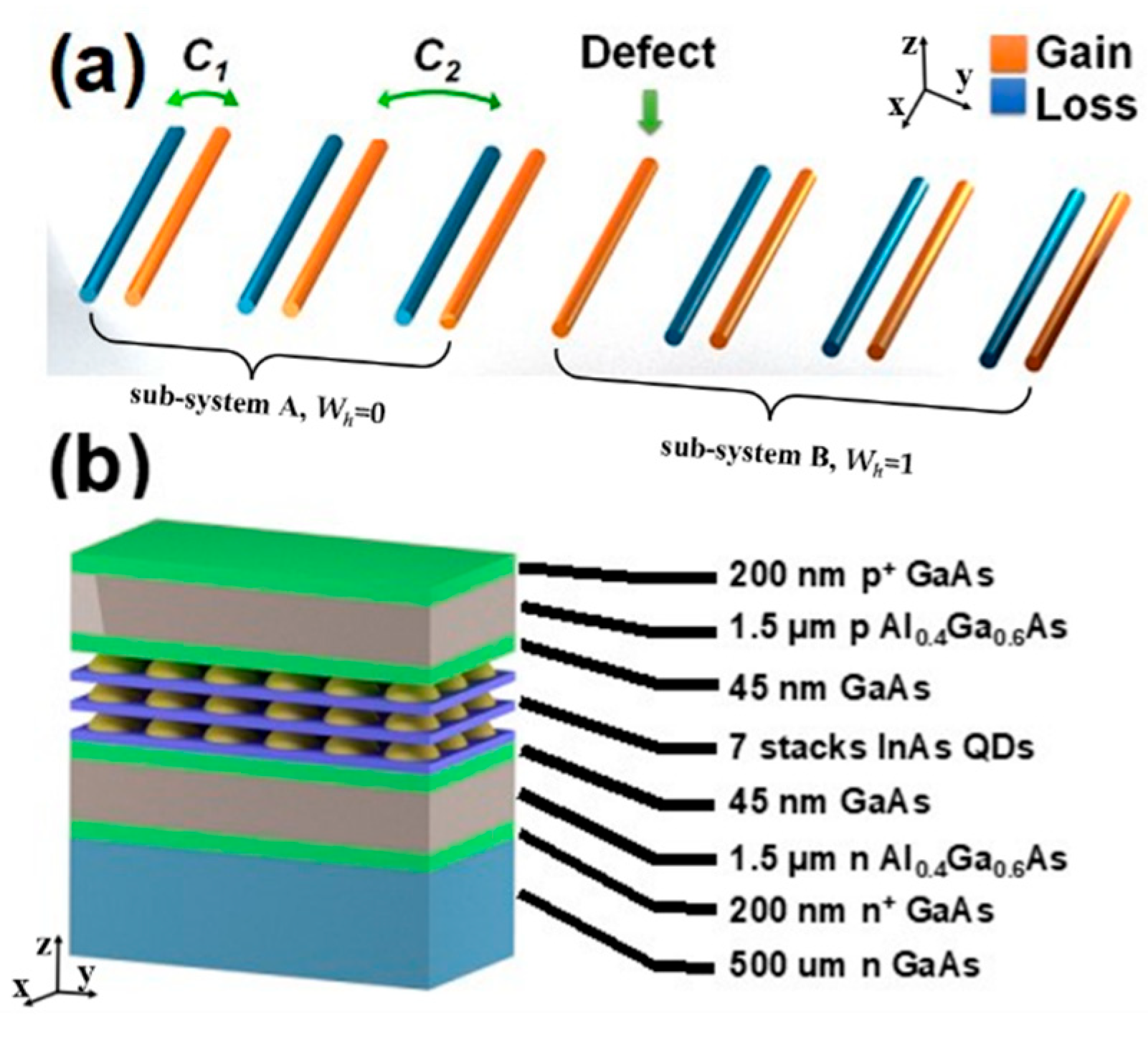
To achieve a photonic topological laser, we designed a photonic topological insulator structure consisting of seven pairs of coupled Fabry–Perot (FP) waveguide SSH dimers. Figure 1a shows the schematic of the dimer chain, where C1 and C2 represent the intradimer and interdimer coupling coefficients, respectively, and C1 > C2. The intradimer coupling denotes field coupling between the loss (blue) waveguides and the gain (orange) waveguides, and interdimer coupling denotes coupling between gain (orange) waveguides and next loss (blue) waveguides. The trivial and nontrivial topological states were achieved by the strong and weak coupling in the dimers consisting of a gain and loss, respectively. A topological defect in the chain was introduced by removing the loss waveguide in the middle dimer (fourth pair). As a result, the designed active SSH chain consisted of 13 coupled ridge waveguide lasers with a width of 3 µm. The laser active region was composed of seven-layer InAs quantum dots (QDs) sandwiched between Al0.4Ga0.6As cladding layers. Figure 1b shows the heterostructures of the InAs QD lasers grown by the molecular beam epitaxy (MBE) system. In the laser chain, the top p+-GaAs contact layer and p-Al0.4Ga0.6As cladding layer were etched for electrical isolation between each waveguide. The coupling strengths, C1 and C2, in the dimers were controlled by the width of the isolation trenches, 1 µm and 2 µm, respectively. All the gain and loss waveguides were interconnected, allowing the simultaneous and fully electrical control of all the gain and loss waveguides. A one-dimensional SSH model was first employed to investigate the passive Hermitian dimer chain without a gain and loss [35]. The SSH model studied two sites per unit cell with different coupling coefficients: intradimer coupling C1 and interdimer coupling C2. It is well understood that, in the SSH mode, the topological zero states depend on the configuration of the unit cell. The topological state exists only when the smaller coupling, C2, is located at the edges [35,36]. In contrast, there is no interface state if the chain is terminated by a dimer with a larger coupling coefficient, C1. These two different scenarios could be identified by the winding number in the Brillouin zone (BZ) SSH model [37]:
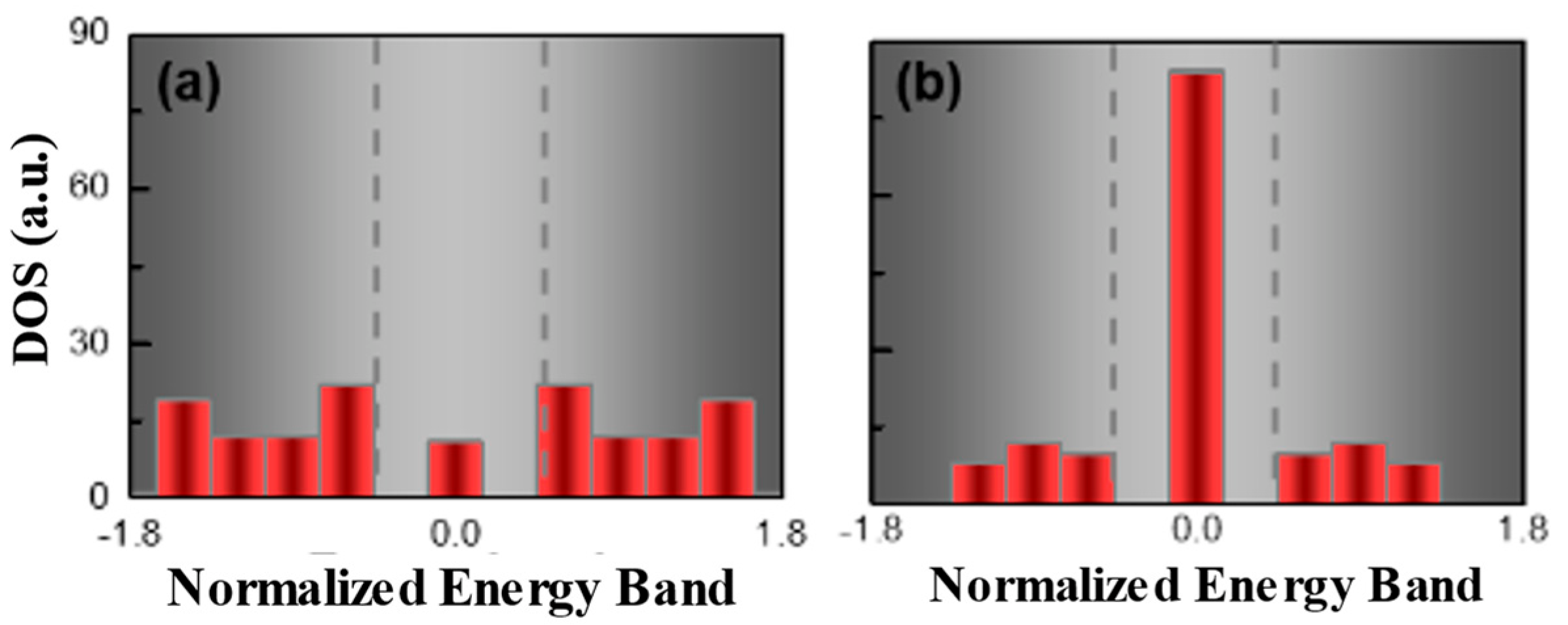
where k is the Bloch wavenumber within the first BZ and the winding number corresponds to the Zak phase (ψZAK) divided by π [38]. It has been shown that when Wh = 0, the system exhibits a trivial topological phase; in contrast, if Wh = 1, the system transits into a nontrivial topological phase [39]. In the explored topological configuration, as shown in Figure 1a, all sites in the left side of the center site could be treated as subsystem A, which had a winding number of 0, and the rest of the sites, including the center site and all the other sites on the right side of the center site, could be treated as subsystem B, which had a winding number of 1 due to the different bounded edge with the coupling coefficient C1 in the left and C2 in the right. To obtain the coupling coefficients and , the mode coupling between the waveguides was studied by the commercial software COMSOL. = 10.05 cm−1 and = 5.32 cm−1 were obtained from COMSOL simulations. A topological transition would occur from configuration A to B, where the winding number changed from 0 to 1; as a result, the defect waveguide, the fourth pair dimer with a gain waveguide only, was located at the interface. Therefore, there had to be a topological interface state residing at the zero energy band, located at the defect waveguide. Szameit et al. already investigated such a topological waveguide configuration containing passive components, and showed the topological mode appearing in the center defect while preserving the PT symmetry [40,41,42]. In this work, we employed the dimer chain containing a gain and loss and an active gain defect to achieve a topological laser. In this context, a modified non-Hermitian SSH model was employed to study the density of state (DOS) of the SSH laser chain. The DOS was calculated by evaluating the number of eigenstates at the corresponding eigenvalues in momentum space (see Supplementary Materials for details). As shown in Figure 2a, the DOS was calculated with a passive defect in the center and all modes were grouped into two sets and separated by the middle gap. Different from defect-less SSH chains, topologically induced states manifested in the middle of the gap, which resulted from the PT symmetry breaking in the system. By introducing a gain into the center defect, as shown in Figure 2b, topologically induced states in the midgap were amplified, while states in the upper and lower groups were suppressed. It is worth noting that the DOS enhancement could be obtained not only by introducing the active defect, but also by introducing an absorptive lossy defect as well due to the time symmetry of the Hamiltonian.

Figure 1.
(a) Schematic of the proposed non-Hermitian SSH dimer chain, with staggered gain (orange) and loss (blue) waveguides, except the center single defected gain waveguide. and represent the coupling coefficients for intradimer and interdimer, respectively, where > . (b) Heterostructures of the InAs QD lasers grown by molecular beam epitaxy.

Figure 2.
The density of states (DOS) of SSH chain without (a) and with (b) active defect, where the energy band was presented as normalized energy E/. In passive system (a), with zero gain, DOS of zero-energy states presented as less dominant compared to other bulk modes; on the contrary, in the active system (b), the DOS of the zero-energy mode was largely enhanced as a dominant mode by including an active defect.
2.2. Phase Transition of Non-Hermitian Topological Laser Chain
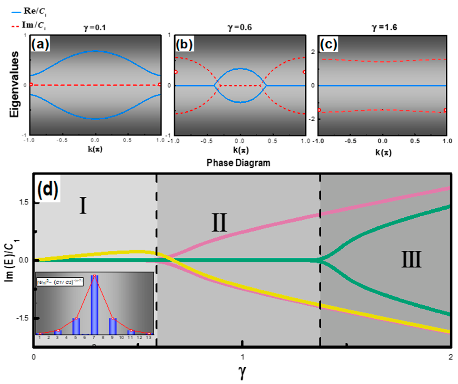
For characterizing trivial states and the topological state at different biasing levels, complex dispersion relations and eigenvalues of the SSH laser chain were analyzed. Three phases were employed to distinct degeneracy conditions of the eigenstates of the Hamiltonian. The explicit form of the Hamiltonian of the SSH chain was given in supplement, g represented the gain and loss in the SSH chain, and a was the scale factor of the gain in the defect site. In the case of this work, the scale a was set to one to provide a uniform gain across the SSH chain. A numerical calculation was carried out with g varying from 0 to approximately 20 cm−1. Figure 3 shows the eigenvalues and corresponding dispersion relation at different γ = g/C1, a dimensionless variable, where g was the gain applied to the FP waveguides. It was found that the topological zero-mode exhibited complex eigenvalues with any nonzero gain, as shown in the red circles in Figure 3a–c. As shown in the phase diagram in Figure 3d, in phase I, only the zero mode, represented by the yellow curve, exhibited a complex eigenvalue with a gain, and the SSH laser chain lased at the single topological mode. At a small value of γ = 0.1, the optical field was predominately located in the defect gain waveguide in the SSH system, as shown in the Figure 3d inset. The topological mode profile presented the exponential localization on the odd site n, where the wavefunction for odd n, and for even n. This was in agreement with the analytical solutions without a gain/loss on the SSH chain. With the increase in γ, other bulk modes showed complex eigenvalues, as shown in Figure 3b,c. In phase II, two bulk modes, represented by the pink curve, were bifurcated with complex conjugate eigenvalues, which suggested the bulk modes may have started to lase alongside the topological mode. With a further increase in γ, more bulk modes showed complex eigenvalues and the corresponding gain of these bulk modes was comparable with the topological mode. The green curve, in phase III, was one representative mode of those modes. The bifurcation of bulk modes resulted from the spontaneously PT symmetry breaking once the gain applied to the waveguide was nonzero. It is worthwhile to notice that, different from bulk modes, which only presented complex eigenvalues with a certain transition point γ > 0.6, the nontrivial topological zero mode would maintain complex eigenvalues with nonzero γ, as shown by the yellow curve.
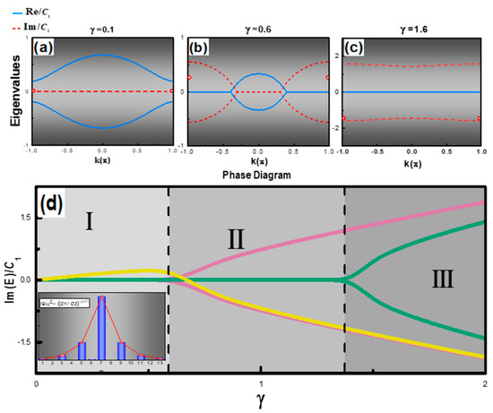
Figure 3.
Complex eigenvalue diagrams of the SSH laser chain system in phase I (a), II (b), and III (c), and red circles denote imaginary parts of the topological zero state. (d) Phase diagram of the complex SSH chain, the yellow curve (color online) represents the topological mode, pink and green curves show the representative bulk modes in the system. The inset shows the topological mode profile calculated at γ = 0.1, along with the theoretical profile ∝(t1/t2)−|n| (red curve).
2.3. Complex Eigenvalue Diagrams of Non-Hermitian Topological Laser Chain
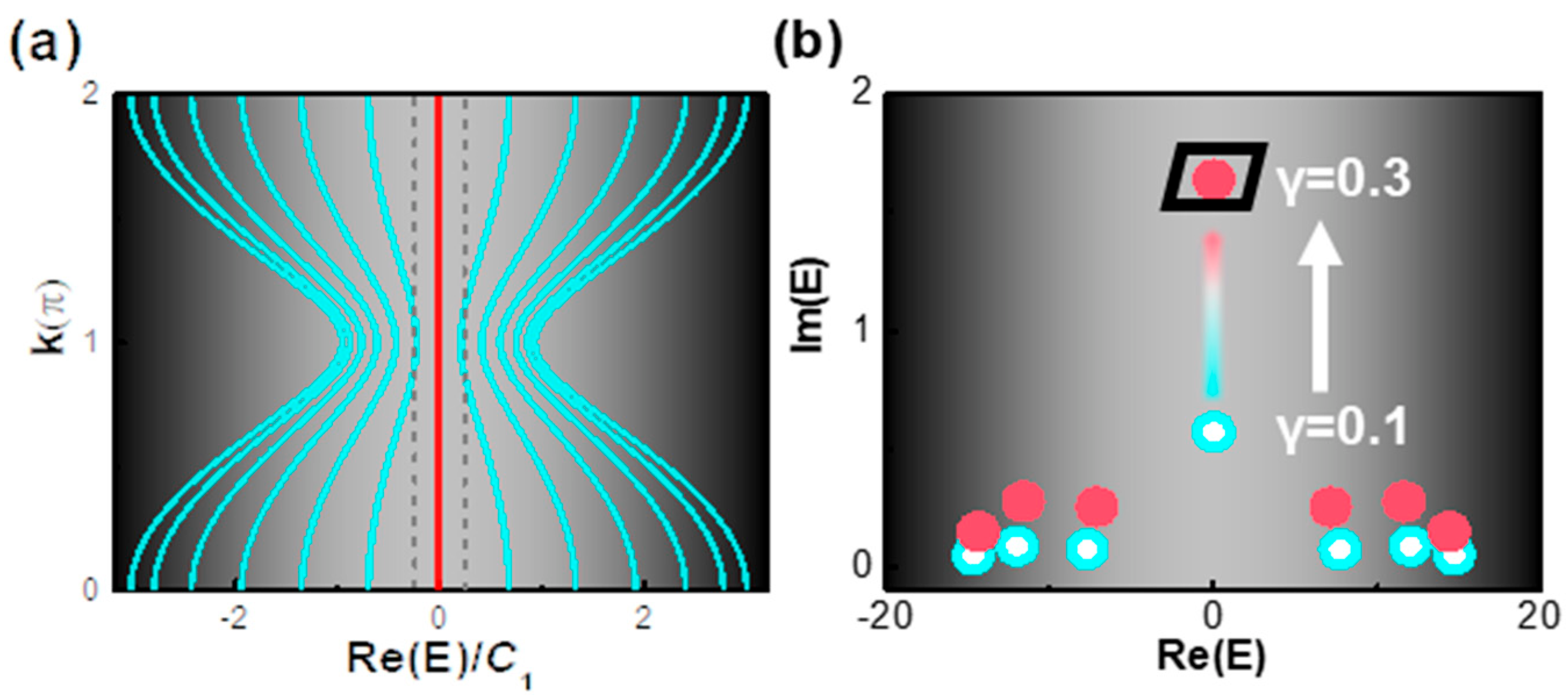
To further investigate the difference between nontrivial zero modes and trivial modes, a complex band diagram in a complex system was calculated. Figure 4a plots the band diagram of the topological system with neither a gain nor a loss. A bandgap was present in the center (between the grey dashed lines), and the topologically protected midgap states (red) sat in the center of the bandgap. Figure 4b shows the dynamic evolution of complex eigenvalues with the γ varying from 0.1 (blue dots) to 0.3 (red dots). With the same bias level, the topological zero states presented a higher gain than other bulk states. As the bias level of the whole system increased evenly, the increment of the topological mode was ~10-times of the ones of trivial modes.

Figure 4.
(a) Band diagram of SSH chain with neither gain nor loss: a bandgap presents clearly between two gray dashed lines, where the midgap states (red) sit in between. (b) Evolution of complex eigenvalues with the γ varied from 0.1 (blue dots) to 0.3 (red dots): the gain increment of the topological zero-mode was ~10 times of the ones of trivial modes (with nonzero real eigenvalue) as the gain level increased.
3. Experimental Results
3.1. Experimental Demonstration of Non-Hermitian Topological Laser Chain
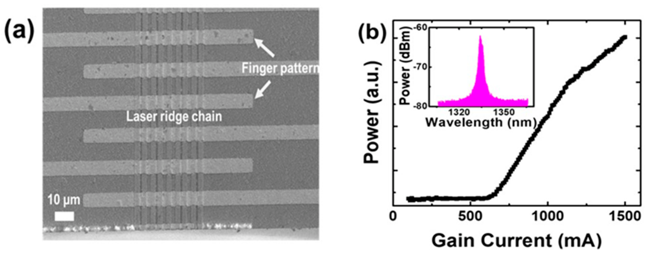
For the experimental demonstration, a topological SSH laser chain was fabricated by standard microfabrication techniques, where the coupling strength, C1 and C2, in the SSH was determined by the trench between each waveguide (see the Materials and Methods the section). The trench width of 1 and 3 µm was employed to define the coupling strength between waveguides C1,and C2. Figure 5a shows the top-view scanning electron microscope (SEM) image of the fabricated laser device, where the finger patterns provided independently controlled gain and loss laser waveguides. The isolation trenches not only controlled the coupling strength, but also provided electrical isolation between each waveguide. The gain/loss SSH chain was operated by electrically biasing the gain and loss waveguides at different levels. The bias current of the loss waveguides was maintained at 0 mA, which corresponded to a loss of ~ 35 cm−1 in the loss waveguide, and the gain waveguide bias current varied from 0 to 1000 mA to electrically tune the gain in the gain waveguides. Figure 5b shows the light–current (L–I) characteristic of the SSH-coupled waveguide laser chain. It was observed that the lasing threshold current was ~600 mA. The inset shows the electroluminescence (EL) spectrum of the laser chain. The lasing wavelength was at ~1.33 µm, and the relative broader laser linewidth was due to the lasing from multiple longitudinal modes in the Fabry–Perot laser cavities.

Figure 5.
Top-view SEM image (a) and light–current (L–I) characteristic (b) of the SSH laser chain. It was observed that the lasing threshold current was ~600 mA. Inset: electroluminescence (EL) spectrum of the laser chain. The lasing wavelength was at 1.33 µm.
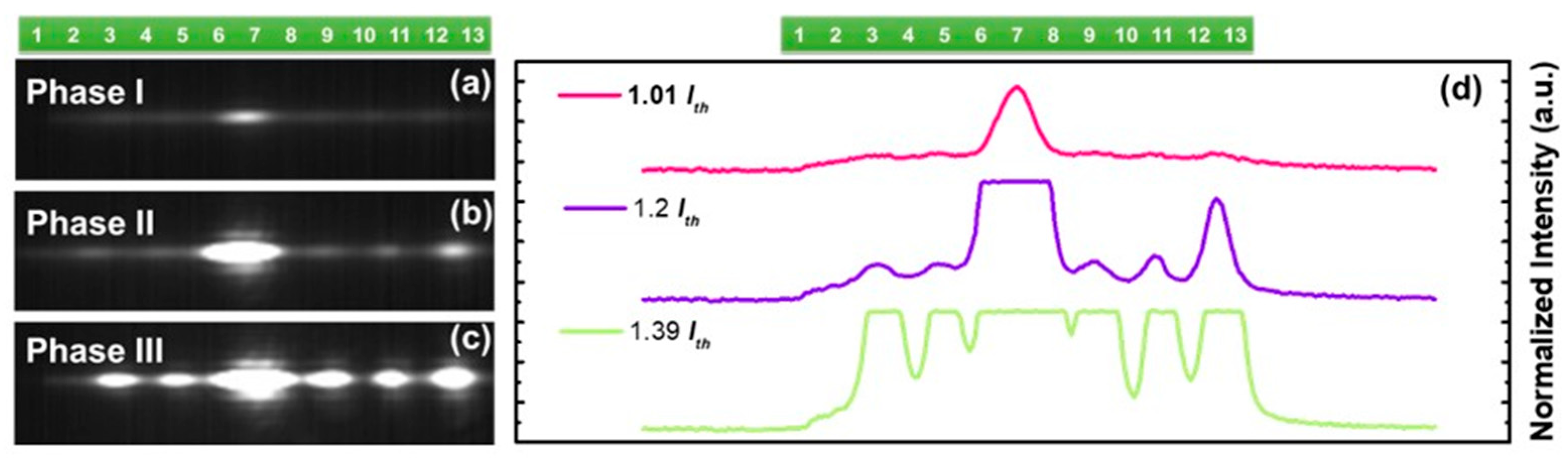
The near-field pattern of the SSH laser chain was measured to investigate the dynamics of the topological mode lasing and mode selections. As shown in Figure 6a–c, the near-field patterns from the laser chain were measured at various gain bias currents. Figure 6d shows the intensity line scans of the near-field images. The intensity saturation was due to the limited dynamic range of the near-infrared (NIR) camera. When the gain bias current was small, 630 mA, the SSH laser chain only lased at the topological mode in the center defect and the mode profile exhibited the maximum intensity at the center defect. When the bias current was increased to 700 mA, the first trivial bulk mode obtained enough gain and transits to the lasing mode, while the topological mode was still dominating in the near-field profile. The SSH laser system evolved to phase II. With a further increment of the bias current to 770 mA, more trivial bulk modes started to obtain enough gain and, eventually, transformed to lasing modes (see Supplementary Materials), which led to a more uniform near-field profile across the laser chain, and the system transited into phase III. The experimental observation showed clear phase transitions of the topological mode laser and agreed well with the theoretical predictions, as shown in Figure 3d. The mode evolution ceased in phase III due to the gain clamping, whereas the output power increased with the increased injection current, as shown in L–I (Figure 5b). It is worth discussing here, that unlike an oddly localized mode profile on the odd site with a small gain in phase I, there were even sites in the order of sixth, fourth, and second, presenting a mode distribution with a larger gain. This was the result of the PT symmetry breaking of bulk modes, and the coupling between nearby sites with the same gains of a sixth and seventh defect waveguide would also suppress the single-mode laser performance. From that perspective, in future work, it is tentative to apply electrical pumping with space symmetry, which adds gain on odd sites and loss on even sites. In that case, the optical mode would maintain localization on odd sites while the gain increased.
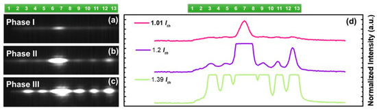
Figure 6.
Near-field patterns measured at varied gain bias currents: (a–c) bias current was 630 mA, 700 mA, and 730 mA. (d) The corresponding intensity line scans to the different bias currents.
3.2. Reconfiguration of Non-Hermitian Topological Laser Chain
The reconfigurability of this topological SSH laser chain was also investigated by replacing the gain defect with a lossy defect. In the experiment, owing to the versatility of the invented electrically injected system, the lossy topological defect was simply achieved by interchanging the gain and loss waveguide bias conditions. The resulting Hamiltonian in the new configuration was equivalent to applying the time-reversal operator to the Hamiltonian of the original system. This new configuration still featured the same topological configuration as in the case discussed before, but now with a lossy defect at the topological interface. The corresponding dispersion relations and phase diagram showed that the topological mode exhibited net loss at a small gain and lasing was prohibited in phase I (see Supplementary Materials). With the increment of the system gain level, both the topological and bulk modes started to obtain a gain, and the lasing of topological and bulk modes occurred in phase II. Figure 7a shows the lasing optical field distribution of the topological mode and bulk mode with a lossy defect system at |γ|=1.2. It is worth noting that at a higher gain, unlike in the previous configuration, the topological mode profile exhibited minimums at the center defect waveguide sites. It could be seen from the topological mode profile evolution at different gain levels (see Supplementary Materials). The lossy topological configuration was also demonstrated experimentally, and the corresponding near-field patterns were measured. As shown in Figure 7b, instead of lasing at a single topological mode, both topological and bulk modes lased at the same time, and the measured near-field pattern represented the superposition of these modes (see Supplementary Materials). The near-field pattern of the original gain defect topological laser at a higher gain was shown to illustrate the relative position of each site as well. The lasing threshold current of the lossy topological defect configuration was ~700 mA, obtained from the L–I measurement. The higher lasing threshold compared to the gain defect topological laser was due to the fact that the lasing could only occur at phase II instead of phase I in this case.
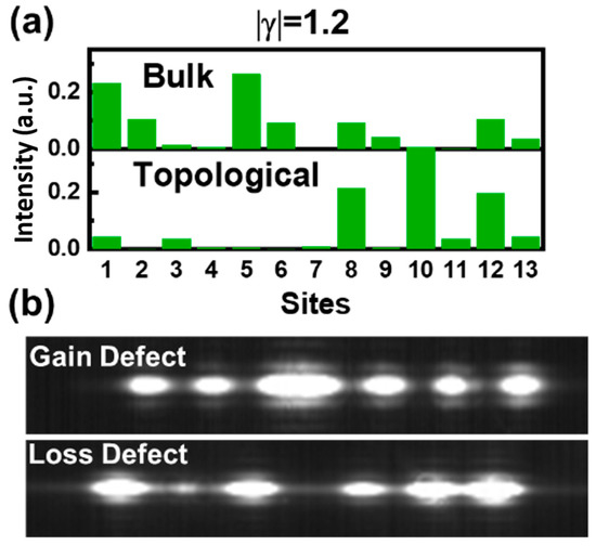
Figure 7.
(a) The optical field intensity distribution of bulk mode and topological mode in configuration with lossy defect, where normalized lossy value was given as |γ| = g/C1 = 1.2; (b) near-field characteristics of the gain and lossy defected topological lasers.
3.3. Topological Laser Chain Fabrication
The QD laser heterostructure was grown on a Si-doped GaAs (100) substrate by a Veeco Gen-II Molecular Beam Epitaxy (MBE) system. The waveguide core and cladding layers of the QD laser heterostructures consisted of GaAs and Al0.4Ga0.6As, with a thickness of 300 nm and 1.5 µm, respectively. In the active region, there were seven layers of InAs quantum dot gain materials with a height of ~5 nm. The QD layers were separated by a 30 nm GaAs spacer layer. The QD laser waveguide was designed at ~1.3 µm.
The topological SSH laser chain was fabricated by standard microfabrication techniques. An AS200 stepper aligner was used to define the ridge width of 3 µm, an isolation trench gap width of 1 and 2 µm, and the fabrication was followed by a dry etching step by the Oxford ICP 380 plasma etcher. The ridge dry etching was stopped at the p-type Al0.4Ga0.6As cladding layer, 200 nm above the top InAs QD layer in the active region. The trench isolation was precisely controlled to provide electrical isolation while yielding coupling strength, C1, and C2, in the dimers. Finally, two finger patterns on the gain and loss waveguides were deposited through the SiNx passivation layer and via holes. The finger patterns provided the simultaneous control of all the gain and loss waveguides electrically, indicating a fast tuning/reconfiguration speed and programmable response. The schematic of the fabricated device is shown in the Supplementary Materials. In total, 24 laser arrays were fabricated on ~ 1x1 cm2 epitaxial wafers, and over 90% of the laser bars exhibited lasing. Among all the lasing devices, similar topological phase transitions were observed.
3.4. Near-Field Measurement
The near-field patterns of the SSH laser chain were measured. The emission from the SSH laser chain was focused by a x100 Mitutoyo NIR objectives lens and the pattern was captured by an Alpha NIR camera through a Mitutoyo FS-70 standard microscope body. The eye-pieces of the microscope and external illumination were used to align the objective with laser facets (see Supplementary Materials).
4. Conclusions
We demonstrated an electrically injected topological laser in an SSH chain with an active gain defect. The theoretical study of the SSH chain was conducted, and phase transitions between the lasing of topological and bulk modes were observed. The lasing of the proposed topological laser system was experimentally demonstrated with a lasing threshold of ~600 mA. The reconfiguration of the system with a lossy defect topological laser was also investigated. Regarding the reconfigurability of the topological SSH chain, the lossy topological defect configuration served as a potential novel platform for applications, such as optical modulators and detectors, where the enhanced absorption was beneficial. Moreover, symmetric biasing on the configurations should be considered in future works.
Supplementary Materials
The following are available online at https://www.mdpi.com/article/10.3390/opt3020013/s1, Figure S1: Topological defect mode profiles at different gain levels with γ varied from 1 to 51 10, Figure S2: Normalized intensity distribution of dominant bulk modes calculated at γ=1.6, 64 where all eigenmodes enter phase III, and possess imaginary eigenenergies, Figure S3: (a) schematics of the SSH laser after the gain and loss waveguides are inter-81 changed, where the original configuration is shown for comparison; (b) phase diagram of 82 the complex SSH chain with loss topological defect and the topological mode possesses 83 loss in Phase I, Figure S4: Schematics of the top (a), cross-section view (b) and oblique-view SEM image (c) 86 of the fabricated device, Figure S5: Schematics of the near-field measurements
Author Contributions
Conceptualization, H.L., R.Y., H.Z. and W.G.; methodology, H.L. and R.Y.; software, H.L., B.Z., S.A., M.H., J.D. and R.Y.; validation, H.L., R.Y. and C.-S.L.; formal analysis, H.L., B.Z., S.A., J.D. and R.Y; investigation, H.L. and R.Y.; resources, R.Y. and C.-S.L.; data curation, H.L.; writing—original draft preparation, H.L. and R.Y.; writing—review and editing, H.L., R.Y., B.Z., S.A., J.D., M.H., H.Z. and W.G.; visualization, H.L., R.Y. and M.H.; supervision, H.Z. and W.G.; project administration, W.G.; funding acquisition, H.Z. and W.G. All authors have read and agreed to the published version of the manuscript.
Funding
R.Y. and W.G. acknowledge funding support from the Massachusetts Clean Energy program. H.L., B.Z., S.A., M.H. and H.Z. gratefully thank funding support provided by the NSF under award CMMI-1661749.
Acknowledgments
The authors acknowledge fabrication facility support by the Harvard University Center for Nanoscale Systems funded by the National Science Foundation under award 0335765.
Conflicts of Interest
The authors declare no conflict of interest.
References
- Qi, X.-L.; Hughes, T.; Zhang, S.-C. Topological field theory of time-reversal invariant insulators. Phys. Rev. B 2008, 78, 195424. [Google Scholar] [CrossRef] [Green Version]
- Fu, L.; Kane, C.L. Topological insulators with inversion symmetry. Phys. Rev. B 2007, 76, 045302. [Google Scholar] [CrossRef] [Green Version]
- Köenig, M.; Wiedmann, S.; Brüene, C.; Roth, A.; Buhmann, H.; Molenkamp, L.W.; Qi, X.-L.; Zhang, S.-C. Quantum Spin Hall Insulator State in HgTe Quantum Wells. Science 2007, 318, 766–770. [Google Scholar] [CrossRef] [PubMed] [Green Version]
- Hsieh, D.; Qian, D.; Wray, L.; Xia, Y.; Hor, Y.S.; Cava, R.J.; Hasan, M.Z. A topological Dirac insulator in a quantum spin Hall phase. Nature 2008, 452, 970–974. [Google Scholar] [CrossRef] [PubMed] [Green Version]
- Hasan, M.Z.; Kane, C.L. Colloquium: Topological insulators. Rev. Mod. Phys. 2010, 82, 3045–3067. [Google Scholar] [CrossRef] [Green Version]
- Hsieh, D.; Xia, Y.; Qian, D.; Wray, L.; Meier, F.; Dil, J.H.; Osterwalder, J.; Patthey, L.; Fedorov, A.V.; Lin, H.; et al. Observation of Time-Reversal-Protected Single-Dirac-Cone Topological-Insulator States in Bi2Te3 and Se2Te3. Phys. Rev. Lett. 2009, 103, 146401. [Google Scholar] [CrossRef] [Green Version]
- Qi, X.-L.; Zhang, S.-C. The quantum spin Hall effect and topological insulators. Phys. Today 2009, 63, 33–38. [Google Scholar] [CrossRef] [Green Version]
- Qi, X.-L.; Zhang, S.-C. Topological insulators and superconductors. Rev. Mod. Phys. 2011, 83, 1057–1110. [Google Scholar] [CrossRef] [Green Version]
- Fu, L.; Kane, C.L. Superconducting Proximity Effect and Majorana Fermions at the Surface of a Topological Insulator. Phys. Rev. Lett. 2008, 100, 096407. [Google Scholar] [CrossRef] [Green Version]
- Poli, C.; Bellec, M.; Kuhl, U.; Mortessagne, F.; Schomerus, H. Selective enhancement of topologically induced interface states in a dielectric resonator chain. Nat. Commun. 2015, 6, 6710. [Google Scholar] [CrossRef] [Green Version]
- Rechtsman, M.C.; Zeuner, J.M.; Plotnik, Y.; Lumer, Y.; Podolsky, D.; Dreisow, F.; Nolte, S.; Segev, M.; Szameit, A. Photonic Floquet topological insulators. Nature 2013, 496, 196–200. [Google Scholar] [CrossRef] [PubMed]
- Umucalılar, R.O.; Carusotto, I. Artificial gauge field for photons in coupled cavity arrays. Phys. Rev. A 2011, 84, 043804. [Google Scholar] [CrossRef] [Green Version]
- Hafezi, M.; Demler, E.A.; Lukin, M.D.; Taylor, J.M. Robust optical delay lines with topological protection. Nat. Phys. 2011, 7, 907–912. [Google Scholar] [CrossRef]
- Fang, K.; Yu, Z.; Fan, S. Realizing effective magnetic field for photons by controlling the phase of dynamic modulation. Nat. Photon. 2012, 6, 782–787. [Google Scholar] [CrossRef]
- Hafezi, M.; Mittal, S.; Fan, J.; Migdall, A.; Taylor, J.M. Imaging topological edge states in silicon photonics. Nat. Photon. 2013, 7, 1001–1005. [Google Scholar] [CrossRef] [Green Version]
- Cheng, X.; Jouvaud, C.; Ni, X.; Mousavi, S.H.; Genack, A.Z.; Khanikaev, A.B. Robust reconfigurable electromagnetic pathways within a photonic topological insulator. Nat. Mater. 2016, 15, 542–548. [Google Scholar] [CrossRef]
- Lu, L.; Joannopoulos, J.D.; Soljačić, M. Topological photonics. Nat. Photonics 2014, 8, 821. [Google Scholar] [CrossRef] [Green Version]
- Bandres, M.A.; Wittek, S.; Harari, G.; Parto, M.; Ren, J.; Segev, M.; Christodoulides, D.N.; Khajavikhan, M. Topological insulator laser: Experiments. Science 2018, 359, eaar4005. [Google Scholar] [CrossRef] [Green Version]
- Parto, M.; Wittek, S.; Hodaei, H.; Harari, G.; Bandres, M.A.; Ren, J.; Rechtsman, M.C.; Segev, M.; Christodoulides, D.N.; Khajavikhan, M. Complex edge—State phase transitions in 1D topological laser arrays. arXiv preprint 2017, arXiv:1709.00523. [Google Scholar]
- Zhao, H.; Miao, P.; Teimourpour, M.H.; Malzard, S.; El-Ganainy, R.; Schomerus, H.; Feng, L. Topological hybrid silicon microlasers. Nat. Commun. 2018, 9, 981. [Google Scholar] [CrossRef]
- St-Jean, P.; Goblot, V.; Galopin, E.; Lemaître, A.; Ozawa, T.; Le Gratiet, L.; Sagnes, I.; Bloch, J.; Amo, A. Lasing in topological edge states of a one-dimensional lattice. Nat. Photonics 2017, 11, 651–656. [Google Scholar] [CrossRef] [Green Version]
- Parto, M.; Wittek, S.; Hodaei, H.; Harari, G.; Bandres, M.A.; Ren, J.; Rechtsman, M.C.; Segev, M.; Christodoulides, D.N.; Khajavikhan, M. Edge-Mode Lasing in 1D Topological Active Arrays. Phys. Rev. Lett. 2018, 120, 113901. [Google Scholar] [CrossRef] [PubMed] [Green Version]
- Bahari, B.; Ndao, A.; Vallini, F.; El Amili, A.; Fainman, Y.; Kanté, B. Nonreciprocal lasing in topological cavities of arbitrary geometries. Science 2017, 358, 636–640. [Google Scholar] [CrossRef] [PubMed] [Green Version]
- Pilozzi, L.; Conti, C. Topological cascade laser for frequency comb generation in PT-symmetric structures. Opt. Lett. 2017, 42, 5174–5177. [Google Scholar] [CrossRef] [Green Version]
- Longhi, S. Non-Hermitian Gauged Topological Laser Arrays. Ann. Phys. 2018, 530, 1800023. [Google Scholar] [CrossRef] [Green Version]
- Wu, Y.; Li, C.; Hu, X.; Ao, Y.; Zhao, Y.; Gong, Q. Applications of Topological Photonics in Integrated Photonic Devices. Adv. Opt. Mater. 2017, 5, 1700357. [Google Scholar] [CrossRef]
- Rüter, C.E.; Makris, K.G.; El-Ganainy, R.; Christodoulides, D.N.; Segev, M.; Kip, D. Observation of parity-time symmetry in optics. Nat. Phys. 2010, 6, 192. [Google Scholar] [CrossRef] [Green Version]
- Guo, A.; Salamo, G.; Duchesne, D.; Morandotti, R.; Volatier-Ravat, M.; Aimez, V.; Siviloglou, G.; Christodoulides, D. Observation of P T-symmetry breaking in complex optical potentials. Phys. Rev. Lett. 2009, 103, 093902. [Google Scholar] [CrossRef] [Green Version]
- El-Ganainy, R.; Makris, K.G.; Christodoulides, D.N.; Musslimani, Z.H. Theory of coupled optical PT-symmetric structures. Opt. Lett. 2007, 32, 2632–2634. [Google Scholar] [CrossRef]
- Feng, L.; Ayache, M.; Huang, J.; Xu, Y.-L.; Lu, M.-H.; Chen, Y.-F.; Fainman, Y.; Scherer, A. Nonreciprocal Light Propagation in a Silicon Photonic Circuit. Science 2011, 333, 729–733. [Google Scholar] [CrossRef] [Green Version]
- Peng, B.; Özdemir, Ş.K.; Lei, F.; Monifi, F.; Gianfreda, M.; Long, G.L.; Fan, S.; Nori, F.; Bender, C.M.; Yang, L. Parity-time-symmetric whispering-gallery microcavities. Nat. Phys. 2014, 10, 394–398. [Google Scholar] [CrossRef] [Green Version]
- Feng, L.; Wong, Z.J.; Ma, R.-M.; Wang, Y.; Zhang, X. Single-mode laser by parity-time symmetry breaking. Science 2014, 346, 972–975. [Google Scholar] [CrossRef] [PubMed]
- Chong, Y.; Ge, L.; Stone, A.D. P T-Symmetry Breaking and Laser-Absorber Modes in Optical Scattering Systems. Phys. Rev. Lett. 2011, 106, 093902. [Google Scholar] [CrossRef] [PubMed] [Green Version]
- Hodaei, H.; Miri, M.-A.; Heinrich, M.; Christodoulides, D.N.; Khajavikhan, M. Parity-time-symmetric microring lasers. Science 2014, 346, 975–978. [Google Scholar] [CrossRef]
- Su, W.P.; Schrieffer, J.; Heeger, A.J. Solitons in polyacetylene. Phys. Rev. Lett. 1979, 42, 1698. [Google Scholar] [CrossRef]
- Malkova, N.; Hromada, I.; Wang, X.; Bryant, G.; Chen, Z. Observation of optical Shockley-like surface states in photonic superlattices. Opt. Lett. 2009, 34, 1633–1635. [Google Scholar] [CrossRef]
- Delplace, P.; Ullmo, D.; Montambaux, G. Zak phase and the existence of edge states in graphene. Phys. Rev. B 2011, 84, 195452. [Google Scholar] [CrossRef] [Green Version]
- Zak, J. Berry’s phase for energy bands in solids. Phys. Rev. Lett. 1989, 62, 2747. [Google Scholar] [CrossRef]
- Bender, C.M.; DeKieviet, M.; Klevansky, S.P. PT quantum mechanics. Philos. Trans. A Math. Phys. Eng. Sci. 2013, 371, 20120523. [Google Scholar] [CrossRef] [Green Version]
- Weimann, S.; Kremer, M.; Plotnik, Y.; Lumer, Y.; Nolte, S.; Makris, K.G.; Segev, Y.P.Y.L.M.; Rechtsman, M.C.; Szameit, A. Topologically protected bound states in photonic parity-time-symmetric crystals. Nat. Mater. 2016, 16, 433–438. [Google Scholar] [CrossRef]
- Yuce, C. Topological phase in a non-Hermitian PT symmetric system. Phys. Lett. A 2015, 379, 1213–1218. [Google Scholar] [CrossRef] [Green Version]
- Coldren, L.A.; Corzine, S.W.; Mašanović, M.L. Diode Lasers and Photonic Integrated Circuits; John Wiley & Sons: Hoboken, NJ, USA, 2012. [Google Scholar]

Publisher’s Note: MDPI stays neutral with regard to jurisdictional claims in published maps and institutional affiliations. |
© 2022 by the authors. Licensee MDPI, Basel, Switzerland. This article is an open access article distributed under the terms and conditions of the Creative Commons Attribution (CC BY) license (https://creativecommons.org/licenses/by/4.0/).