Abstract
Resistance spot welding of aluminum alloys causes the electrode materials to degrade rapidly. This is due to diffusion processes occurring between the sheet materials and the copper electrodes at process temperatures of up to 600 °C. This significantly limits the electrode life, resulting in less than 60 weld cycles before the joint quality becomes insufficient. Thin-film diffusion barriers can increase electrode life and improve joint quality. This article describes the generation of barrier layers of nickel and tungsten using physical vapor deposition. These layers directly influence the welding process by altering the electrical resistance and friction coefficients in the contact area. Nanoindentation is used to determine the specific properties of the barrier layers within the 2.5–3 µm layer thickness range. Hardness and modulus of elasticity are determined by indentation tests. Scratch tests determine the friction coefficients and adhesion strength of the coating against plastic deformation. Nanoindentation is also used to investigate the degradation process of the electrode base material and barrier layers. This reveals which damage mechanisms occur with uncoated electrodes and demonstrates how thin-film diffusion barrier coatings can prevent aluminum diffusion.
Keywords:
resistance spot welding; electrode degradation; CuCr1Zr; diffusion; nanoindentation; SEM; SIMS 1. Introduction
Resistance spot welding is primarily used in car body production due to its high efficiency and short cycle times. Since the 1980s, the proportion of aluminum in vehicles has been steadily increasing [1]. In contrast to steel materials, rapid damage occurs to the electrodes used when welding aluminum. This significantly shortens the electrode life and reduces the cost-effectiveness of the joining process [2]. The resulting damage mechanisms are due to diffusion processes in the Cu-Al system that occur between the electrodes and the sheet materials at high process temperatures.
The electrode life is determined within welding experiments. When the joint quality falls below a certain quality criterion, the electrode life is exceeded. A quality criterion can be defined as falling below a defined weld diameter, the formation of weld spatter, or sticking between the electrode and the sheet material. A decrease in joint quality is caused by the increasing degradation of the electrodes. With the first weld, aluminum adheres to the electrode surfaces. The continuous diffusion creates various intermetallic phases in the Cu-Al system. As the intermetallic phases grow, pitting occurs, causing parts of the affected material area to break off and form cavities on the surface [2,3,4].
The degradation of the electrode material is caused by thermal loads in the welding process, which lead to diffusion in the Cu-Al system. The natural oxide layer on the Al sheets causes high current densities on the electrode surfaces [5]. This results in locally high temperatures and accelerated diffusion processes. The chemical, thermal, and mechanical changes in the electrode material cause continuous damage to the material areas [5,6]. The result is welded joints with decreasing joint quality and reduced weld spot diameters [7]. To date, various approaches have been investigated to reduce the damage mechanisms and extend the electrode life.
In general, the usage of high electrode forces in combination with short welding times is a fundamental requirement for achieving the desired results [8]. In addition, weld lens formation and electrode service life depend on the condition of the sheet metal surface and the thickness of the oxide layer. Pre-treatment techniques, such as chemical or mechanical oxide removal or surface passivation, offer possibilities to reduce electrode degradation [9,10,11]. On the other hand, the application of certain lubricants between the contact electrode sheet can lead to an increased service life [12]. Alternatively, in Ref. [13], the coating of the sheet materials (AW-6111/core sheet clad with an AW-4040/cover sheet) was tested, with positive results. For the process-integrated dissolution of oxide layers, superimposed electrode movement can also be used (e.g., by rotating the electrodes around the longitudinal axis or by performing a rolling motion in relation to the sheet plane) [14,15].
To deliberately destroy the oxide layer on the aluminum sheets, the surfaces of the electrodes can also be textured [16,17,18]. The approaches chosen range from microstructuring using lasers, sandblasting, or machining-based macrostructuring. The application of asymmetrical structuring (in relation to the anode and cathode sides) can also be effective [19]. The service life of the electrodes can also be influenced by varying their chemical composition. In [20], it was shown that the tendency of electrodes to stick can be reduced by adding Ag due to the higher electrical conductivity. In the DeltaSpot process (Fa. Fronius), nickel strips are fed between the electrodes and the sheet materials. This avoids direct Cu-Al contact, which can prevent diffusion processes [21]. Although the electrode’s life can be significantly increased, a modification of the welding gun is necessary. Other approaches pursue the modification of the electrodes by generating diffusion barriers. Various sources are known in which the materials and the thickness of the diffusion barriers applied to copper-based electrodes differ. Electrospark deposition can be used to generate composite coating barriers in the layer thickness range of 30–100 µm [22,23,24,25]. Systems are from the types of TiC, TiB2-TiC, ZrB2-TiB2, and Al203-TiB2—the last one with and without a Ni-buffer layer. In the case of metallic coatings (using electroplating), studies exist for the materials Fe, Co, Cr, and Ni [26]. The best results were achieved with Ni layers with thicknesses of 5 µm. Studies on thinner diffusion barriers <3 µm (using physical vapor deposition) for the materials Ni, W, and TiB2 have already been published [18].
In the previous work, the achievable increase in electrode life and the positive effects on the welding process made possible by diffusion barriers were investigated. However, to the present date, there are no publications that describe the existing properties of the degradation area or explain the exact characteristics of the diffusion barriers. It is, therefore, necessary to investigate the interactions between the degradation of the electrode base material and the generated diffusion barriers in a more detailed manner. The selected investigation methods include EDX (energy dispersive X-ray spectroscopy) and SIMS (secondary ion mass spectrometry) analyses, which allow the elemental composition and diffusion depth to be determined. Nanoindentation is also used to provide a detailed picture of the mechanical properties of the degraded area of the CuCr1Zr electrodes.
In the nanoindentation analysis, low test forces are required to determine the coating properties, especially for thin coatings or phase seams. Higher test forces lead to measurement inaccuracies, which can be influenced by the substrate material or nearby phases [27]. The maximum penetration depth of the indenter tip should, therefore, not exceed 10–20% of the coating or phase thickness [28]. Nanoindentation can be used to investigate electrode degradation and the diffusion barriers that are generated. Local measurements enable the determination of the coating hardness and the modulus of elasticity. Scratch tests are based on lateral movement and are suitable for determining the coefficient of friction. In addition, the adhesion properties of a coating can be determined, whereby a test can be carried out under both constant and continuously increasing loads [28,29]. However, it must be noted that soft substrate materials have a greater tendency to plasticize during the scratch test. A scratch test under almost elastic conditions should, therefore, be limited to a penetration depth <10% of the coating thickness [30].
In this study, the degradation of electrodes during resistance spot welding of the alloy AlMg3 is investigated. For this purpose, the degraded regions of the electrodes are examined by means of nanoindentation, SEM, EDX, and SIMS with regard to the resulting phase seams. In this way, the mechanisms of degradation, including pitting, can be described in detail. Thin-film diffusion barriers of the materials Ni (3.0 µm) and W (2.5 µm) are generated on electrodes by means of PVD (physical vapor deposition). The influence of the diffusion barriers on the welding process is investigated by means of electrode life tests. Furthermore, the mechanical properties of the coatings and their resistance to diffusion are demonstrated.
2. Materials and Methods
Electrodes with the material CuCr1Zr (Cu with 1 wt.% Cr and traces of Zr) and the geometry ISO 5821 A0-20-22-100 were used in the investigations. The thin-film diffusion barriers were generated by physical vapor deposition (CC800-9 Custom, Cemecon, Aachen, Germany). A field emission scanning electron microscope (Helios Nanolab 600, FEI/Thermofisher, Hillsboro, OR, USA) was used to determine the generated coating thicknesses and the coating morphology. The degradation states of the electrodes used were generated within welding experiments using a resistance spot welding gun(PowerGun2, Nimak, Wissen, Germany). The properties of the generated coatings and the phases of degraded areas were investigated a nanoindentation device (Hysitron TI Premier II, Bruker, Wissembourg, France). Local testing was carried out using a Berkovich indenter, while scratch tests were performed using a radial indenter with a diameter of 5 µm.
Isothermal diffusion annealing at 600 °C was done using a rapid thermal annealing setup (20 K/s). Secondary ion mass spectrometry (SIMS) measurements were carried out with a machine type (IMS-3f, Cameca, Gennevilliers, France) in the depth profile mode and a double-focusing mass spectrometer with a primary O2− ion beam at 15 keV and 50–150 nA. Depth calibration was done with a profilometer (AlphaStep 500, KLA-Tecnor, Milpitas, CA, USA).
3. Results and Discussion
3.1. Resistance Spot Welding—Electrode Degradation
Within the welding experiments, two sheets of AlMg3 (Al with 3 wt.% Mg) material with a single sheet thickness of 1 mm were joined by using the welding parameters in Table 1, resulting in a weld diameter of 5 mm. This diameter complies with the standard requirements for spot welding of 5∙√t (t: sheet thickness in mm) of the international standards AWS D8.2M and ISO 18595. The weld diameter is determined by means of a chisel test. Every tenth weld is also examined by metallographic microsection.
Table 1.
Parameter set for standard electrodes—AlMg3 (2 × 1 mm).
A total of three test runs were carried out, each with new electrode pairs. During the welding experiments, the surfaces of the joints were examined for imperfections that described the defined stages of degradation. These include melting of the sheet surface, cracking of the sheet surface, the formation of weld spatter, and sticking between the electrode and the sheet surface. The electrode life ends when sticking occurs. The sticking between the electrode and the sheet is caused by chemical melting of both elements. It can be assumed that the sticking effect leads to significant damage to the electrodes and, therefore, the electrode life ends at this criterion. The worst case scenario (earliest occurrence) from the three test runs was evaluated (Table 2).
Table 2.
Welding experiments—quantity of welds until the occurrence of imperfections.
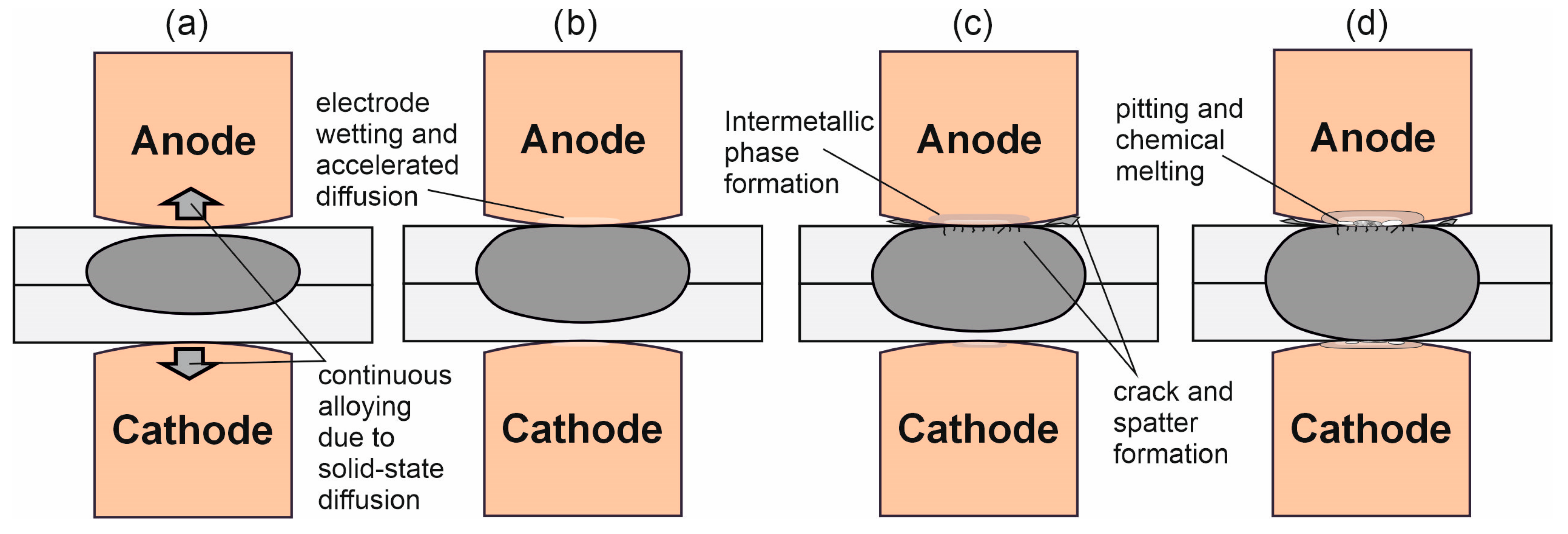
Resistance spot welding of the alloy AlMg3 led to a decrease in joint quality after only a few welds—the melting of the sheet surface results in contact between a molten Al phase and the Cu electrode. The diffusion rate of the Cu atoms into the molten Al phase is about five times higher than the diffusion rate of Al atoms into the solid Cu phase [31]. Therefore, the second weld within the welding experiments already leads to a chemical melting of the electrode surface. Since the molten aluminum is no longer stabilized by a solid phase, the probability of surface cracks (8th weld) and the formation of weld spatter (26th weld) increases. When the electrode surface comes into contact with the molten aluminum over a large area, a material bond is formed between the two objects. At the end of the welding process, this material bond is mechanically destroyed, which significantly reduces the quality of the joint. The electrode life, therefore, ends with the electrode sticking (58th weld). The different stages of electrode degradation are shown in Figure 1.
Figure 1.
Different stages of electrode degradation: Initial state → continuous alloying of the electrodes/displacement of the weld lens in the anode direction due to the Peltier effect (a); increase in contact resistance → enlargement of the welding lens/melting of the sheet metal surface and wetting of the electrode surface with Al; (b) intermetallic phase formation → crack and spatter formation as a result of further increased contact resistance; (c) expansion of intermetallic phase formation, chemical melting, pitting and finally adhesion of the electrode at the sheet surface (d).
The degradation of the electrode working surfaces due to diffusion processes can be caused by solid-state diffusion or chemical melting. As chemical melting greatly accelerates the degradation of the electrode surface, there is a direct dependence on the process temperature occurring in the Cu-Al contact. Tactile measurement of the process temperature is not possible due to the high currents. There is insufficient accessibility to the contact area for optical temperature measurement. A temperature measurement in the half-section test was unsuccessful due to the low result density. Therefore, the maximum temperature in the welding process was approximated by a metallographic microsection of a spot-welded joint (Figure 2).
Figure 2.
Metallographic microsection of a spot-welded joint, AlMg3 (a), and binary Al-Mg phase diagram (b) that is based on [32].
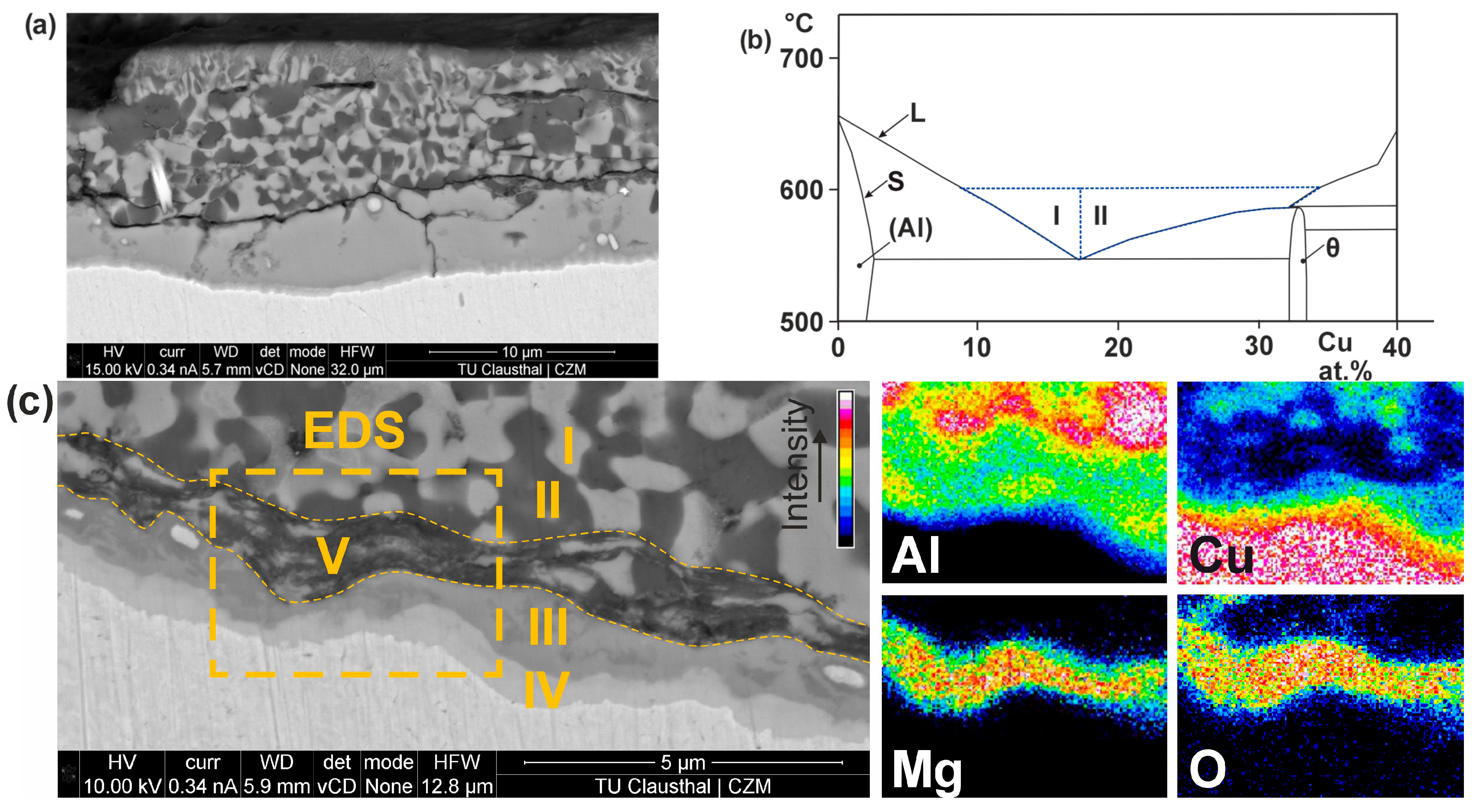
The solidus (S) and liquidus (L) temperature ranges are visible in the metallographic microsection. Based on the binary Al-Mg phase diagram, the respective temperature ranges for the alloy AlMg3 (3.3 at.% Mg) are approximately 617 °C (S) and 649 °C (L). When the sheet surface is melted, it can, therefore, be assumed that at least the temperature of the solidus range is present on the sheet surface. Additional information about the occurring process temperatures can be obtained on the basis of a metallographic cross-section of a degraded electrode (Figure 3).
Depending on the temperature, the electrode degrades by solid-state diffusion or chemical melting (Figure 3a). Solid-state diffusion occurs near the unaffected electrode material, CuCr1Zr, at lower temperatures—two intermetallic phases, III and IV, form in this area. Chemical melting takes place at higher temperatures, forming a near-eutectic composition of phases I (Cu-rich phase) and II (Al-rich phase). In this area, the melting temperature of the Cu-Al contact is reduced to approximately 548 °C at maximum (Figure 3b). Due to the brittle properties of the intermetallic phases, the high electrode force causes cracks to form along the phase seam. Fracturing of these material areas leads to pitting in the form of erosion of the electrode working face. An analysis of the individual phases of the degraded material area using EDX allows the chemical compositions to be determined (Figure 3c). Phases I and II vary widely in their composition and, therefore, cannot be precisely determined by EDX analysis. In the intermetallic phases, there is a consistent elemental composition, which can be determined quantitatively by EDX analysis. Due to its composition, the upper phase seam (III; 66.6 at.% Al; 33.4 at.% Cu) can be assigned to the intermetallic Θ-phase, and the lower phase seam (IV; 41.1 at.% Al; 58.8 at.% Cu) to the intermetallic δ-phase. The EDX mapping also shows a local enrichment of Mg and O. It can be assumed that MgO is partially located in the degraded layer due to the low contents. The Θ-phase has a specific electrical resistance of 7.2 µΩcm, and the δ-phase 28.7 µΩcm [34]. Because the intermetallic phases have a 75% (Θ-phase) or 93% (δ-phase) lower specific electrical conductivity compared to Cu, the high current densities cause disproportionate heating of the electrode working faces.
3.2. Analysis of the Electrode Degradation by Nanoindentation
A Berkovich indenter tip and a transducer for measurement data acquisition in normal and lateral directions were used to investigate the degraded material area of the CuCr1Zr electrode. In the first step, a mapping of indentations was used to investigate the hardness and modulus of elasticity of the degraded material area (Figure 4).
Figure 4.
Scanning probe microscopy (SPM) of degraded material area: 2D view (a); isometric view (b).
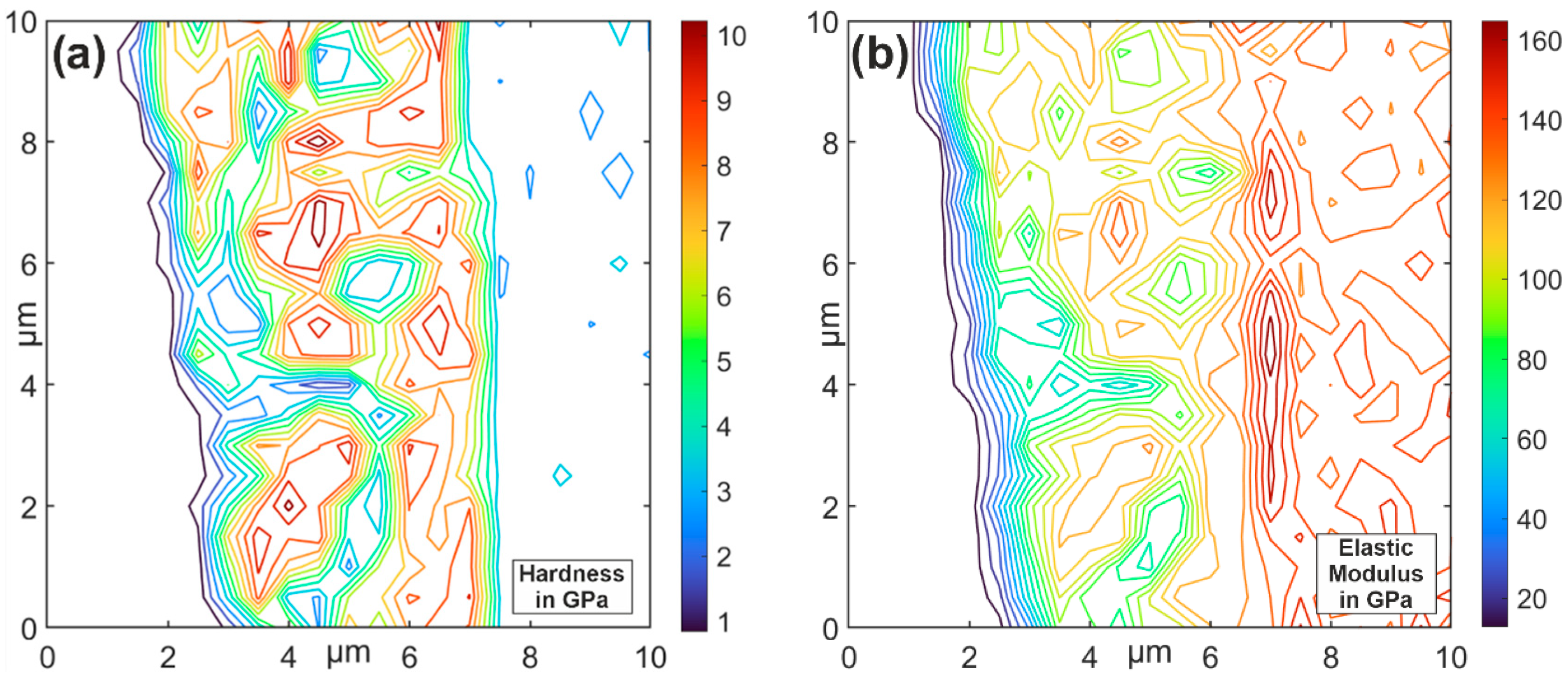
The indenter tip scanned the topography of the material area (scanning probe microscopy—SPM) so that the elevation information can be considered for a subsequent hardness measurement. The load of the indenter tip was 2 µN during SPM scanning (pre- and post-scan). The hardness measurement was performed with an indenter force of 200 µN and a spacing of 500 nm. The left side of the SPM image shows the surrounding polymer of the embedded metallographic sample. Depending on the indentation depth, it can be seen that the adjacent phase on the Cu base material (right-sided) tends to have a homogeneous hardness distribution. In the outer edge area of the degraded electrode (middle), there are more localized areas that show a significantly deeper penetration of the indentation tip. The hardness and modulus of elasticity of the material area are calculated on the basis of the load and unloading curves of the individual indentations (Figure 5).
Figure 5.
Indentation mapping of degraded material area: hardness (a); elastic modulus (b).
The base material, CuCr1Zr, of the electrode has an average hardness of 2.9 GPa and a modulus of elasticity of 135.6 GPa. Based on the SPM scan (Figure 4), the different intermetallic phases cannot be differentiated. In the indentation mapping, the suspected area of the intermetallic δ-phase shows a significant increase in the average hardness of 7.3 GPa and the modulus of elasticity of 158.9 GPa. The intermetallic Θ-phase is suspected in the adjacent series measurement. Here, the average hardness is 8.7 GPa, and the modulus of elasticity is 122.8 GPa. In the central area of the SPM scan, the areas of local increase in penetration depth can be determined. These areas show a significant reduction in the average hardness of 2.6 GPa and modulus of elasticity of 64.6 GPa. The measuring device was calibrated using a standard quartz sample, resulting in a measurement accuracy of 2–3%. An exact assessment of the geometric position of the intermetallic phases is not possible on the basis of the indentation mapping. It is also not possible to determine the local reduction in hardness and modulus of elasticity on the basis of these investigations. For further characterization, the measured region was examined using energy dispersive X-ray spectroscopy (Figure 6).
Figure 6.
Scanning electron microscopy (SEM): overview of the indentation mapping → dotted line: compositions measurements; yellow box: EDX mapping area (a); element composition of the local EDX analysis 1–7 (b); EDX mapping of the material transition area → element intensity ascending according to following colors: black, blue, green, yellow, red (c).
In the area of indentation mapping, the regions of reduced hardness can be recognized by the dark phase regions (Figure 6a). In the illustration, bright phases have elements with a high atomic weight (Cu-rich) and dark phases have elements with a low atomic weight (Al-rich). The characterization of the elemental composition was carried out using an EDX line measurement at seven measuring positions (Figure 6b). The accelerating voltage of the EDX analysis was 5 keV. The material areas with a low hardness are primarily composed of aluminum with a proportion >85% and low proportions of copper (EDX measurements 1–3). The element composition of the δ-phase is present in the solid-state diffusion region (EDX measurement 5 and 6). The measurements along the phase seam were repeated multiple times. This caused slight fluctuations in the results, with the accuracy of the measurements expected to be in the range of ~5%. The Θ-phase cannot be determined by the element composition. This could be explained by the distances between the EDX measurements being too wide or the area of the local intermetallic phase being too thin. The EDX mapping shows that a further intermetallic phase could be present in the material transition (Figure 6c). Due to the thin phase seam, it is not possible to quantify the elements and, thus, provide verification by measurement.
In the material area investigated, the region of solid-state diffusion is relatively thin compared to Figure 3. This results in a more difficult differentiation between the two detected intermetallic phases. An improvement in the results can be achieved by further reducing the measuring distances for nanoindentation and EDX analysis. For nanoindentation, it is also necessary to limit the penetration depth in order to prevent mutual interference between the local measurement positions. Quantitative measurement of the element composition is limited, particularly in the case of thin phase seams, as a further reduction in the acceleration voltage below 5 keV could greatly reduce the result density.
3.3. Thin-Film Diffusion Barriers in Resistance Spot Welding
The use of diffusion barriers on the electrode working faces is intended to prevent direct Cu-Al contact within the welding process. The aim is to prevent aluminum diffusion and the degradation of the electrode material. This is intended to significantly delay the occurrence of imperfections and increase the electrode life. The elements Ni and W are to be investigated as diffusion barriers. The diffusion barriers are produced by physical vapor deposition, whereby a comparable layer thickness of 3.0 µm (Ni) and 2.5 µm (W) was achieved. The diffusion barriers generated should first be examined with regard to their mechanical, electrical, and thermal properties (Table 3).
Table 3.
Properties of the diffusion barriers compared to the base material.
The hardness and modulus of elasticity of the materials are determined by nanoindentation. A Berkovich indenter tip is used at a test load of 2 mN. At this load, a penetration depth of approximately 155 nm occurs in the CuCr1Zr base material. The penetration depth is, therefore, around 5% (Ni) or 6% (W) of the layer thickness of the diffusion barriers. It can, therefore, be assumed that the soft base material has no direct influence on the measurement results of the harder coatings. The results are calculated from the mean value of five measurements. The CuCr1Zr base material has a hardness of 3.7 GPa and a modulus of elasticity of 140.4 GPa. The values deviate from the results in Figure 6. This is due to the higher test load and larger measuring spacing, which prevents the measurements from influencing each other (compared to the spacing used in hardness mapping). The diffusion barrier coatings, on the other hand, have a significantly higher hardness of 6.7 GPa (Ni) and 18.5 GPa (W). The coefficient of friction is determined using a test load of 5 mN and a simultaneous movement in the lateral direction. A radial indenter tip with a tip radius of 5 µm is used to determine the coefficient of friction. The friction coefficient of the CuCr1Zr base material is 0.24. The diffusion barriers reduce the friction coefficient by around 33% (Ni) or 37% (W). The electrical resistance is measured in the static case between two electrodes and one sheet of AlMg3 (1 mm). The test load between the electrodes is 3 kN, and the test current is 10 A (DC). When using the reference electrodes, the electrical resistance is 210 µOhm. Diffusion barriers lead to a significant reduction in electrical resistance of around 74% (Ni) or 60% (W). It is assumed that the dendritic surface structure of the diffusion barriers leads to a penetration of the natural aluminum oxide layer, which significantly improves the electrical conductivity. The thermal conductivity of the materials is determined using laser flash analysis. The samples consist of a 1 mm thick slice of the material CuCr1Zr, which is analyzed in an inert gas atmosphere. It is shown that the use of diffusion barriers leads to a reduction in thermal conductivity. Based on a temperature of 600 °C, there is a reduction of 20% (Ni) or 42% (W).
The diffusion barriers lead to a significant change in the properties of the electrode working faces. Because there is a direct influence on the welding process, it is necessary to adjust the process variables in order to achieve a comparable weld diameter of 5 mm (5∙√t) (Table 4). The electrode life is determined under identical conditions, whereby each test series is carried out twice. For the first occurrence of a defined imperfection, the worst case scenario is applied again (Table 5).
Table 4.
Parameter set for electrodes with thin-film diffusion barrier—AlMg3 (2 × 1 mm).
Table 5.
Welding experiments—quantity of welds until the occurrence of imperfections.
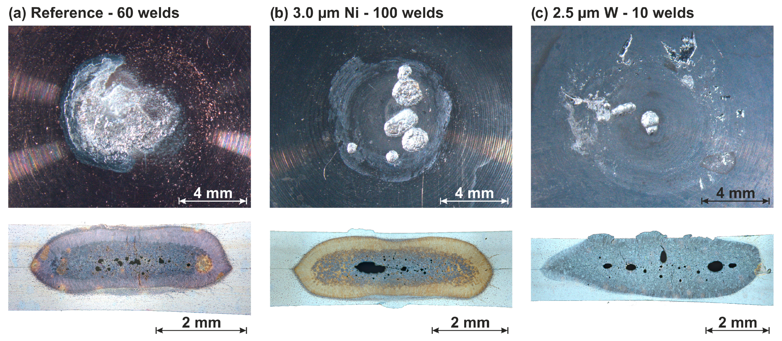
To achieve a weld diameter of 5 mm (5∙√t), the weld current must be increased to 21.1 kA, compared to the uncoated reference electrodes. The diffusion barriers have a dendritic surface structure that contributes to the penetration of the natural oxide layer of the sheet metal materials. This reduces the electrical contact resistance, which requires the weld current to be adjusted. The two diffusion barriers also exhibited contrasting behavior with regard to the initial occurrence of imperfections and the achievable electrode life. Ni led to a significant delay in the occurrence of imperfections. Melting of the sheet surface occurred only after 37 welds, and the first crack formation on the sheet surface occurred after 95 welds. The occurrence of weld spatter was not detected. Electrode sticking was also only detected after 108 welds, which significantly increased the electrode life. W led to a noticeable adhesion of aluminum after the first weld. The diffusion barrier remained intact during the first welds, but the aluminum adhesions had a negative effect on the welding process. Hereby, the electrode life ended after only five welds. The influence of the diffusion barriers on the welding process can be demonstrated on the basis of the electrode working faces (anode side) and the metallographic microsections after the electrode life has been exceeded (Figure 7).
Figure 7.
Degraded electrode working face and metallographic microsection of the weld joint: Reference (a), 3.0 µm Ni (b), and 2.5 µm W (c).
The reference electrodes created a weld nugget that led to premature melting of the sheet surface. Melting of the sheet surface had a negative influence on the achievable electrode life and on the quality of the welded joints. This caused chemical melting of the electrode material and thus a high degradation rate (Figure 7a). A weld nugget that is no longer stabilized by the surrounding solid material has a higher probability of forming surface cracks or weld spatters. Ni led to a reduction in the weld nugget height while maintaining the same nugget diameter (Figure 7b). As a result, there was only a solid-state contact in the electrode–sheet metal interface. The weld nugget was also completely surrounded by solid material, which contributed to a reduction in the probability of surface cracks and weld spatters. Although there was localized destruction of the diffusion barrier at the end of the electrode life, the metallographic microsection also showed a solid-state contact in these areas. The rate of degradation of a Ni-coated electrode was, therefore, low compared to the reference. The adhesion of aluminum to a W-coated electrode greatly reduced the quality of subsequent welds (Figure 7c). These adhesions changed the contact in the electrode–sheet metal interface. This also impaired the current density and heat dissipation. Local regions in the contact area can, therefore, be subjected to disproportionately high thermal loads, which can damage the electrode and lead to imperfections in the weld.
3.4. Influence of Aluminum Adhesion on the Diffusion Barriers
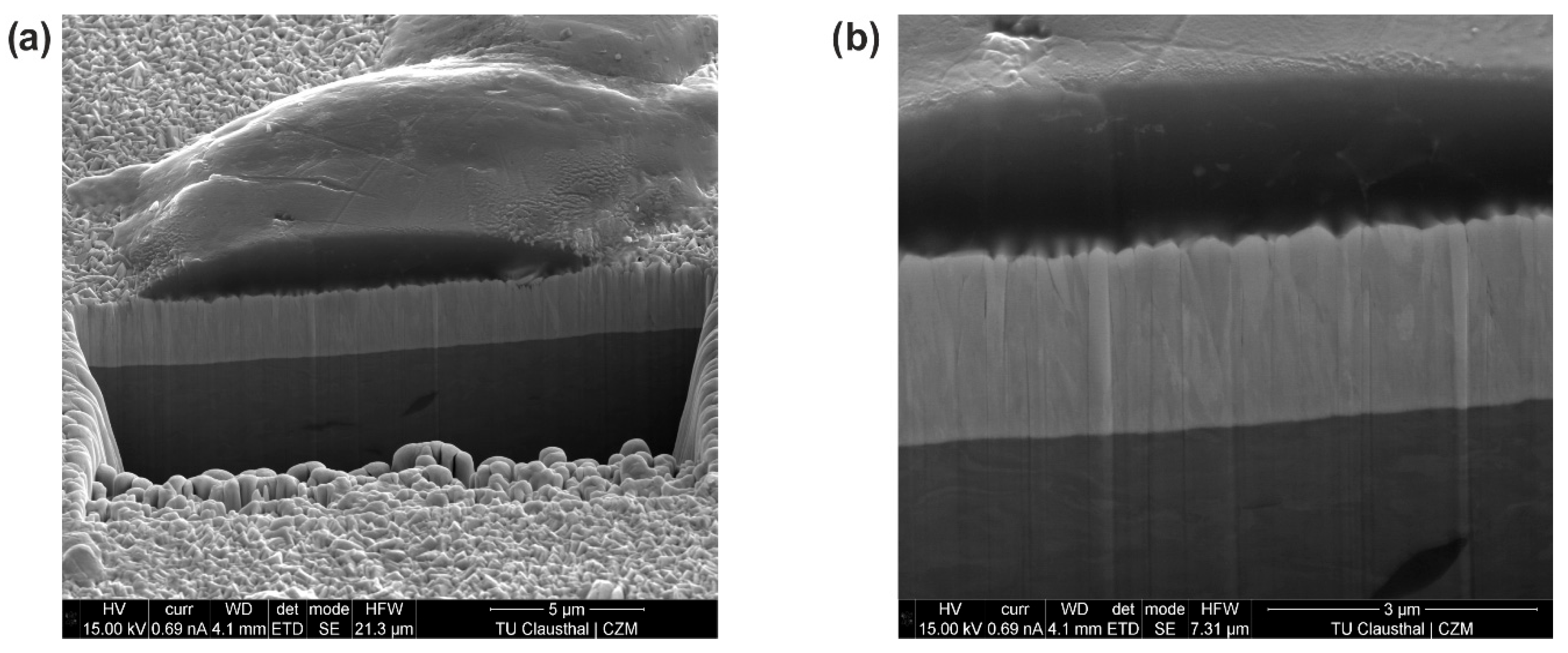
During the welding process, the respective diffusion barriers were in direct contact with aluminum at high temperatures. This led to a change in the electrode working face in the form of aluminum adhesions. These adhesions can occur primarily in the solid state or through the wetting of molten material. The extent to which adhesion occurred on the electrode working faces and diffusion through the barriers is shown in the following. The two diffusion barriers Ni (3.0 µm) and W (2.5 µm) were examined after the welding experiments in the area of the electrode working face and in the cross-section (Figure 8 and Figure 9).
Figure 8.
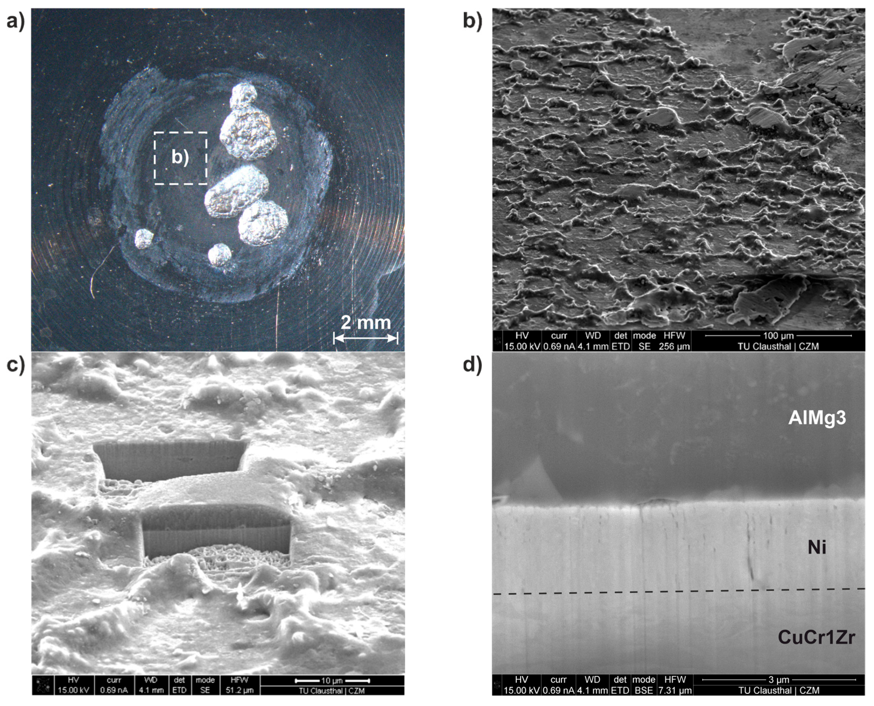
Ni diffusion barrier: degraded electrode working face (a); area of aluminum adhesion (b); sample cutting by focused ion beam (c); cross-section of Ni diffusion barrier (d).
Figure 9.
W diffusion barrier: area of aluminum adhesion (a) and cross-section of W diffusion barrier (b).
The Ni-coated electrode was examined by SEM in the degraded contact area after 108 welds. The focus, here, was on the surface area outside the pitting effects (Figure 8a). In this area, there are aluminum adhesions with a low-layer thickness and an irregular distribution. Due to the surface structure, it was assumed that the deposits were primarily in the solid state (Figure 8b). A focused ion beam was used to make an incision in the surface, allowing the structure of the diffusion barrier and the adhesion to be visualized in detail (Figure 8c). The aluminum adhesions occurred either through solid-state contact or through a partially molten component. It was, therefore, assumed that the locally occurring temperatures were in the range of the solidus line of the aluminum alloy. However, clear evidence of the temperatures occurring cannot be provided by the SEM images alone. It can be seen that despite the aluminum adhesions, the dendritic surface structure of the diffusion barrier was still intact (Figure 8d). The W coating as a diffusion barrier was examined using the same procedure (Figure 9).
After ten welds, the W coating showed aluminum adhesions, with a higher layer thickness compared to the Ni-coated electrodes. These adhesions have a highly irregular distribution on the electrode working face (see Figure 8 for a comparison). In this case, the adhesions originated from the liquid phase of the sheet material, which adhered to the dendritic structure in a droplet shape (Figure 9a). It can be assumed that the adhesions inhibited adequate contact between the electrode and the sheet material for further welding operations. This leads to a negative influence on the electrode–sheet contact, which prevents reproducibility of the current density and heat dissipation. Subsequent welds can, therefore, generate locally higher current densities and accelerate local damage to the diffusion barrier. The liquid-state adhesion led to complete wetting with the dendritic surface of the W coating (Figure 9b). After solidification of the aluminum adhesions and disengagement of the electrodes, the affected areas of the coating can be subject to tensile stress, which can promote local delamination of the coating. The occurrence of liquid-state adhesion could be due to the lower thermal conductivity of the W coating.
The diffusion barriers Ni and W achieved different performance levels in the resistance spot welding of aluminum alloys. Ni led to a significant increase in the achievable electrode life and a reduction in imperfections. W tended to cause strong adhesion of aluminum, resulting in early damage to the diffusion barrier. In order to be able to evaluate the diffusion tendency of aluminum through the individual barriers, EDX measurements were carried out on the sample incisions (Figure 10).
Figure 10.
EDX mapping (examination areas are marked in SEM-overviews in yellow boxes): diffusion barriers after electrode life examinations, Ni (a) and W (b).
The EDX mappings along the respective diffusion barriers also show the element distribution of Al and Cu. It can be seen that aluminum is only present on the surface of both diffusion barriers and is not found within the barrier. Therefore, it is assumed that aluminum neither diffuses transcrystalline nor across the grain boundaries to a greater extent. Small amounts of Cu are detected within the barrier layers. It cannot be completely avoided that Cu diffuses within the PVD coating into the forming barrier. However, it is more likely that due to the angle of beam incidence and the penetration depth of the EDX measurement, the Cu layer behind it was contained in the measurement signal in a low concentration.
3.5. Diffusion Experiments
No diffusion of aluminum through the barriers Ni and W occurred during the electrode life tests. Since the temperatures occurring in the electrode–sheet metal contact are not constant during the welding process, it is not possible to fully evaluate the suitability of Ni and W as functional barrier coatings. To allow a more accurate examination of the diffusion processes at a constant temperature, the CuCr1Zr samples coated with Ni and W were heated in a furnace under an inert atmosphere. For this purpose, the samples were coated with an additional layer of Al that was approximately 500 nm thick. The experiments were carried out in a furnace under an argon atmosphere. The temperature was set to 600 °C, as this corresponds to the expected maximum temperatures in contact between the electrode and the sheet metal during the welding process. After 60 min, the samples were removed and examined in cross-section using EDX (Figure 11).
Figure 11.
EDX mapping—diffusion barriers after diffusion experiments: Ni (a) and W (b).
Even at a constant temperature of 600 °C, the diffusion barriers showed no diffusion of Al after 60 min. The deposited Al layer remained on the respective barriers and did not diffuse deeper into the material beyond the grain boundaries. The results are similar to the EDX measurements of the coated electrodes after the electrode life tests (see Figure 10). Therefore, Ni and W can be considered as suitable barriers against the diffusion of Al.
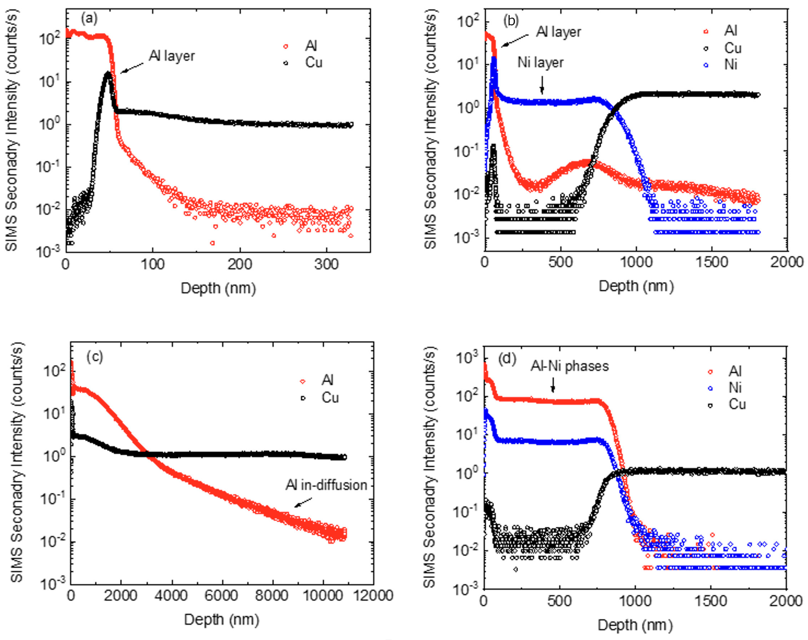
In addition to the EDX experiments, experiments with secondary ion mass spectrometry (SIMS) in the depth profile mode were carried out with a high spatial resolution in the nanometer range and a superior detection level of Al in the ppm range. As a model system, an AlMg3 tracer layer (70 nm) was deposited on a CuCr1Zr electrode without and with a Ni barrier layer of about 1 µm, using ion-beam sputtering. The corresponding SIMS profiles are shown in Figure 12a,b. The SIMS secondary intensity is a qualitative measure for the concentration of the respective element. The Al and Ni layers are clearly visible. The temporary increases in the Cu and Ni signals at the interface are artefacts due to the change of the ionization probability at the interface and, therefore, can be neglected. The samples were then annealed isothermally at 600 °C for 5130 s (~1.5 h). The time period was chosen so that there was sufficient duration for interdiffusion in the CuCr1Zr base material for the tracers used. It can be seen that for the samples without a barrier layer, the Al initially located at the surface diffuses deep into the sample during annealing up to 1 µm (Figure 12c). However, the sample with a Ni barrier layer shows unchanged stability at 600 °C and complete prevention of Al diffusion into the Cu (Figure 12d), which is in agreement with the EDX results. The strong increase in the Al signal within the region of the Ni layer, and the expansion of the layer thickness, can be explained here by the formation of Ni-Al intermetallic phases. Such phases generally show very low metal diffusion coefficients. Possible candidates are the NiAl or Ni3Al phases, with diffusion coefficients of only 10–20 respectively 10–22 m2/s at 600 °C [35,36]. This corresponds to maximum diffusion lengths of only 10 nm for the given annealing time, meaning that Al cannot cross the barrier. Cu(Al) and intermetallic CuAl phases show significantly faster diffusion [37]. The fact that the EDX measurements see no significant concentration of Al in the Ni layer might be due to the limited detection sensitivity of this method, of some single at.-%, which would indicate a Ni layer with a low Al concentration. Otherwise, the contradictory results are unexplained at the moment and need further clarification in the future. Note that diffusion in pure Ni is also relatively slow (10–19 m2/s at 600 °C) [38] and, as such, could explain the working of the barrier coating.
Figure 12.
SIMS depth profiles of AlMg3 on CuCr1Zr electrodes after deposition (a) without and (b) with a Ni barrier layer. The same samples annealed for 5130 s at 600 °C (c) without and (d) with barrier layer.
4. Conclusions
Resistance spot welding of aluminum alloys causes degradation of the electrode caps—Al-Cu alloy phases and intermetallic phases form, which can be analyzed in detail using nanoindentation and SEM analyses.
- In the area of intermetallic phase formation, the δ and Θ phases were detected.
- The hardness of the intermetallic phase boundary is 7.3–8.7 GPa, and the modulus of elasticity is up to 158.9 GPa.
- The hardness of the unaffected electrode material CuCr1Zr is 2.9 GPa, and the modulus of elasticity is 135.6 GPa.
- In order to differentiate between the mechanical properties of the two intermetallic phases, reduced measurement distances < 500 nm will be required for nanoindentation in the future.
Diffusion barriers composed of tungsten and nickel were investigated to limit electrode degradation. The barriers destroy the natural oxide layer of the AlMg3 material due to their dendritic structure, thereby reducing the electrical contact resistance between the electrode and the sheet material.
- The contact resistance between the reference electrode CuCr1Zr and an AlMg3 sheet material is 210 µOhm.
- An additional diffusion barrier reduces the contact resistance noticeably—83 µOhm (Ni) and 55 µOhm (W).
The properties of the diffusion barriers were also determined by nanoindentation. The coefficient of friction was evaluated by a scratch test method.
- The coefficient of friction of the reference electrode CuCr1Zr is 0.24.
- Additional diffusion barriers reduce the friction coefficient to 0.15 (W) and 0.16 (Ni).
- The hardness and elasticity moduli of the barriers are 18.5 GPa and 394.1 GPa (W); 6.7 GPa and 180.3 GPa (Ni).
The tungsten coating showed significant adhesion of aluminum during the first welds. Due to the adhesion, damage to the coating was accelerated, which meant that it was not possible to increase the electrode life. Nickel showed significantly delayed degradation. This increased the electrode lifetime by 86%. No diffusion of aluminum through the barriers was observed in either the welding or diffusion experiments by using EDX analysis. It was shown that the resolution of the EDX method is limited, and that only SIMS leads to differentiated results. The results of the SIMS analysis show that intermetallic phases form in the Ni-Al system. These have a significantly reduced diffusion rate for Al. This could explain the long electrode life of the Ni diffusion barriers.
Author Contributions
Conceptualization, S.B. and H.W.; methodology, S.B., J.J., H.W. and H.S.; validation, H.W., H.S. and V.W.; formal analysis, S.B., J.J. and R.G.; investigation, S.B. and J.J.; data curation, S.B. and J.J.; writing—original draft preparation, S.B., J.J. and H.S.; writing—review and editing, H.W. and H.S.; visualization, S.B., J.J., R.G. and H.S.; supervision, H.W. and H.S.; project administration, H.S. and V.W.; funding acquisition, H.W., H.S. and V.W. All authors have read and agreed to the published version of the manuscript.
Funding
This work was funded by the Deutsche Forschungsgemeinschaft (DFG, German Research Foundation), WE 2846/31-1 and SCHM 1569/40-1. The financial support is gratefully acknowledged.
Data Availability Statement
The raw data supporting the conclusions of this article will be made available by the authors on request.
Conflicts of Interest
The authors declare no conflicts of interest.
Abbreviations
The following abbreviations are used in this manuscript:
| DC | direct current |
| EDX | energy dispersive X-ray spectroscopy |
| L | liquid state |
| PVD | physical vapor deposition |
| S | solid state |
| SEM | scanning electron microscope |
| SIMS | secondary ion mass spectrometry |
| SPM | scanning probe microscopy |
| t | sheet thickness |
References
- Hirsch, J. Aluminium in Innovative Light-Weight Car Design. Mater. Trans. 2011, 52, 818–824. [Google Scholar] [CrossRef]
- Fukumoto, S.; Lum, I.; Biro, E.; Boomer, D.R.; Zhou, Y. Effects of Electrode Degradation on Electrode Life in Resistance Spot Welding of Aluminum Alloy 5182. Weld. J. 2003, 82, 307S–312S. [Google Scholar]
- Chang, B.H.; Du, D.; Chen, Q.; Zhou, Y. Studies on Effects of Pitting Morphology in Resistance Spot Welding of Aluminium Alloy. Sci. Technol. Weld. Join. 2007, 12, 67–72. [Google Scholar] [CrossRef]
- Lum, I.; Fukomoto, S.; Biro, E.; Boomer, D.R.; Zhou, Y. Electrode Pitting in Resistance Spot Welding of Aluminum Alloy 5182. Metall. Mater. Trans. A 2004, 35, 2217–2226. [Google Scholar] [CrossRef]
- Manladan, S.M.; Yusof, F.; Ramesh, S.; Fadzil, M.; Luo, Z.; Ao, S. A review on resistance spot welding of aluminum alloys. Int. J. Adv. Manuf. Technol. 2017, 90, 605–634. [Google Scholar] [CrossRef]
- Patrick, E.P.; Auhl, J.R.; Sun, T.S. Understanding the Process Mechanisms Is Key to Reliable Resistance Spot Welding Aluminum Auto Body Components. SAE Trans. 1984, 93, 435–448. [Google Scholar]
- Kunze, S. Beitrag zur Erhöhung der Prozesssicherheit beim Punktschweißen und Punktschweißkleben von Aluminiumkarosseriewerkstoffen; Berichte aus dem Laboratorium für Werkstoff- und Fügetechnik; Shaker: Aachen, Germany, 2014; Volume 100, ISBN 978-3-8440-2456-2. [Google Scholar]
- Schulz, E.; Mahjoubi, A.; Wagner, M.; Schubert, H.; Balasubramanian, B.; Brewer, L.N. Electrode Wear in Short-Pulse Resistance Spot Welding of Aluminum AA 6016-T4. Weld. World 2021, 65, 127–141. [Google Scholar] [CrossRef]
- Han, L.; Thornton, M.; Boomer, D.; Shergold, M. Effect of Aluminium Sheet Surface Conditions on Feasibility and Quality of Resistance Spot Welding. J. Mater. Process. Technol. 2010, 210, 1076–1082. [Google Scholar] [CrossRef]
- Liu, Q.; Li, Y.; Mao, X.; Zhao, P. Study on life of resistance spot welding copper electrode of 5182-H111 aluminum alloy for automobile. MW Met. Form. 2025, 7, 52–62. [Google Scholar]
- Gáspár, M.; Dobosy, Á.; Tisza, M.; Török, I.; Dong, Y.; Zheng, K. Improving the Properties of AA7075 Resistance Spot-Welded Joints by Chemical Oxide Removal and Post Weld Heat Treating. Weld. World 2020, 64, 2119–2128. [Google Scholar] [CrossRef]
- Rashid, M.; Fukumoto, S.; Medley, J.; Villafuerte, J.; Zhou, Y. Influence of Lubricants on Electrode Life in Resistance Spot Welding of Aluminum Alloys. Weld. J. 2007, 86, 62–70. [Google Scholar]
- Bamberg, P.; Seewald, R.; Schiebahn, A.; Reisgen, U.; Precoma, N.; Epperlein, M. Improvement of the Resistance Spot Welding of Al-Mg-Si Alloys by Using Cladding Technology: An Optical and Mechanical Characterization Study. J. Adv. Join. Process. 2022, 5, 100090. [Google Scholar] [CrossRef]
- Heilmann, S.; Baumgarten, M.; Koal, J.; Zschetzsche, J.; Füssel, U. Electrode Wear Investigation of Aluminium Spot Welding by Motion Overlay. Int. J. Adv. Manuf. Technol. 2022, 123, 749–760. [Google Scholar] [CrossRef]
- Heilmann, S.; Tulke, M.; Mathiszik, C.; Baumgarten, M.; Koal, J.; Brosius, A.; Füssel, U.; Schmale, H.C. Extending the Life of Aluminum Spot Welding Electrodes through Oxide Layer Disruption. Weld. World 2025. [Google Scholar] [CrossRef]
- Heilmann, S.; Zwahr, C.; Knape, A.; Zschetzsche, J.; Lasagni, A.F.; Füssel, U. Improvement of the Electrical Conductivity between Electrode and Sheet in Spot Welding Process by Direct Laser Interference Patterning. Adv. Eng. Mater. 2018, 20, 1700755. [Google Scholar] [CrossRef]
- Li, M.; Wang, Y.; Yang, S.; Tao, W.; Zhang, G. Improving Mechanical Properties and Electrode Life for Joining Aluminum Alloys with Innovatively Designated Newton Ring Electrode. J. Manuf. Process. 2021, 64, 948–959. [Google Scholar] [CrossRef]
- Brechelt, S.; Wiche, H.; Junge, J.; Gustus, R.; Schmidt, H.; Wesling, V. Increase of Electrode Life in Resistance Spot Welding of Aluminum Alloys by the Combination of Surface Patterning and Thin-Film Diffusion Barriers. Weld. World 2023, 67, 2703–2714. [Google Scholar] [CrossRef]
- Zhu, Y.; Wang, Y.; Bai, J.; Yang, S.; Zhu, Z.; Li, Q. Mechanism of Pitting-Adhesion Coupling in Aluminum Alloy Resistance Spot Welding Electrodes and Optimization of Asymmetric Electrode Configuration. J. Mater. Process. Technol. 2025, 342, 118942. [Google Scholar] [CrossRef]
- Park, H.; Kumar, D.; Park, K.; Nam, K.S.; Kim, Y.; Kim, Y.-M.; Lee, T. Electrode Life Evaluation for Varied Electrode Material Composition and Geometry in Resistance Spot Welding of Aluminum Alloys. Weld. World 2024, 68, 2701–2712. [Google Scholar] [CrossRef]
- Gradinger, R.; Sotirov, N.; Rettenbacher, G.; Pangerl, C.; Dörner, P.; Minichshofer, S.; Becirovic, A.; Melzer, C.; Uffelmann, D. High Strength Aluminium Sheet Metal Joining by Resistance Spot Welding. Mater. Sci. Forum 2013, 765, 761–765. [Google Scholar] [CrossRef]
- Chan, K.R.; Scotchmer, N.S. Quality and Electrode Life Improvements to Automotive Resistance Welding of Aluminum Sheet. In Proceedings of the Sheet Metal Welding Conference XIII., Livonia, MI, USA, 14–16 May 2008. [Google Scholar]
- Luo, P.; Dong, S.J.; Mei, Z.Q.; Xie, Z.X. Strengthening Mechanism of TiB2-TiC Complex Phases Coated Electrode. Adv. Mater. Res. 2012, 433–440, 251–255. [Google Scholar] [CrossRef]
- Luo, P.; Dong, S.; Yangli, A.; Sun, S.; Zheng, Z. Electrospark Deposition of ZrB2-TiB2 Composite Coating on Cu-Cr-Zr Alloy Electrodes. Int. J. Surf. Sci. Eng. 2016, 10, 41–54. [Google Scholar] [CrossRef]
- Luo, P.; Dong, S.; Yangli, A.; Sun, S.; Zheng, Z.; Wang, H. Electrospark Deposition of Al2O3–TiB2/Ni Composite-Phase Surface Coatings on Cu–Cr–Zr Alloy Electrodes. J. Asian Ceram. Soc. 2015, 3, 103–107. [Google Scholar] [CrossRef]
- Glagola, M.; Roest, C. Nickel Plated Electrodes for Spot Welding Aluminum. SAE Trans. 1976, 85, 780–794. [Google Scholar] [CrossRef]
- Hedenqvist, P.; Jacobson, S.; Hogmark, S. Tribological PVD Coatings—Characterisation of Mechanical Properties. Surf. Coat. Technol. 1997, 97, 212–217. [Google Scholar] [CrossRef]
- Tayebi, N.; Polycarpou, A.A.; Conry, T.F. Effects of Substrate on Determination of Hardness of Thin Films by Nanoscratch and Nanoindentation Techniques. J. Mater. Res. 2004, 19, 1791–1802. [Google Scholar] [CrossRef]
- Wang, X.; Xu, P.; Han, R.; Ren, J.; Li, L.; Han, N.; Xing, F.; Zhu, J. A Review on the Mechanical Properties for Thin Film and Block Structure Characterised by Using Nanoscratch Test. Nanotechnol. Rev. 2019, 8, 628–644. [Google Scholar] [CrossRef]
- Saha, R.; Nix, W.D. Effects of the Substrate on the Determination of Thin Film Mechanical Properties by Nanoindentation. Acta Mater. 2002, 50, 23–38. [Google Scholar] [CrossRef]
- Mao, A.; Zhang, J.; Yao, S.; Wang, A.; Wang, W.; Li, Y.; Qiao, C.; Xie, J.; Jia, Y. The Diffusion Behaviors at the Cu-Al Solid-Liquid Interface: A Molecular Dynamics Study. Results Phys. 2020, 16, 102998. [Google Scholar] [CrossRef]
- Yang, C.-W. Tensile Mechanical Properties and Failure Behaviors of Friction Stir Processing (FSP) Modified Mg-Al-Zn and Dual-Phase Mg-Li-Al-Zn Alloys. In Materials Science—Advanced Topics; IntechOpen: London, UK, 2013; ISBN 978-953-51-1140-5. [Google Scholar] [CrossRef]
- Zobac, O.; Kroupa, A.; Zemanova, A.; Richter, K.W. Experimental Description of the Al-Cu Binary Phase Diagram. Metall. Mater. Trans. A 2019, 50, 3805–3815. [Google Scholar] [CrossRef]
- Bauer, C.L.; Lessmann, G.G. Metal-Joining Methods. Annu. Rev. Mater. Sci. 1976, 6, 361–387. [Google Scholar] [CrossRef]
- Divinski, S.V.; Herzig, C. Ni Tracer Self-Diffusion, Interdiffusion and Diffusion Mechanisms in NiAl. Defect Diffus. Forum 2002, 203, 177–192. [Google Scholar] [CrossRef]
- Frank, S.T.; Södervall, U.; Herzig, C. Self-Diffusion of Ni in Single and Polycrystals of Ni3Al. A Study of SIMS and Radiotracer Analysis. Phys. Status Solidi B 1995, 191, 45–55. [Google Scholar] [CrossRef]
- Romig, A.D., Jr. Interdiffusion in β phase Cu–Al alloys. J. Appl. Phys. 1983, 54, 3172–3175. [Google Scholar] [CrossRef]
- Neumann, G. Self-Diffusion and Impurity Diffusion in Pure Metals: Handbook of Experimental Data, 1st ed.; Pergamon Materials Series; Pergamon: Amsterdam, The Netherlands, 2009. [Google Scholar]
Disclaimer/Publisher’s Note: The statements, opinions and data contained in all publications are solely those of the individual author(s) and contributor(s) and not of MDPI and/or the editor(s). MDPI and/or the editor(s) disclaim responsibility for any injury to people or property resulting from any ideas, methods, instructions or products referred to in the content. |
© 2025 by the authors. Licensee MDPI, Basel, Switzerland. This article is an open access article distributed under the terms and conditions of the Creative Commons Attribution (CC BY) license (https://creativecommons.org/licenses/by/4.0/).