Abstract
The rapid advancement of high-performance electronics has intensified the demand for wide-bandgap semiconductor materials capable of operating under high-power and high-temperature conditions. Among these, silicon carbide (SiC) has emerged as a leading candidate due to its superior thermal conductivity, chemical stability, and mechanical strength. However, the high cost and complexity of SiC wafer fabrication, particularly in slicing and exfoliation, remain significant barriers to its widespread adoption. Conventional methods such as wire sawing suffer from considerable kerf loss, surface damage, and residual stress, reducing material yield and compromising wafer quality. Additionally, techniques like smart-cut ion implantation, though capable of enabling thin-layer transfer, are limited by long thermal annealing durations and implantation-induced defects. To overcome these limitations, ultrafast laser-based processing methods, including laser slicing and stealth dicing (SD), have gained prominence as non-contact, high-precision alternatives for SiC wafer exfoliation. This review presents the current state of the art and recent advances in laser-based precision SiC wafer exfoliation processes. Laser slicing involves focusing femtosecond or picosecond pulses at a controlled depth parallel to the beam path, creating internal damage layers that facilitate kerf-free wafer separation. In contrast, stealth dicing employs laser-induced damage tracks perpendicular to the laser propagation direction for chip separation. These techniques significantly reduce material waste and enable precise control over wafer thickness. The review also reports that recent studies have further elucidated the mechanisms of laser–SiC interaction, revealing that femtosecond pulses offer high machining accuracy due to localized energy deposition, while picosecond lasers provide greater processing efficiency through multipoint refocusing but at the cost of increased amorphous defect formation. The review identifies multiphoton ionization, internal phase explosion, and thermal diffusion key phenomena that play critical roles in microcrack formation and structural modification during precision SiC wafer laser processing. Typical ultrafast-laser operating ranges include pulse durations from 120–450 fs (and up to 10 ps), pulse energies spanning 5–50 µJ, focal depths of 100–350 µm below the surface, scan speeds ranging from 0.05–10 mm/s, and track pitches commonly between 5–20 µm. In addition, the review provides quantitative anchors including representative wafer thicknesses (250–350 µm), typical laser-induced crack or modified-layer depths (10–40 µm and extending up to 400–488 µm for deep subsurface focusing), and slicing efficiencies derived from multi-layer scanning. The review concludes that these advancements, combined with ongoing progress in ultrafast laser technology, represent research opportunities and challenges in transformative shifts in SiC wafer fabrication, offering pathways to high-throughput, low-damage, and cost-effective production. This review highlights the comparative advantages of laser-based methods, identifies the research gaps, and outlines the challenges and opportunities for future research in laser processing for semiconductor applications.
1. Introduction
Silicon carbide (SiC) has emerged as a leading material for next-generation integrated circuits and power electronic applications due to its outstanding physical, electronic, and optical properties [1,2]. Among its various polytypes, 4H- and 6H-SiC are particularly attractive owing to their wide bandgap, high thermal conductivity, high breakdown electric field, and superior carrier mobility [3]. These properties make SiC a prime candidate for high-power, high-frequency, and high-temperature applications, setting it apart as a third-generation semiconductor material [4]. One of the most significant developments in this field is the advancement of semi-insulating (SI) SiC substrates, especially 4H-SiC, which have been demonstrated to be highly suitable for the fabrication of high-electron-mobility transistors (HEMTs) used in microwave and radio frequency (RF) devices [5]. Si-SiC substrates provide excellent electrical isolation and thermal management, which are essential for the performance and reliability of high-frequency electronics operating in extreme environments. With the ongoing deployment of 5G networks, the demand for SiC-based components is rapidly increasing due to their ability to operate efficiently at high power densities and elevated temperatures. In particular, Si-SiC is expected to play a pivotal role in enabling the next generation of high-frequency communication systems, where low loss, high isolation, and thermal robustness are critical. Furthermore, SiC devices are being increasingly adopted in a range of high-power and high-voltage applications. These include hybrid electric vehicles (HEVs), plug-in electric vehicles (PEVs), and battery electric vehicles (BEVs), where SiC-based power electronics offer significant improvements in efficiency and thermal performance [1,3,4]. Beyond transportation, SiC is also being utilized in high-power RF applications, high-temperature sensor circuits suitable for harsh environments such as jet engine blocks, ultraviolet (UV) photodetectors [6], nuclear and ionizing radiation detectors [7], and corrosion-resistant microelectromechanical systems (MEMS) and sensors [8,9].
As research continues to optimize material quality and device architectures, the role of SiC—particularly SI 4H- and 6H-SiC—is expected to expand across a broad range of advanced electronic systems. This paper reviews recent developments and highlights the growing importance of SiC technology in supporting emerging applications that demand high performance in extreme operational conditions. Despite its advantages, the mass production of SiC remains considerably more challenging than that of traditional silicon, which continues to limit SiC’s widespread adoption in the mainstream chip industry. Single crystal SiC wafers are significantly more expensive (often 5–10× or more) than Si wafers due to SiC’s complex, high-temperature growth process, smaller available sizes, lower yields, higher defect rates, and the immense difficulty in handling the hard and brittle material.
Traditional exfoliation methods such as wire sawing offer scalability but suffer from low material yield due to substantial kerf loss during the cutting process (Figure 1a). In particular, the kerf loss caused by the wire and slurry in these processes can reach approximately 250 μm [10]. Wire sawing technologies—primarily multi-wire slurry sawing and diamond wire sawing—are the most widely used methods for slicing SiC wafers, offering relatively high throughput and production efficiency [11]. However, these methods face limitations in achieving ultra-thin wafers, necessitating additional post-processing steps such as grinding and polishing to reach the desired thickness. Moreover, many SiC wafer products exhibit poor quality due to damage defects and residual stress introduced during contact-based machining processes. Specifically, electroplated diamond wire sawing often leads to subsurface microcrack damage and significant stress, which compromises wafer integrity [12,13]. Additionally, the sawing of SiC single crystals containing void defects can further exacerbate stress concentration and surface irregularities [13]. Similar issues have also been observed in silicon-based materials, where residual stresses induced by wire sawing and casting negatively affect wafer flatness and structural reliability [14]. These challenges underline the need for non-contact or minimally invasive slicing technologies to improve the quality and reliability of SiC wafers. As a result, considerable research efforts have been dedicated to developing advanced exfoliation techniques that minimize material loss while improving yield, with the goal of enabling more cost-effective and efficient SiC wafer production.
Novel laser-based techniques for SiC wafer processing such as SiC exfoliation, laser slicing, and stealth dicing have emerged as promising alternatives to overcome these limitations, offering non-contact, dry processes with reduced damage and higher precision. A comprehensive review is needed to synthesize the latest advancements in these technologies to facilitate their broader industrial application and address the increasing demand for high-quality SiC devices.
The primary rationale for this review is to provide a structured and critical analysis of the various laser-assisted processing methods for SiC wafers. While existing research highlights the potential of these techniques, the information is fragmented across numerous individual studies focusing on specific parameters or outcomes.
The ion-implantation method, (see Figure 1b) particularly smart-cut technology, has also been explored to produce thinner SiC wafers. While this technique enables the transfer of thin crystalline layers, it often introduces implantation-induced defects into the material, adversely affecting wafer quality and device performance [15,16,17]. These damage mechanisms—such as extended defects, hydrogen-induced blistering, and surface roughness—remain significant challenges that limit the viability of ion implantation for high-yield, high-quality SiC exfoliation. Additionally, pulsed laser-assisted exfoliation has been investigated as a method to enhance the detachment of hydrogen ion-implanted SiC thin layers, offering a potential pathway to reduce damage and improve wafer quality compared to conventional ion implantation techniques [18,19].

Figure 1.
(a) Wire sawing (diamond wire diameters typically range from 60 to 120 μm) [13], (b) ion implantation (typical ion implantation depths range from 50 nm to 2 μm) [18,19,20,21], and (c) slicing using pulsed lasers (focused spot size range from 1 to 20 μm) (laser focus beneath the surface ranges from 50 to 300 μm deep into substrate) [22,23].
With rapid advancements in ultrafast laser technology, lasers—especially ultrafast lasers—have become vital tools for efficient exfoliation of SiC layers from bulk material (see Figure 1c). One such method is laser slicing, where laser pulses are focused at a specific depth within the bulk SiC, corresponding to the desired layer thickness (see Figure 2a). Multiple damage tracks are inscribed with appropriate dot spacing side-by-side perpendicular to the exfoliation plane. Microcracks formed around these damage tracks intersect and propagate, creating larger cracks that allow the SiC layer to be mechanically separated after laser processing. Another related technique is stealth dicing, which shares a similar principle but differs in laser orientation (see Figure 2b).
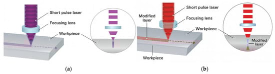
Figure 2.
(a) Laser slicing (ablation) (focused spot size: 1–20 μm typically and 5–20 μm for faster processing), (b) stealth dicing (SD) (focus spot size: 1–5 μm for stealth dicing). (arrow represents scanning direction).
Here, laser pulses with appropriate dot spacing propagate parallel to the exfoliation plane, forming a modified layer (decomposed crystalline) that facilitate wafer dicing into chips. Thus, the key difference between laser slicing and stealth dicing lies in the orientation of the modified layers relative to the laser propagation: laser slicing creates modified layers parallel to the laser direction for wafer slicing, while stealth dicing forms layers perpendicular to the laser propagation to dice wafers and it is possible to leave no scratches on the SiC surface. Laser slicing, which uses internal laser-modified layers combined with external mechanical force to separate wafers, offers a promising solution to challenges such as kerf loss and material damage. Laser slicing uses water-soluble film and ablation that can achieve high quality without chipping or cracking when compared to mechanical methods such as wire sawing technologies. Stealth dicing is a dry process that can make extremely thin kerf width with little waste.
Hirata et al. [24] demonstrated that laser slicing is approximately 92% more efficient than traditional wire sawing and reduces material loss by half [24]. This technique allows precise control over wafer thickness by adjusting the depth of the modified layer and enables kerf-loss-free slicing, significantly improving material utilization. It is important to emphasize that despite both laser slicing and stealth dicing utilizing laser-induced internal modifications for material separation, they are distinct processes with different applications: laser slicing targets wafer separation using layers parallel to laser propagation, while stealth dicing focuses on chip separation using layers perpendicular to the laser path [25].
Development of ultrafast lasers was especially important for laser slicing and stealth dicing processes since the minimization of thermal effects with ultrashort laser pulses also minimizes thermal defects typically occur after the laser processing of SiC. However, both of those processes are open to further improvement to minimize the surface roughness obtained after the layer separation as future research targets.
Meanwhile, silicon carbide-on-insulator (SiCOI) structures are increasingly recognized for their energy-efficient and radiation-tolerant characteristics. These structures are typically produced using smart-cut technology, which involves hydrogen ion implantation, wafer bonding, and high-temperature annealing. A critical factor in achieving successful layer transfer is the formation of micro-cracks, which are induced by platelet complexes of vacancies and hydrogen atoms. When the implanted depth is less than 1 µm, surface blistering and exfoliation can occur. The efficiency of exfoliation is influenced by several parameters, including the order of hydrogen and helium implantation. For materials such as gallium arsenide (GaAs) and silicon (Si), the co-implantation of hydrogen and helium has been demonstrated to reduce the total ion fluence required for exfoliation. This observation suggests a promising pathway to enhance the efficiency of the smart-cut process for SiC through novel co-implantation strategies [26].
A historical development timeline for SiC exfoliation, laser slicing, and stealth dicing is presented in Table 1 The table summarizes key milestones and technological breakthroughs that have enabled increasingly precise and efficient SiC wafer processing methods.

Table 1.
A historical development timeline for SiC exfoliation, laser slicing, and stealth dicing.
The literature review was conducted following a structured and systematic methodology. Relevant journal articles were identified using major scholarly databases such as Web of Science, Scopus, and Google Scholar, focusing on peer-reviewed publications related to advanced manufacturing processes. Keyword combinations included laser-based precision SiC wafer exfoliation processes, laser slicing, exfoliation, SiC polytypes (4H- and 6H-SiC single-crystal SiC), stealth dicing, ultrafast laser processing and slicing, ion implantation–assisted exfoliation, and conventional approaches such as wire sawing. Articles were screened based on relevance, technical depth, and recency, with priority given to studies that presented clear process mechanisms, modeling or experimental validation, and comparative insights across different SiC slicing and exfoliation technologies. Duplicates and non-peer-reviewed sources were excluded. A minimum of five high-quality journal articles were selected for each project to ensure comprehensive coverage of the state of the art and key technical challenges.
2. Current State of the Art: Literature Review
Typical processing routes for exfoliating layers from single crystal silicon carbide (SiC), specifically 4H-SiC or 6H-SiC, involve several established techniques. One common approach is ion implantation followed by thermal exfoliation (see Figure 3a).
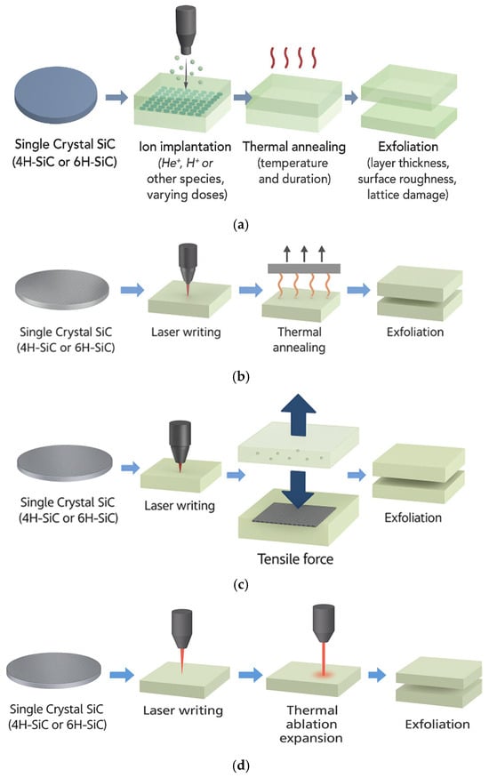
Figure 3.
Processing routes for (a) ion implantation and thermal exfoliation, (b) laser writing and thermal exfoliation, (c) laser writing and tensile exfoliation, and (d) laser writing and laser-assisted splitting. (wafer thicknesses (250–350 µm)).
In this method, the SiC substrate is first subjected to ion implantation using species such as He+, H+, or other ions, with carefully controlled doses. This is followed by a thermal annealing step, where the substrate is heated at specific temperatures for a defined duration. The combination of implantation-induced damage and thermal activation enables the exfoliation of the surface layer, characterized by specific layer thickness, surface roughness, and the extent of lattice damage. A second processing route involves laser writing followed by thermal exfoliation (see Figure 3b). Here, the single crystal SiC wafer is processed using laser slicing or stealth dicing techniques. Laser parameters such as pulse energy, dot spacing, repetition rate, and fluence are optimized to create subsurface modifications. These modified regions are then activated through thermal annealing, which leads to exfoliation of the upper layer. This method allows for control over exfoliated layer thickness, kerf width, surface roughness, and crystalline quality. A third technique eliminates the need for thermal annealing by combining laser writing with mechanical exfoliation (see Figure 3c). In this route, laser slicing or stealth dicing is again used to introduce internal modifications. Instead of heat treatment, a tensile force—often induced by mechanical or acoustic excitation—is applied to initiate and propagate the separation. This process also enables the release of thin layers, with control over thickness, kerf width, surface finish, and damage to the underlying lattice.
2.1. Ion Implantation and Thermal Annealing Exfoliation
You et al. [27] demonstrated that co-implantation of He and H2 ions into SiC at 1100 °C resulted in reduced exfoliation efficiency compared to single H implantation. Microstructural analysis revealed a high density of bubbles rather than the micro-cracks typically observed with H implantation alone, which explains the diminished surface exfoliation in the He and H co-implanted SiC. Single-crystal 6H-SiC samples were uniformly pre-implanted with He ions at two different fluence levels (low and high) and subsequently co-implanted with H ions at room temperature over a 16 × 17 mm2 area under vacuum conditions. Post-implantation thermal annealing was performed at 1100 °C for 15 min in vacuum (10−3 Pa). Lattice damage resulting from H2+ and He+ implantation was characterized using Raman spectroscopy, which detects variations in Raman scattering intensity, frequency shifts, and changes in phonon modes, as shown in Figure 4.
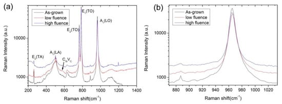
Figure 4.
(a) Raman spectra of as-grown SiC and SiC samples implanted with He ions at high and low fluences. (b) Magnified view of the A1(LO) phonon peaks, highlighting spectral differences due to ion implantation. Adapted from You et al. [27].
Raman spectroscopy results indicate that implantation-induced defects were not completely eliminated by the annealing process, primarily due to the formation of gas bubbles during annealing. Additionally, an increase in He fluence was found to reduce the crystallinity of the SiC. Microstructural changes (see Figure 5), including lattice defects and bubble formation, were further examined using cross-sectional transmission electron microscopy (XTEM) and high-resolution transmission electron microscopy (HRTEM).
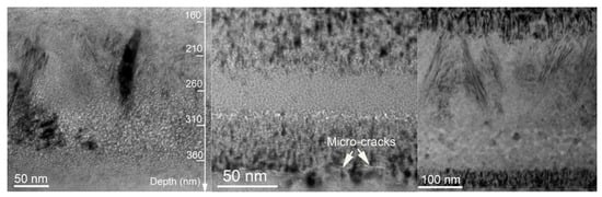
Figure 5.
Cross-sectional transmission electron microscopy (XTEM) images of the damaged layer showing (from (left) to (right)): bubble formation, micro-cracks, and dislocations. Adapted from You et al. [27].
You et al. [27] state that, unlike in silicon, helium co-implantation does not enhance exfoliation efficiency in SiC. This behavior is attributed to the significantly higher migration energy of He atoms compared to other host materials, which promotes rapid accumulation of H2 gas and bubble formation. Moreover, due to this high migration energy, the implantation-induced defects in SiC are less responsive to thermal annealing than those in Si, as evidenced by the persistent spectral features observed in the Raman spectra. Microstructural observations also indicate that increasing He fluence leads to a higher bubble density within the implanted region.
2.2. Laser Slicing and Tensile Force Exfoliation
In another study, Kim et al. [10] investigated a laser slicing method for efficient exfoliation of SiC, specifically employing a double-pulse configuration. A femtosecond (fs) laser with a 1 kHz repetition rate was used, and a delay line was integrated into the optical path to enable double-pulse generation. This setup produced fs laser pulse trains consisting of two pulses, where the time delay between pulses could be modulated on the order of several picoseconds, while maintaining a constant pulse train repetition rate of 1 kHz (1 ms) (see Table 2).
Table 2.
Process parameters [10].
During process optimization, the researchers concluded that in a single-pulse configuration, picosecond (ps) laser pulses were more effective than fs pulses for generating modified layers suitable for laser slicing of SiC, as fs pulses did not produce significant modification. In contrast, the double-pulse fs configuration successfully generated a well-defined modified layer.
Structural analysis of the modified regions revealed disrupted crystallinity and the formation of amorphous carbon, as evidenced by the presence of G and D bands in Raman spectra. Furthermore, tensile testing showed that samples processed with the double-pulse fs configuration required significantly lower tensile stress for layer separation and exhibited improved surface roughness compared to those processed with single-pulse ps lasers. These findings suggest that the double-pulse fs configuration enhances the efficiency of laser slicing in SiC. as shown in Figure 6.
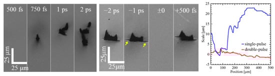
Figure 6.
From (left) to (right): (1) Morphologies of the modified layers produced using different laser pulse durations; (2) morphologies of the modified layers generated by femtosecond double-pulse trains with varying delay times (arrows indicate separation locations); and (3) comparison of surface roughness after separation for single-pulse and double-pulse configurations. Adapted from Kim et al. [10].
Zhang et al. [28] emphasized that, among the two primary types of SiC—N-doped and semi-insulating—the latter is gaining increasing attention due to its relevance in 5G applications. Despite this, relatively few studies have investigated the laser slicing of semi-insulating SiC. In their work, the authors employed a femtosecond (fs) laser with a pulse duration tunable into the picosecond (ps) range to study the laser slicing process over a broad range of parameters, including pulse duration, pulse energy, scan speed, track separation, and layer depth (see Table 3).
Table 3.
Process parameters [28].
Consistent with the findings of Kim et al. [10], they observed that ps-duration laser pulses were more effective than fs pulses in forming modified layers. The resulting modified regions typically consisted of SiC with degraded crystallinity and the presence of amorphous carbon, as indicated by the emergence of G and D bands in Raman spectra (see Figure 7). Interestingly, the researchers found that at sufficiently high pulse energies or low scan speeds, multiple modified layers could be formed along the laser propagation direction using ps pulses. However, they concluded that the formation of multiple modified layers is undesirable, as only samples with a single modified layer were successfully separated during tensile testing.
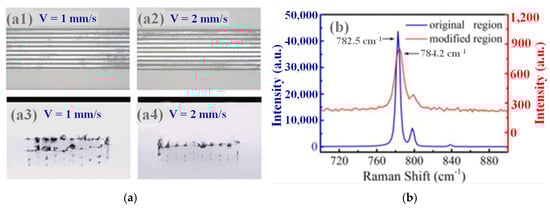
Figure 7.
(a) Confocal microscopy images showing (from (top) to (bottom)) the top view and cross-sectional view of (from (left) to (right)) single-layer and multiple-layer modified structures in SiC. (b) Raman spectra comparing bulk SiC and laser-modified regions. Adapted from Zhang et al. [28].
Chen et al. [29] conducted a comprehensive investigation into the effects of nitrogen doping concentration on the laser slicing of n-type 4H-SiC wafers to enhance slicing quality and broaden the process window. The study combined experimental analysis with a two-temperature model to assess how varying doping levels influence laser-material interactions, including absorption, crack formation, peeling strength, and surface roughness. Using a custom-built picosecond laser (15 ps, 1064 nm), laser-induced internal modifications were performed on SiC samples with five different doping levels, followed by mechanical exfoliation using tensile force and detailed surface characterization (see Table 4). Key findings of the study indicated that higher nitrogen doping increased the material’s free carrier absorption and electrical conductivity, leading to stronger laser absorption but reduced crack propagation length and modified line width [29]. Furthermore, Chen et al. [29] reported that the peeling strength required to separate the wafers increased with doping concentration, though this could be mitigated by optimizing laser power. Through both experimental validation and thermophysical modeling, the authors demonstrated that doping concentration critically affects laser energy deposition and thermal stress distribution, and they successfully achieved high-quality slicing of a 200 mm SiC wafer (Figure 8). This work provides valuable insight into optimizing laser parameters for slicing doped SiC wafers and extends the applicability of ultrafast laser slicing techniques to larger and more conductive substrates.
Table 4.
Process parameters [29].
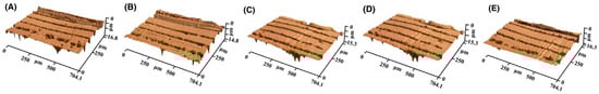
Figure 8.
Confocal microscopy images of separated surfaces (A–E) after optimizing [29].
2.3. Laser Stealth Dicing and Tensile Force Exfoliation
Yang et al. [22] investigated high-precision stealth dicing of SiC using a picosecond (ps) laser with a pulse width ranging from 1 ps to 10 ps to form modified dicing layers for chip fabrication. To achieve highly accurate dicing, the authors emphasized three key strategies: (i) The laser power was gradually reduced from 100% to 62% during the inscription of the modified dicing layer, starting from the bottom surface and progressing toward the top surface. A total of 20 parallel tracks were created along the thickness direction, with a vertical spacing of 24 µm (see Table 5). Each subsequent track was inscribed using a lower laser power to compensate for the transmission losses encountered as the laser propagated deeper into the material (see Figure 9a). (ii) The results revealed a linear relationship between the laser pulse width and the post-separation surface roughness, indicating that precise control of pulse duration directly impacts the quality of the dicing surface. (iii) Owing to the anisotropic nature of SiC, chips separated along the {10-10} crystallographic direction exhibited superior surface roughness compared to those diced along the {11-20} direction (see Figure 9b).
Table 5.
Process parameters [22].
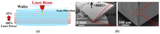
Figure 9.
(a) schematic illustration of the stealth dicing process, (b) SEM images of separated SiC chips, highlighting differences in surface roughness along different crystallographic directions (as indicated with the arrow). Adapted from Yang et al. [22].
Wang et al. [30] investigated the structural characteristics and defect formation mechanisms associated with stealth dicing (SD) of 4H-SiC wafers using ultrafast lasers—specifically femtosecond (270 fs) and picosecond (10 ps) pulses (see Table 6). Ultrafast pulsed lasers are considered promising tools for semiconductor wafer processing due to their high precision and minimal thermal damage. The study aimed to understand the underlying laser–material interactions by analyzing nonlinear refractive index behavior, laser beam propagation, energy absorption, electron concentration dynamics, and energy deposition in 4H-SiC.
Table 6.
Process parameters [30].
Femtosecond laser processing enabled higher machining precision due to the highly localized energy deposition. However, at lower energy densities, it resulted in unstable and discontinuous modified layers. The dominant defect mechanisms under fs irradiation were identified as multiphoton ionization and internal phase explosion, which led to the formation of nanovoids and micro-cracks. These microstructural features could accumulate with repeated scanning passes, potentially evolving into ablation-induced defects. In comparison, picosecond laser processing produced a larger modified zone, attributed to beam refocusing along the propagation path. This effect improved processing efficiency but also introduced more extensive amorphous ablation defects and structural damage. Such defects may compromise the mechanical integrity of the wafer and degrade device performance.
2.4. Laser Slicing and Photoelectrochemical Exfoliation
In their study, Geng et al. [31] demonstrated a quite unique way to exfoliate SiC. In their study, they employed laser slicing where a modified layer perpendicular to the laser propagation has been formed with a fs laser but instead of a mechanical or thermal stress to perform separation, they instead showed that there is a band gap difference between the bulk SiC and the modified layer due to the phase transitions occur during laser irradiation and researchers took the advantage of this feature by applying band gap selective photoelectrochemical (PEC) etching by utilizing a special chemical solution in assistance with applied voltage and UV light irradiation which in total takes 180 min (see Table 7). As a result, they acquired successful layer separation and post process Raman spectra shows that separated surfaces show the exact material properties with bulk SiC, meaning that modified layer successfully etched (material loss, a downside). Moreover, they obtained a better surface roughness with the novel PEC etching method when compared with the mechanical separation following the same laser slicing method (former has 1 µm roughness whereas latter has 5 µm).
Table 7.
Process parameters [31].
Geng et al. [31] demonstrated a novel approach for exfoliating SiC using laser slicing combined with bandgap-selective photoelectrochemical (PEC) etching (see Figure 10). In their study, a modified layer was formed perpendicular to the laser propagation direction using a femtosecond (fs) laser. Unlike conventional methods that rely on mechanical or thermal stress for layer separation, the authors exploited the bandgap difference between the bulk SiC and the laser-modified layer, which arises from phase transitions induced during laser irradiation.
Figure 10.
Schematic illustration comparing mechanical exfoliation (red arrows indicate force directions) and photoelectrochemical (PEC) exfoliation methods used for layer separation in SiC. (laser beam is in the [0001] crystalline direction) Adapted from Geng et al. [31].
To achieve selective removal of the modified layer, the researchers employed PEC etching using a specialized chemical solution in conjunction with applied voltage and UV light irradiation. The entire etching process was completed in approximately 180 min. Successful layer separation was achieved, and post-process Raman spectroscopy confirmed that the separated surfaces retained the intrinsic material properties of bulk SiC, indicating that the modified layer had been effectively removed, albeit with material loss as a trade-off.
Furthermore, surface roughness measurements revealed that the PEC etching method yielded significantly smoother surfaces (~1 µm roughness) compared to those obtained via mechanical separation following the same laser slicing process (~5 µm roughness). These findings suggest that PEC etching offers a promising alternative to conventional separation techniques, particularly for applications requiring minimal surface damage.
2.5. Laser Slicing and Laser-Assisted Splitting
Jiang et al. [32] introduced a novel continuous-wave (CW) laser-assisted splitting method for 4H-SiC wafers that utilizes a modified layer fabricated by picosecond laser pulses. Aiming to overcome the inefficiencies and material losses of traditional wire-sawing, their approach significantly enhances processing efficiency while minimizing mechanical stress. The methodology involves first forming an internal modified layer within the SiC substrate using a picosecond laser (1064 nm, 12.6 ps), which decomposes SiC into amorphous Si and C, greatly increasing the absorption of a subsequent CW laser at the same wavelength (see Table 8). The CW laser irradiation induces localized heating and thermal stress concentrated in the modified layer, which promotes crack initiation and propagation, leading to controlled wafer splitting without mechanical loading. Jiang et al. [32] combined experimental analysis with a two-dimensional thermal–mechanical finite element simulation to model the stress and temperature distributions. Results showed that laser-induced thermal stress (up to 400 MPa) exceeded the tensile strength of the modified SiC layer (10–40 MPa), enabling clean separation at optimized conditions (105 W power, 0.04 mm scan spacing). SEM, Raman, and XRD analyses confirmed that the split wafers retained their single-crystalline SiC structure, with a thin residual layer (50–250 nm) of polycrystalline carbon and recrystallized Si, which could be removed by post-processing. The process produced smoother surfaces compared to mechanical splitting, with improved roughness profiles and reduced material damage. This work demonstrates the potential of hybrid picosecond–CW laser processing as an efficient, non-contact method for precision slicing of SiC wafers.
Table 8.
Process parameters [32].
2.6. Other Laser Slicing Methods
Li et al. [33] developed a hybrid laser processing method that integrates nanosecond laser slicing with femtosecond laser polishing to improve material utilization and surface quality in single crystal 4H-SiC wafer preparation. The study aimed to overcome the high material loss and mechanical damage associated with conventional wire-sawing and grinding by implementing a kerf-free laser slicing technique followed by precise laser polishing. Using a nanosecond laser (532 nm, 200 ns pulse width, 60 kHz) for slicing, an internal modified layer was created via capsule-shaped exploding holes and microcrack propagation, allowing wafer separation with a peeling force of approximately 3.6 MPa (see Table 9). The sliced surfaces exhibited fluvial morphologies with an average roughness over Sa 0.89 μm and clear crystalline–amorphous transitions, as confirmed by SEM, Raman, and HRTEM analyses. Subsequent femtosecond laser polishing (517 nm, 650 fs, 50 kHz) significantly reduced the surface roughness to Sa 0.22 μm and transformed the microstructure through re-melting, Si–C bond dissociation, and formation of 3C-SiC and SiO2 phases. Notably, laser-induced periodic surface structures (LIPSS) and amorphous layers were observed post-polishing, evidencing surface reconstruction driven by high thermal gradients and ultrafast cooling. The hybrid process achieved up to 75% reduction in material loss compared to conventional methods, while preserving single crystallinity and minimizing subsurface damage. This study demonstrates a promising route for high-efficiency, damage-minimized fabrication of SiC substrates for semiconductor applications.
Table 9.
Process parameters [33].
Liu and Hong et al. [34] proposed an innovative all-laser processing strategy for slicing single-crystal 4H-SiC wafers, aimed at achieving ultra-low kerf-loss and high surface quality without the drawbacks of mechanical or chemical techniques. Their approach leverages a two-step pulsed laser method—first employing a high-fluence nanosecond laser (25 ns, 1064 nm, 10 kHz) to generate dense arrays of subsurface micro-cracks that weaken the material, followed by a second low-fluence laser to precisely drive the growth and interconnection of these micro-cracks to complete the separation (see Table 10). This dual-laser technique manipulates thermal stress distribution and crack propagation within the wafer, avoiding mechanical fragmentation while producing minimal material removal.
Table 10.
Process parameters [34].
Experimental validation demonstrated successful slicing of 500 µm-thick SiC wafers into two 250 µm slices with a remarkably low kerf-loss of 915 nm and an average surface roughness of only 186 nm. SEM, Raman, and EDS analyses confirmed that the sliced surface maintained its crystallinity with localized amorphous Si/C zones due to controlled thermal decomposition. Moreover, the micro-crack growth was directed along the <0001> orientation, enabling formation of flat, continuous slicing planes. The sliced zones exhibited distinct surface characteristics, with the non-ablated Zone A achieving mirror-like quality (Sa ≈ 17 nm), while Zone B retained higher roughness due to direct laser interaction. This work provides a significant advancement in contactless, environmentally clean, and precise SiC wafer slicing, with implications for next-generation power electronics manufacturing.
Lu et al. [35] introduced a novel laser slicing approach for 4H-SiC wafers using an axial dual-focus beam generated via a spherical aberration-corrected Gerchberg-Saxton algorithm. The primary goal of the study was to increase slicing efficiency while minimizing kerf-loss and improving surface quality by enabling simultaneous double-layer slicing. The methodology involved generating controlled dual-focus beams with a picosecond laser (1064 nm, 12.6 ps pulse width) modulated through a spatial light modulator (SLM), which allowed laser modification at two distinct depths within the wafer (see Table 11). Two slicing strategies were tested: a Single method (constant high energy pulses) and a Double method (alternating high/low energy pulses). A 1.4 mm thick SiC wafer was successfully sliced into three chips using this dual-layer approach. The Double method showed superior performance, yielding lower tensile strengths (1.07 MPa and 1.40 MPa for the first and second layers, respectively) and improved surface roughness (as low as 0.55 µm). Raman spectroscopy revealed that while both methods introduced amorphous Si and disordered carbon in the laser-affected zones, the Double method better preserved the crystalline SiC structure. Moreover, surface morphology and SEM analyses confirmed reduced crack density and improved flatness with the Double method, especially on the lower wafer surfaces. This study highlights the effectiveness of multi-focus beam engineering in achieving efficient, high-precision, and low-damage laser slicing of brittle, wide-bandgap materials like SiC.
Table 11.
Process parameters [35].
Sun et al. [36] investigated the effect of laser beam polarization on the efficiency and quality of picosecond laser slicing in 4H-SiC wafers. The primary goal was to explore how different polarization states—linear, circular, azimuthal, and radial—affect damage morphology, crack propagation, and the ease of wafer delamination. Using a 1064 nm picosecond laser system and a vector diffraction model, the authors analyzed the spatial electric field distribution for various polarizations during high-NA focusing inside the wafer (see Table 12). Their experiments showed that beam polarization significantly influences the morphology of laser-induced damage. Among scalar polarizations, linearly polarized light perpendicular to the scanning direction produced the widest modification lines and most effective crack propagation. However, cylindrical vector (CV) beams—specifically azimuthally and radially polarized beams—offered superior slicing performance. The azimuthal beam reduced longitudinal damage length (LDL) by 49.3% and required 47% less tensile stress for delamination compared to linear_90°, while the radial beam achieved a 39.4% LDL reduction and 53.8% stress reduction. Although scalar beams showed higher peak power density and a greater tendency to induce needle-like self-focusing damage, CV beams provided more uniform intensity distribution and minimized multilayer cracking. Overall, azimuthally polarized beams enabled successful separation of 1 mm-thick 4H-SiC wafers at 3 µJ pulse energy with significantly reduced delamination stress and damage depth. This study provides both theoretical and experimental insights for optimizing polarization states in high-precision, low-damage laser slicing of SiC wafers.
Table 12.
Process parameters [36].
Wang et al. [37] presented a comprehensive experimental study on the crack evolution and separation strength in 4H-SiC wafer slicing using a sub-nanosecond laser. The primary goal was to develop a more efficient and low-damage laser slicing method that overcomes the limitations of conventional wire sawing and ultrafast laser techniques, such as high material loss, inefficient crack propagation, and excessive separation strength.
Utilizing a 1 ns, 1064 nm pulsed laser, the authors implemented a beam shaping strategy via a spatial light modulator and line scanning at high repetition rates (up to 150 kHz) across both semi-insulating and n-type SiC wafers (see Table 13).
Table 13.
Process parameters [37].
Detailed morphological, compositional, and structural analyses—employing SEM, TEM, Raman spectroscopy, and 3D profilometry—revealed that crack nucleation occurs due to volume expansion from SiC decomposition into graphite and amorphous silicon, with cracks forming ~50 µm above the focal point. Remarkably, a minimal damage layer thickness of 5 µm and an ultra-low separation strength of 0.04 MPa were achieved, enabling delamination via ultrasonic vibration without mechanical debonding.
Crack propagation was shown to depend strongly on the scanning interval, with 100 µm providing optimal stress field overlap and uniform fracture morphology (Ra ≈ 0.22 µm). The findings demonstrated the scalability of the method by successfully slicing 6-inch SiC ingots, offering a robust, efficient, and industrially viable solution for kerf-free wafer preparation.
Wu et al. [38] conducted a comprehensive investigation into the stress dynamics and crack evolution mechanisms involved in nanosecond laser slicing of 4H-SiC wafers. The study aimed to enhance slicing efficiency and precision for large-diameter wafers by developing a physics-informed numerical model that simulates free electron generation, energy absorption, stress development, and crack propagation. The model integrates avalanche ionization, thermal diffusion, and stress–strain relationships to analyze how pulse duration, scanning speed, and energy deposition influence modified zone formation and crack extension. The laser slicing process was experimentally validated using a 532 nm, 10 ns nanosecond laser operating at 15 kHz with 117 µJ pulse energy and ~4 µm spot size, focused 250 µm below the surface of 6-inch N-type 4H-SiC wafers (see Table 14). Results revealed that material modification and crack formation were driven by two stages: early avalanche ionization-induced volumetric expansion (dominant at <30 ns) and later thermal stress buildup (dominant at >40 ns). The modified region exhibited a semi-elliptical shape whose width saturated at ~39 µm for pulse durations beyond 70 ns, while the crack propagation length increased nonlinearly, eventually plateauing due to decreasing stress intensity. The study demonstrated an optimal scanning speed of 100 mm/s, achieving full 6-inch wafer slicing in approximately 18 min, with scalability to 12-inch wafers in 70 min. The findings offer a validated model for predictive control over crack behavior and establish a practical framework for efficient, low-damage slicing of SiC wafers using nanosecond laser pulses.
Table 14.
Process parameters [38].
Yao et al. [39] systematically investigated the effects of crystal orientation and laser incident plane on the quality and efficiency of picosecond laser slicing of n-type and semi-insulating 4H-SiC wafers. The goal was to optimize slicing parameters for producing high-quality, low-roughness SiC wafers while minimizing tensile strength and kerf-loss. Using a homemade 1064 nm picosecond laser (~15 ps pulse width), internal modification was achieved via scanning along and directions from both the Si-face and C-face, with a focus depth of 400 µm and scan speed of 200 mm/s (see Table 15). Four slicing scenarios (Si-, Si-, C-, and C-) were tested. The study revealed that slicing along the orientation, particularly from the C-face, resulted in the longest crack propagation (~24 µm), the lowest tensile strength (~1.27 MPa for semi-insulating and ~1.78 MPa for n-type), and the smoothest separated surface (~5.1 µm roughness for C- ). These improvements were attributed to more favorable cleavage directions and stress propagation when aligned with the SiC crystal’s intrinsic anisotropy. Raman spectroscopy confirmed the transformation of crystalline SiC into amorphous Si and C at the modified zones, and SEM imaging showed minimal damage for optimized orientations. Notably, a full 6-inch, 420 µm-thick n-type wafer was successfully sliced using the optimal C- strategy, with total material loss below 120 µm. This study provides clear guidance on the role of crystal anisotropy and incident geometry in enhancing laser slicing performance, reinforcing picosecond laser dicing as a scalable, non-contact alternative for high-quality SiC wafer fabrication.
Table 15.
Process parameters [39].
Yu et al. [40] explored a crack-controlled nanosecond laser slicing technique to efficiently process large-size N-type 4H-SiC wafers while minimizing material loss, surface damage, and production time. The study aimed to understand the impact of critical process parameters—including laser output power, scanning speed, scanning-line count, and group spacing—on micro-crack formation, propagation, and interconnection. A 532 nm nanosecond laser (9.7 ns pulse width, 2.9 W average power, up to 15 kHz repetition rate) was focused within 4H-SiC wafers using a 0.45 NA lens, with the focal beam size around 4 μm (see Table 16). Micro-crack evolution was monitored via SEM and optical microscopy, revealing that higher laser output and more scan-line overlap increased crack width and lateral expansion. At optimal conditions (80% laser power, 80 mm/s scan speed, 4 μm line spacing, and 600 μm group spacing), the technique produced interconnected cracks enabling clean slicing of a 6-inch SiC wafer in just 18 min—significantly faster than traditional multi-wire sawing (~3 h). Post-polishing analysis showed low surface roughness (6.3 nm in the crack zone), minimal total thickness variation (TTV ≈ 6.9 μm), and negligible residual stress. Raman spectroscopy confirmed the preservation of crystal integrity after slicing. These findings demonstrate that nanosecond laser slicing, when optimized for crack control, offers a simple, low-cost, and high-throughput alternative for scalable production of high-quality SiC wafers.
Table 16.
Process parameters [40].
Zhou et al. [23] investigated the modulation of ultrafast laser-induced internal modification structures in 4H-SiC wafers to improve the quality and efficiency of thin wafer dicing. The study aimed to systematically examine how pulse width, pulse interval, pulse energy, and focal depth affect the geometry and quality of laser-induced modified layers, with an emphasis on reducing cutting loss and controlling crack propagation. Using a 1030 nm ultrafast laser with tunable pulse widths (0.4–10 ps) and pulse intervals (0.5–4.5 μm), the researchers conducted a series of orthogonal and univariate experiments on 85 μm-thick SiC wafers (see Table 17). They employed dark-field imaging and cross-sectional microscopy to evaluate the width and height of the modified layers. The results revealed that narrow pulse widths (≤2 ps) led to monofocal modifications with small modified regions and minimal transverse cracking, ideal for achieving smoother cleaved surfaces (Ra ≈ 341 nm). In contrast, longer pulse widths (≥4 ps) induced multi-focal modifications due to plasma defocusing, significantly increasing modified layer height and slicing efficiency but at the cost of greater surface roughness (Ra ≈ 576 nm) and crack propagation. The introduction of a modification overlap ratio (nx) allowed the authors to predict and suppress transverse crack formation, which was found to be critical for maintaining mechanical integrity during dicing. Ultimately, the study recommended using sub-picosecond, monofocal processing for high-quality slicing, and multi-focus processing with tens-of-picosecond pulses for high-throughput applications. This work offers valuable insights into tailoring ultrafast laser parameters for precision SiC wafer dicing and provides a framework relevant to future ingot slicing technologies.
Table 17.
Process parameters [23].
3. Results on Analysis of Effects
This review includes an analysis of forty articles published in high-quality journals. The accompanying horizontal bar chart given in Figure 11 visualizes the distribution of these research publications across various journals from 2003 to 2025. It highlights how different journals have contributed to the evolving field of SiC wafer slicing and processing technologies, with particular emphasis on advanced laser and exfoliation techniques.
Figure 11.
The evolution of SiC wafer research in high-impact journals (2003–2025). The chart clearly shows the methodological transition from implantation-based exfoliation to stealth dicing and dominance of ultrafast laser slicing after ~2022.
The analysis reveals that journals focused on optical materials and laser processing are leading not only in publication volume but also in recency. This aligns with the growing interest in laser-assisted slicing of 4H-SiC wafers. Notably, journals such as Optics Express (4 publications) and Optics & Laser Technology (4 publications) are heavily represented in the years 2024–2025, underscoring a clear trend toward laser-based wafer processing.
While optical journals dominate recent publications, traditional materials science journals—such as Ceramics International and Applied Surface Science—continue to play a vital role by reporting on fundamental and mechanical aspects, including residual stress, crack dynamics, and surface polishing. The dataset, spanning over two decades (2003–2025), illustrates the steady evolution of interest in SiC technologies, progressing from early-stage materials development and device optimization to advanced methods for precision slicing and exfoliation.
The analysis of laser processing parameters across multiple studies on 4H-SiC slicing reveals several key trends that highlight the suitability of different laser systems for various precision and energy requirements.
3.1. Effect of Pulse Duration
Pulse duration plays a crucial role in determining the slicing resolution and thermal impact (Figure 12). Femtosecond (fs) lasers are the most widely used for ultra-precise slicing applications, as their ultrashort pulses enable localized energy deposition with minimal thermal diffusion. In contrast, picosecond (ps) and nanosecond (ns) lasers are typically employed in scenarios where deeper material modification is required or where higher pulse energies are necessary to initiate structural changes.
Figure 12.
The studies used various pulse durations [10,23,28,29,30,31,32,33,34,35,36,37,38,39,40].
3.2. Effect of Repetition Rate
The repetition rate of the pulsed laser systems also varies by type (Figure 13). Femtosecond lasers generally operate in the range of 1 kHz to 200 kHz, supporting rapid scanning with moderate energy delivery. On the other hand, nanosecond lasers often function at very low repetition rates—sometimes as low as 1 Hz—allowing for the accumulation of higher pulse energy in each shot. This is particularly useful for creating large-scale modifications or for stealth dicing applications where thermal accumulation is acceptable.
Figure 13.
The studies used various pulse repetition rates [10,23,28,29,30,31,32,33,34,35,36,37,38,39,40].
3.3. Effect of Pulse Energy
Pulse energy requirements are largely dependent on pulse duration and material interaction. Nanosecond lasers typically require higher pulse energies (up to several hundred microjoules) to initiate ablation or internal modifications (Figure 14). Femtosecond lasers, by contrast, operate efficiently with much lower pulse energies due to their strong nonlinear absorption capabilities and reduced collateral damage.
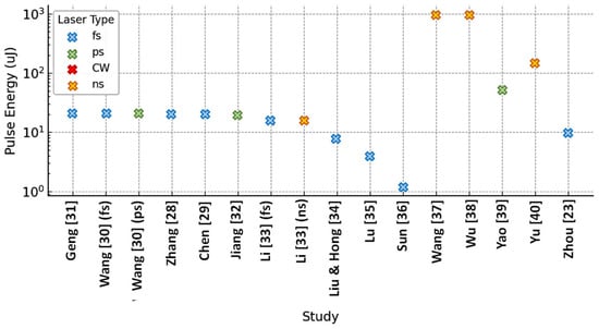
Figure 14.
The studies used various pulse energies [23,28,29,30,31,32,33,34,35,36,37,38,39,40].
3.4. Effect of Scanning Speed
In terms of scanning speed, femtosecond and picosecond systems generally enable faster scanning—ranging from several hundred to several thousand micrometers per second—because of their efficient energy coupling and low heat-affected zones. Nanosecond lasers usually operate at slower scanning speeds to allow sufficient energy delivery for material interaction and to prevent damage due to overheating (Figure 15).
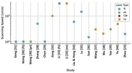
Figure 15.
The studies used various scanning speeds [23,28,29,30,31,32,33,34,35,36,37,38,39,40].
3.5. Effect of Focus Depth
Focus depth trends show that deeper focusing—up to 400 µm—is common when creating buried modified layers, especially in stealth dicing and laser exfoliation methods (Figure 16). Femtosecond lasers often require tight focusing to achieve high peak intensities in localized regions, allowing for precise control over the modification zone.
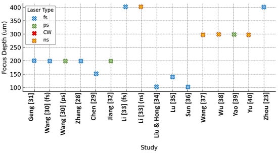
Figure 16.
The studies used various focus depths [23,28,29,30,31,32,33,34,35,36,37,38,39,40].
3.6. Effect of Track Spacing
Lastly, track spacing (or pitch) is another critical parameter. Femtosecond and picosecond lasers typically use finer spacing (as small as 2–20 µm) to maintain slicing precision and continuity of the modified layer (Figure 17). Nanosecond lasers, with their broader thermal diffusion profiles, often adopt coarser spacing, which suffices for applications that do not demand submicron accuracy.
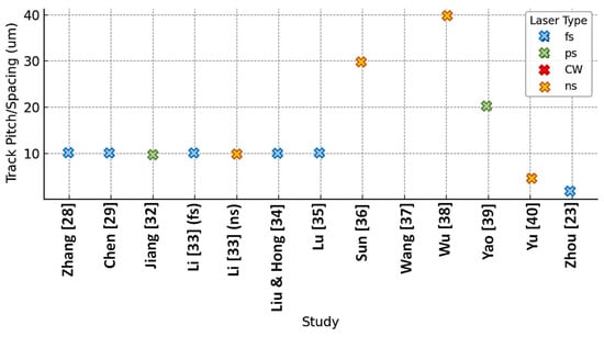
Figure 17.
The studies used various track pitches or spacing [23,28,29,32,33,34,35,36,37,38,39,40].
In summary, the optimal selection of laser parameters—pulse duration, energy, repetition rate, focus depth, scanning speed, and track spacing—depends heavily on the desired outcome, ranging from high-precision slicing to bulk material removal or structural modification in 4H-SiC. The bar chart in Figure 18 visualizes the cleaved surface roughness (Ra) from several key laser slicing studies. It compares results for monofocal vs. multifocal ultrafast laser methods, nanosecond laser slicing, and hybrid or zone-specific techniques. This helps highlight the trade-offs between surface quality and processing approaches. The surface quality achieved in various studies listed in Table 18 indicates that the wafer slicing can be quite challenging depending on the technique applied to SiC wafers.
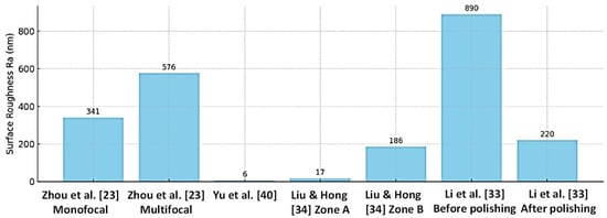
Figure 18.
The studies achieved various surface roughness of cleaved SiC wafers [23,33,34,40].
Table 18.
Cleaved surface roughness from selected studies.
The comparative visualizations generated from recent SiC laser slicing studies highlight key insights into crack dynamics, processing efficiency, and energy-material interactions. The graphics in Figure 19 illustrate the crack propagation length observed in various experimental setups. Notably, the method employed by Yao et al. [39] using a C- crystal orientation under picosecond laser irradiation achieved the longest and most controlled crack propagation (~24 µm), surpassing other configurations such as Si- and techniques reported by Wu et al. [38] and Liu & Hong et al. [34]. This suggests that optimal orientation alignment plays a critical role in enhancing cleavage behavior.
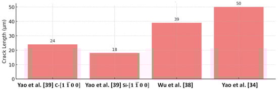
Figure 19.
The studies achieved various crack lengths during exfoliation of SiC wafers [34,38,39].
The graphic in Figure 20 compares the slicing time required for full 6-inch wafers across methods. Both Wu et al. [38] and Yu et al. [40] demonstrated high-throughput slicing using nanosecond laser processes, achieving clean separation in just 18 min. These results validate the scalability and production feasibility of crack-controlled, nanosecond-based internal modification techniques for industrial-scale wafer processing.
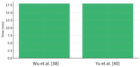
Figure 20.
The studies achieved various slicing time for SiC wafers [38,40].
Finally, the graphic in Figure 21 presents a conceptual relationship between laser power and crack depth. The trend, compiled from several studies, shows that increasing laser power correlates with deeper crack formation, indicating greater thermal stress and energy deposition within the SiC substrate. This highlights the importance of power modulation in balancing crack penetration and damage control for precise wafer separation.
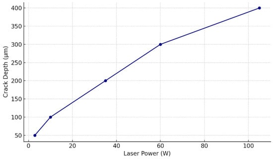
Figure 21.
The effect of laser power on obtaining crack depths for SiC wafers.
Collectively, these visual analyses underscore the influence of crystallographic orientation, pulse regime, and energy input on the efficiency and quality of SiC laser slicing processes.
4. Summary and Discussions
The most recent advances in the ultrashort pulsed laser processing of SiC wafers demonstrate significant progress in achieving high-quality slicing and exfoliation. Multi-focal picosecond laser technology [28] using 1064 nm wavelength with 1–6 focal points achieved remarkable improvements in surface quality, reducing surface roughness from 1.3 μm to 0.432 μm with 4-focal configuration and decreasing tensile strength from 22.4 MPa to 7.6 MPa for successful 6-inch 4H-SiC separation. Femtosecond ablation studies using 1035 nm lasers established critical thresholds including modification (2.35 J/cm2), transformation (4.97 J/cm2), and multi-pulse ablation (0.70 J/cm2 for 720 pulses) with an ablation depth of 22.4 nm per pulse. Picosecond stealth dicing [41] demonstrated precision processing with 1064 nm and the 30 μJ pulse energy at 100 kHz repetition rate, achieving 2 μm kerf width and 1.8 μm ± 0.12 μm surface roughness on 250 μm thick wafers (1 × 1 cm area) without residual stress. Response surface methodology analysis [33] identified laser fluence as the dominant parameter affecting groove depth, width, heat-affected zone (HAZ), and material removal rate (MRR), while scanning speed influenced depth, width, and HAZ but not MRR, and repetition rate affected depth, HAZ, and MRR. Crystal orientation studies [39] using 1064 nm picosecond lasers revealed that C-face incidence with [1–100] orientation provided optimal results with 1.79 MPa tensile strength for 6-inch n-type 4H-SiC wafers (420 μm thick), though with 120 μm damage thickness. Ultra-narrow femtosecond precision layered stealth dicing [30] using 6-pass scribing achieved exceptional precision with modified zones less than 8 μm thick, surface roughness of 224 nm Ra, successful processing of 330 μm thick 4H-SiC wafers, and an impressive aspect ratio of 9.85, highlighting the capability of femtosecond lasers for high-precision minimal-damage applications.
Summary tables on laser process parameters and their effects on processing are provided, beginning with Table 19. Specifically, laser fluence values at particular pulse widths, energy values, wavelengths, and repetition rates are listed as references with which to conduct further studies. A suggested performance metric including surface roughness, ablation threshold, modification depth, kerf width, tensile strength, and heat affected zone, together with selected studies from the reviewed literature, is presented in Table 20. Finally, the effects of the process parameters on the performance metrics are summarized in Table 21, offering guidance for researchers to further investigate and advance the field.
Table 19.
A summary table for ultrashort pulsed lasers, their parameters and effect on processing of SiC wafers as data compiled from recent literature (2022–2025).
Table 20.
The performance metrics on ultrashort pulsed laser processing of SiC.
Table 21.
The parameter effects of ultra-short pulsed laser processing of SiC on performance metrics. Legend: ↑ = Increases, ↓ = Decreases, ≈ = Minimal effect,→ = Changes character.
As indicated in the summary tables, the review identified the key insights as follows:
- (i)
- Femtosecond lasers provide higher precision with narrower modified layers and minimal thermal damage, achieving a surface roughness as low as 0.224 nm after polishing.
- (ii)
- Picosecond lasers offer higher efficiency and can achieve ultra-narrow kerf widths (<2 μm) through multiphoton-induced micro-explosions.
- (iii)
- Multi-focal techniques significantly improve surface quality (roughness reduced from 1.3 μm to 0.432 μm) and reduce tensile strength requirements.
- (iv)
- Laser fluence is the most critical parameter, affecting all performance metrics including depth, roughness, HAZ, and material removal rate.
- (v)
- Crystal orientation matters: C-face incidence with [1–100] orientation provides optimal results for n-type 4H-SiC.
- (vi)
- Multi-pulse ablation significantly reduces threshold fluence (from 4.97 to 0.70 J/cm2 with 720 pulses) due to accumulation effects.
Table 22 summarizes how key laser parameters qualitatively influence physical responses in materials. Pulse width is a primary factor, with shorter (femtosecond/picosecond) pulses minimizing melting, heat-affected zones, roughness, and cracking due to “cool” non-thermal ablation, while longer pulses increase these thermal effects. Repetition rate introduces a cumulative thermal consideration; high rates can lead to heat accumulation, potentially increasing melting and stress regardless of pulse duration. Finally, the wavelength influences the light’s absorption depth and interaction mechanism with the material, which dictates how the energy is distributed and the specific type of damage or modification that occurs.
Table 22.
Qualitative influence of laser parameters on physical material responses.
The primary limiting factors include the material’s ablation threshold, the thermal diffusion length, and the limits imposed by stress propagation.
- Ablation Threshold: This is the minimum energy density (fluence) required to remove material effectively. Processing below this threshold is inefficient, while operating significantly above it might induce undesirable side effects. The threshold depends on material properties and laser parameters like pulse duration and wavelength. This limits how efficiently a material can be processed, as simply increasing power without considering the threshold can be counterproductive.
- Thermal Diffusion Length: This parameter defines the distance heat travels within the material during the laser-material interaction time. For scalability, minimizing the HAZ is often crucial for precision. Shorter pulse durations (fs, ps) restrict heat diffusion to the interaction spot, minimizing the HAZ and thermal damage, but this requires more complex and expensive laser systems. Longer pulses (ns, CW) lead to larger thermal diffusion lengths, causing significant melting, widespread heat effects, and potential cracking, which limits the achievable resolution and quality.
- Stress Propagation Limits: Laser-generated heat and material removal induce stress and shock waves within the material. In brittle materials, e.g., SiC, these stresses can cause unwanted microcracks or bulk material failure, especially with longer pulses or high heat input. Ultrashort pulses generate less thermal stress, but rapid material expulsion can still induce shock waves that cause collateral damage. Managing these stress limits is essential for maintaining mechanical integrity and limits how quickly a process can be ramped up without compromising the final product.
These parameters collectively define the processing window for high-quality laser machining and pose significant challenges to simply increasing processing speed (scalability) without sacrificing quality.
5. Future Research Directions
This review identifies that despite significant progress; several research gaps remain in the field:
There exists lack of standardization of quality metrics. While various studies report surface roughness and chipping, there is a lack of standardized metrics and characterization methods for fully evaluating the impact of laser processing-induced defects on the long-term electrical performance and reliability of SiC-based devices.
There is a need for optimizing laser processing of SiC in the presence of crystal orientation and anisotropic properties. This review surfaces the need for more research to develop universally optimized processing parameters or adaptive control systems that can ensure uniform quality regardless of wafer orientation.
The research is needed for improving scalability and achieving industrial integration. The review reveals that much of the cutting-edge research is conducted at the lab scale. There is a gap in studies that rigorously address the challenges of scaling these technologies for high-volume, large-diameter (e.g., 200 mm) SiC wafer production while maintaining cost-effectiveness and throughput.
The research is needed to advance the current understanding of complex laser-material interaction through modeling and simulation. While some thermal and stress models exist, more comprehensive simulations are needed to predict the complex interactions between different laser parameters and SiC material properties (e.g., varying doping concentrations and wafer thicknesses) to further refine processing conditions and minimize empirical testing.
6. Conclusions
The transition from traditional silicon-based semiconductors to wide-bandgap materials such as silicon carbide (SiC) is critical for meeting the growing demands of high-power, high-frequency, and high-temperature electronic applications. However, the widespread adoption of SiC is currently constrained by challenges associated with wafer fabrication, particularly in slicing and exfoliation. Conventional mechanical techniques, such as wire sawing, suffer from substantial kerf loss, subsurface damage, and poor surface quality, which negatively impact device performance and material utilization. While ion implantation-based methods, such as smart-cut technology, offer greater control over layer transfer, they are hindered by long processing times and implantation-induced defects.
Ultrafast laser technologies, particularly femtosecond and picosecond pulsed lasers, have emerged as promising non-contact alternatives for precise and damage-minimized SiC wafer processing. Techniques like laser slicing and stealth dicing enable kerf-free exfoliation and chip separation, respectively, by generating internal damage layers with minimal thermal effects. These methods offer notable improvements in process efficiency and wafer integrity, although challenges such as surface roughness and defect accumulation remain.
Looking ahead, several important directions emerge for advancing both research and technological development in laser-based exfoliation of SiC. One key area is the optimization of laser parameters, including pulse duration, wavelength, energy density, and scanning strategies. Fine-tuning these parameters will be essential to reduce defect formation, ensure uniform slicing, and improve overall process throughput.
Another promising avenue involves hybrid processing techniques. By integrating ultrafast laser processing with complementary methods—such as smart-cut ion implantation or laser shock peening—it may be possible to achieve synergistic improvements in both efficiency and wafer quality. These hybrid approaches could overcome some of the limitations associated with standalone laser processing.
The implementation of real-time monitoring and feedback control systems represents a further step toward industrial viability. In situ diagnostics and adaptive control can significantly enhance process consistency and precision, particularly in high-throughput manufacturing settings where repeatability is critical.
Additionally, surface treatment and post-processing methods will play a crucial role in improving the final quality of exfoliated layers. Techniques for surface smoothing, cleaning, and annealing will be necessary to mitigate residual roughness and subsurface damage introduced during laser processing.
Finally, the development of material-specific process strategies will be vital. Given the anisotropic properties and defect sensitivity of SiC, tailoring laser–material interaction models to different polytypes and doping levels through advanced simulations and experimental validation will be essential to enable the development of optimized and scalable exfoliation techniques.
In conclusion, the advancement of laser-based SiC processing technologies, supported by interdisciplinary research across optics, materials science, and semiconductor engineering, has the potential to transform the cost-efficiency and scalability of next-generation electronic devices.
Author Contributions
T.Ö. Conceptualized the paper structure, collected literature, generated graphics and tables, and wrote the draft and final manuscripts. F.D.I. collected some literature initially and created a short literature review. F.D.I. participated in this study during his master’s degree at Industrial Engineering at Rutgers University- New Brunswick. T.Ö. supervised the project, including guiding data analysis, and securing project resources. All authors read and approved of the final manuscript. All authors have read and agreed to the published version of the manuscript.
Funding
This research was initially supported by the U.S. National Science Foundation (NSF-CMMI-1144637), which also inspired part of this review. Faik Derya Ince was supported as teaching assistant by Rutgers University Industrial and Systems Engineering Department.
Data Availability Statement
The data presented in this study are available on request from the corresponding author.
Acknowledgments
During the preparation of this work the author used AI-assisted technologies in order to improve language and readability with caution. After using this tool, the author reviewed and edited the content as needed and takes full responsibility for the content of the publication.
Conflicts of Interest
The authors declare no competing interests.
References
- Alves, L.F.S.; Gomes, R.C.M.; Lefranc, P.; Pegado, R.A.; Jeannin, P.O.; Luciano, B.A.; Rocha, F.V. SiC power devices in power electronics: An overview. In Proceedings of the 2017 Brazilian Power Electronics Conference (COBEP), Juiz de Fora, Brazil, 19–22 November 2017; IEEE Xplore: New York, NY, USA, 2018; pp. 1–6. [Google Scholar] [CrossRef]
- Ou, H.; Shi, X.; Lu, Y.; Kollmuss, M.; Steiner, J.; Tabouret, V.; Syväjärvi, M.; Wellmann, P.; Chaussende, D. Novel photonic applications of silicon carbide. Materials 2023, 16, 1014. [Google Scholar] [CrossRef] [PubMed]
- Zolper, J.C.; Skowronski, M. Advances in silicon carbide electronics. MRS Bull. 2005, 30, 273–275. [Google Scholar] [CrossRef]
- Cooper, J.A.; Tamaki, T.; Walden, G.G.; Sui, Y.; Wang, S.R.; Wang, X. Power MOSFETs, IGBTs, and thyristors in SiC: Optimization, experimental results, and theoretical performance. In Proceedings of the IEDM-09 Technical Digest, Baltimore, MD, USA, 7–9 December 2009; pp. 149–152. [Google Scholar]
- Jenny, J.R.; Malta, D.P.; Calus, M.R.; Müller, S.G.; Powell, A.R.; Tsvetkov, V.F.; McD Hobgood, H.; Glass, R.C.; Carter, C.H., Jr. Development of large diameter high-purity semi-insulating 4H-SiC wafers for microwave devices. Mater. Sci. Forum 2004, 457, 35–40. [Google Scholar] [CrossRef]
- Monroy, E.; Omnès, F.; Calle, F. Wide-bandgap semiconductor ultraviolet photodetectors. Semicond. Sci. Technol. 2003, 18, R33–R51. [Google Scholar] [CrossRef]
- Ivanov, A.M.; Mynbaeva, M.G.; Sadokhin, A.V.; Strokan, N.B.; Lebedev, A.A. Impact ionization in 4H-SiC nuclear radiation detectors. Mater. Sci. Forum 2010, 645–648, 1077–1080. [Google Scholar] [CrossRef]
- Cimalla, V.; Pezoldt, J.; Ambacher, O. Group III nitride and SiC based MEMS and NEMS: Materials properties, technology and applications. J. Phys. D Appl. Phys. 2007, 40, 6386–6434. [Google Scholar] [CrossRef]
- Patil, A.; Fu, X.; Mehregany, M.; Garverick, S. Fully-integrated 6H-SiC JFET amplifiers for high-temperature sensing. Mater. Sci. Forum 2010, 645–648, 1107–1110. [Google Scholar] [CrossRef]
- Kim, E.; Shimotsuma, Y.; Sakakura, M.; Miura, K. 4H-SiC wafer slicing by using femtosecond laser double-pulses. Opt. Mater. Express 2017, 7, 2450–2460. [Google Scholar] [CrossRef]
- Bidiville, A.; Wasmer, K.; Van der Meer, M.; Ballif, C. Wire-sawing processes: Parametrical study and modeling. Sol. Energy Mater. Sol. Cells 2015, 132, 392–402. [Google Scholar] [CrossRef]
- Gao, Y.; Chen, Y.; Ge, P.; Zhang, L.; Bi, W. Study on the subsurface microcrack damage depth in electroplated diamond wire saw slicing SiC crystal. Ceram. Int. 2018, 44, 22927–22934. [Google Scholar] [CrossRef]
- Gao, Y.; Chen, Y. Sawing stress of SiC single crystal with void defect in diamond wire saw slicing. Int. J. Adv. Manuf. Technol. 2019, 103, 1019–1031. [Google Scholar] [CrossRef]
- Pogue, V.; Melkote, S.N.; Danyluk, S. Residual stresses in multi-crystalline silicon photovoltaic wafers due to casting and wire sawing. Mater. Sci. Semicond. Process. 2018, 75, 173–182. [Google Scholar] [CrossRef]
- Amarasinghe, V.P.; Wielunski, L.; Barcz, A.; Feldman, L.C.; Celler, G.K. Properties of H+ implanted 4H-SiC as related to exfoliation of thin crystalline films. ECS J. Solid State Sci. Technol. 2014, 3, P37–P42. [Google Scholar] [CrossRef]
- Lee, J.; Bargatin, I.; Park, J.; Milaninia, K.M.; Theogarajan, L.S.; Sinclair, R.; Howe, R.T. Smart-cut layer transfer of single-crystal SiC using spin-on-glass. J. Vac. Sci. Technol. B 2012, 30, 042001. [Google Scholar] [CrossRef]
- Zhang, L.; Li, B.S. Study of surface exfoliation on 6H-SiC induced by H2+ implantation. Phys. B Condens. Matter 2017, 508, 104–111. [Google Scholar] [CrossRef]
- Özel, T.; Thepsonthi, T.; Amarasinghe, V.; Celler, G.K. Pulsed laser assisted exfoliation of hydrogen ion implanted single crystalline SiC thin layers. In Proceedings of the 41st North American Manufacturing Research Conference, Madison, WI, USA, 10–14 June 2013. [Google Scholar]
- Özel, T.; Thepsonthi, T.; Amarasinghe, V.P.; Celler, G.K. Nanosecond Pulsed Laser Processing of Ion Implanted Single Crystal Silicon Carbide Thin Layers. Phys. Procedia 2014, 56, 933–943. [Google Scholar] [CrossRef]
- Zhang, Y.; Liu, Z.; Tadjer, M.J.; Sun, M.; Piedra, D.; Hatem, C.; Anderson, T.J.; Luna, L.E.; Nath, A.; Koehler, A.D.; et al. Vertical GaN junction barrier Schottky rectifiers by selective ion implantation. IEEE Electron Device Lett. 2017, 38, 1097–1100. [Google Scholar] [CrossRef]
- Wang, J.; Song, Y.; Dong, B.; Zhao, Y.; Sun, Q.; Yan, M.; Yao, C.; Du, Q.; Xu, Z. Femtosecond laser controllable annealing for color centers based on ion-implanted silicon carbide substrate. Ceram. Int. 2024, 50, 46566–46578. [Google Scholar] [CrossRef]
- Yang, B.; Wang, H.; Peng, S.; Cao, Q. Precision layered stealth dicing of SiC wafers by ultrafast lasers. Micromachines 2022, 13, 1011. [Google Scholar] [CrossRef] [PubMed]
- Zhou, Y.; Liu, F.; Cao, S.; Liang, R.; Zhang, Y. Modulation of ultrafast laser-induced modified structure inside silicon carbide for thin wafer dicing. Mater. Sci. Semicond. Process. 2024, 182, 108730. [Google Scholar] [CrossRef]
- Hirata, K.; Klotzbach, U.; Washio, K.; Kling, R. New laser slicing technology named KABRA process enables high speed and high efficiency SiC slicing. In Proceedings of the SPIE Advanced Lithography, San Francisco, CA, USA, 19 February 2018; Volume 10520, p. 1052003. [Google Scholar]
- Ohmura, E.; Kumagai, M.; Nakano, M.; Kuno, K.; Fukumitsu, K.; Morita, H. Analysis of processing mechanism in stealth dicing of ultra thin silicon wafer. J. Adv. Mech. Des. Syst. Manuf. 2008, 2, 540–549. [Google Scholar] [CrossRef]
- Biard, H.; Odoul, S.; Schwarzenbach, W.; Radu, I.; Maleville, C.; Potier, A.; Ferrato, M.; Guajioty, E. Tailored polycrystalline substrate for SmartSiC™ substrates enabling high performance power devices. Solid State Phenom. 2023, 344, 47–52. [Google Scholar] [CrossRef]
- You, G.; Lin, H.; Qu, Y.; Hao, J.; You, S.; Li, B. Investigation of Exfoliation Efficiency of 6H-SiC Implanted Sequentially with He+ and H2+ Ions. Materials 2022, 15, 2941. [Google Scholar] [CrossRef]
- Zhang, Y.; Xie, X.; Huang, Y.; Hu, W.; Long, J. Internal modified structure of silicon carbide prepared by ultrafast laser for wafer slicing. Ceram. Int. 2023, 49, 5249–5260. [Google Scholar] [CrossRef]
- Chen, Q.; Yao, Y.; Zhang, J.; Li, B.; Che, L.; Zhang, X.; Fan, H.; Tian, J.; Peng, Y.; Xie, X.; et al. Effect of nitrogen doping concentration on 4H-SiC laser slicing. J. Am. Ceram. Soc. 2025, 108, e20555. [Google Scholar] [CrossRef]
- Wang, L.; Zhang, C.; Liu, F.; Zheng, H.; Cheng, G.J. Ultrafast pulsed laser stealth dicing of 4H-SiC wafer: Structure evolution and defect generation. J. Manuf. Process. 2022, 81, 562–570. [Google Scholar] [CrossRef]
- Geng, W.; Shao, Q.; Pei, Y.; Xu, L.; Cui, C.; Pi, X.; Yang, D.; Wang, R. Slicing of 4H-SiC wafers combining ultrafast laser irradiation and bandgap-selective photo-electrochemical exfoliation. Adv. Mater. Interfaces 2023, 10, 2300200. [Google Scholar] [CrossRef]
- Jiang, L.; Zhao, S.; Han, S.; Liang, H.; Du, J.; Yu, H.; Lin, X. CW laser-assisted splitting of SiC wafer based on modified layer by picosecond laser. Opt. Laser Technol. 2024, 174, 110700. [Google Scholar] [CrossRef]
- Li, Y.; Zhang, Z.; Song, Q.; Shi, H.; Hou, Y.; Yue, S.; Wang, R.; Cai, S.; Zhang, Z. Surface micromorphology and nanostructures evolution in hybrid laser processes of slicing and polishing single crystal 4H-SiC. J. Mater. Sci. Technol. 2024, 184, 235–244. [Google Scholar] [CrossRef]
- Liu, X.; Hong, M. Micro-cracks generation and growth manipulation by all-laser processing for low kerf-loss and high surface quality SiC slicing. Opt. Express 2024, 32, 38758–38767. [Google Scholar] [CrossRef]
- Lu, X.; Zhao, S.; Du, J.; Jiang, L.; Han, S.; Yu, H.; Li, X.; Lin, X. Laser double-layer slicing of SiC wafers by using axial dual-focus. Opt. Express 2025, 33, 9775–9789789. [Google Scholar] [CrossRef]
- Sun, M.; Zhao, S.; Du, J.; Han, S.; Jiang, L.; Lin, X.; Wang, X. Polarization dependences of the laser in 4H-SiC wafer slicing. Opt. Express 2025, 33, 20682–20698. [Google Scholar] [CrossRef]
- Wang, H.; Cao, Q.; Wu, T.; Wang, Z.; Hou, Y.; Peng, S.; Wang, D. Experimental investigation on crack evolution and separation strength in 4H-SiC slicing by sub-nanosecond laser. Opt. Laser Technol. 2025, 187, 112826. [Google Scholar] [CrossRef]
- Wu, W.; Yu, X.; Li, B.; Xiu, X.; Zheng, Y.; Zhang, R. Stress and crack dynamics in nanosecond laser slicing of silicon carbide. Appl. Surf. Sci. 2025, 697, 163052. [Google Scholar] [CrossRef]
- Yao, Y.; Chen, Q.; Li, B.; Zhang, J.; Wang, R.; Bai, M.; Liang, R.; Ma, L.; Ma, T.; Zhang, J.; et al. Influence of crystal orientation and incident plane on n-type 4H-SiC wafer slicing by using picosecond laser. Opt. Laser Technol. 2025, 182, 112174. [Google Scholar] [CrossRef]
- Yu, X.; Wu, W.; Li, B.; Xiu, X.; Zheng, Y.; Zhang, R. Crack control for efficient nanosecond-laser slicing of large-size 4H-SiC crystals. Appl. Surf. Sci. 2025, 697, 163014. [Google Scholar] [CrossRef]
- Han, L.; Wang, Q.; Ma, C.; Gu, B.; Li, X.; Wei, W. Research on the formation and evolution mechanism of cracks in laser stealth dicing of silicon carbide crystals. J. Mol. Graph. Model. 2024, 132, 108830. [Google Scholar] [CrossRef]
- Liu, X.; Hong, M. Heat-assisted pulsed laser processing induced nano-cracks for low kerf-loss and high-surface quality SiC wafer slicing. Opt. Laser Technol. 2025, 189, 113040. [Google Scholar] [CrossRef]
- Rehman, Z.U.; Nguyen, V.H.; Janulewicz, K.A. Ultrafast expansion kinetics of femtosecond laser-induced optical breakdown in bulk fused silica. J. Phys. D Appl. Phys. 2025, 58, 135307. [Google Scholar] [CrossRef]
Disclaimer/Publisher’s Note: The statements, opinions and data contained in all publications are solely those of the individual author(s) and contributor(s) and not of MDPI and/or the editor(s). MDPI and/or the editor(s) disclaim responsibility for any injury to people or property resulting from any ideas, methods, instructions or products referred to in the content. |
© 2025 by the authors. Licensee MDPI, Basel, Switzerland. This article is an open access article distributed under the terms and conditions of the Creative Commons Attribution (CC BY) license.