
The Improvement of Tamm Interface State Detection by Using a Porous Layer between a Metal Nanostructured Grating and a DBR †

 , ,
, , 
Abstract
1. Introduction
2. Materials and Methods
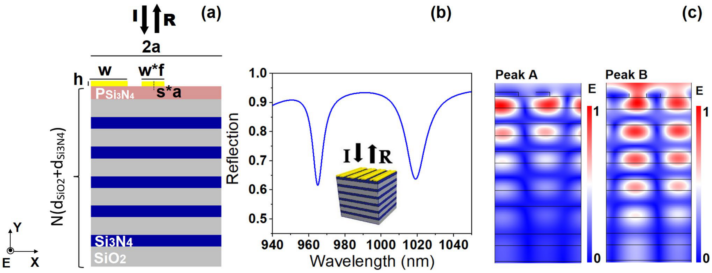
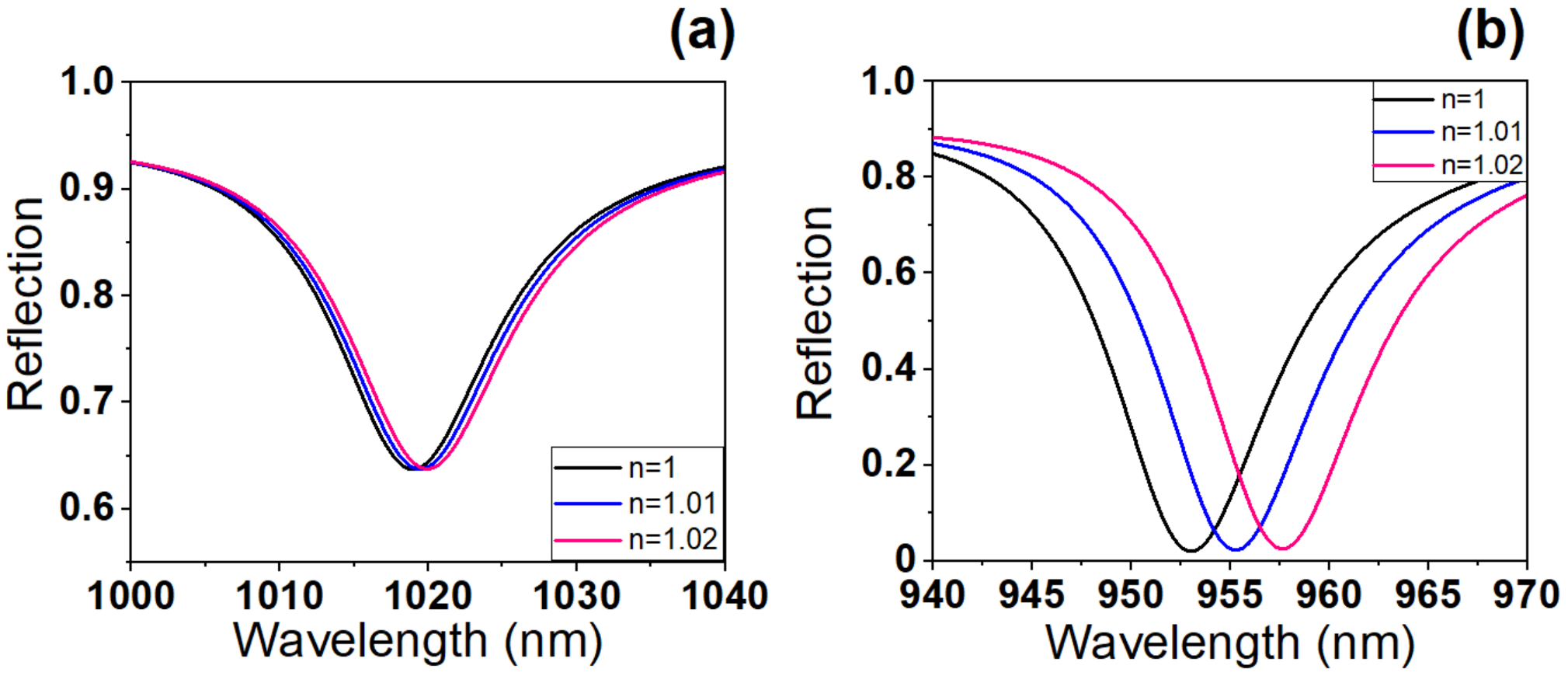
3. Results and Discussion
4. Conclusions
Author Contributions
Funding
Institutional Review Board Statement
Informed Consent Statement
Data Availability Statement
Conflicts of Interest
References
- Kaliteevski, M.; Iorsh, I.; Brand, S.; Abram, R.A.; Chamberlain, J.M.; Kavokin, A.V.; Shelykh, I.A. Tamm plasmon-polaritons: Possible electromagnetic states at the interface of a metal and a dielectric bragg mirror. Phys. Rev. B 2007, 76, 165415. [Google Scholar] [CrossRef]
- Ferrier, L.; Nguyen, H.S.; Jamois, C.; Berguiga, L.; Symonds, C.; Bellessa, J.; Benyattou, T. Tamm plasmon photonic crystals: From bandgap engineering to defect cavity. APL Photonics 2019, 4, 106101. [Google Scholar] [CrossRef]
- Juneau-Fecteau, A.; Savin, R.; Boucherif, A.; Fréchette, L.G. A practical Tamm plasmon sensor based on porous Si. AIP Adv. 2021, 11, 065305. [Google Scholar] [CrossRef]
Disclaimer/Publisher’s Note: The statements, opinions and data contained in all publications are solely those of the individual author(s) and contributor(s) and not of MDPI and/or the editor(s). MDPI and/or the editor(s) disclaim responsibility for any injury to people or property resulting from any ideas, methods, instructions or products referred to in the content. |
© 2024 by the authors. Licensee MDPI, Basel, Switzerland. This article is an open access article distributed under the terms and conditions of the Creative Commons Attribution (CC BY) license (https://creativecommons.org/licenses/by/4.0/).
Share and Cite
Haidar, O.; Mathmann, B.; Dusch, Y.; El Barghouti, M.; Lévêque, G.; Akjouj, A.; Mir, A.; Talbi, A. The Improvement of Tamm Interface State Detection by Using a Porous Layer between a Metal Nanostructured Grating and a DBR. Proceedings 2024, 97, 136. https://doi.org/10.3390/proceedings2024097136
Haidar O, Mathmann B, Dusch Y, El Barghouti M, Lévêque G, Akjouj A, Mir A, Talbi A. The Improvement of Tamm Interface State Detection by Using a Porous Layer between a Metal Nanostructured Grating and a DBR. Proceedings. 2024; 97(1):136. https://doi.org/10.3390/proceedings2024097136
Chicago/Turabian StyleHaidar, Oumaima, Baptiste Mathmann, Yannick Dusch, Mohamed El Barghouti, Gaëtan Lévêque, Abdellatif Akjouj, Abdellah Mir, and Abdelkrim Talbi. 2024. "The Improvement of Tamm Interface State Detection by Using a Porous Layer between a Metal Nanostructured Grating and a DBR" Proceedings 97, no. 1: 136. https://doi.org/10.3390/proceedings2024097136
APA StyleHaidar, O., Mathmann, B., Dusch, Y., El Barghouti, M., Lévêque, G., Akjouj, A., Mir, A., & Talbi, A. (2024). The Improvement of Tamm Interface State Detection by Using a Porous Layer between a Metal Nanostructured Grating and a DBR. Proceedings, 97(1), 136. https://doi.org/10.3390/proceedings2024097136