Abstract
Direct Laser Interference Patterning (DLIP) technique has been used to generate a line pattern on the surface of WO3 thin films, due to the interference of two coherent laser beams, modifying its surface morphology and physical properties. Gas sensing devices based on WO3 thin films annealed at 600 °C and nanostructured by DLIP have been fabricated and compared to samples simply annealed at the same temperature. The sensors processed by DLIP present a great enhancement on the response in NO2 atmospheres indicating possible modifications on the composition, aside from the morphological one.
1. Introduction
WO3 is a transition metal oxide with interesting characteristics as a gas sensing material. It presents electrochromic, photochromic and gasochromic properties and it has been used in solar cells, optical devices, gas and temperature sensors [1].
DLIP is a one step and automatable technique able to generate submicrometric structures without the need of a mask [2]. The main advantage is that the process is fast, repeatable and can be implemented at wafer level. This method has been previously investigated in other materials like metals [3] or other semiconductors such as ZnO [2,4], but it has never been used to tune intrinsic characteristics for an enhancement of the sensitivity on gas sensing applications. From previously published work about WO3 processed by three and four beam DLIP [5], innovative properties have been shown, indicating a possible application on the sensing field.
2. Materials and Methods
WO3 thin films are deposited on Pt interdigitated electrodes by RF reactive magnetron sputtering with a metal oxide target of 99.999% purity. The sputtering process is performed at 300 W of RF power in a mixed atmosphere of oxygen (40%) and argon (60%). At the back side of the sensing device, a Pt resistance is used as a heater to reach working temperatures between 200 °C and 400 °C. Finally, the sensor device is thermally stabilized in a quartz oven at 600 °C during 4 h in synthetic air.
Afterwards, some samples are processed by 2-beam DLIP setup with a tripled Q-switched Nd:YAG laser source provided by Thales, the Saga HP model (with a wavelength of 355 nm and a pulse duration of 8 ns). The optimal fluence to obtain 1D interference patterns on the surface is 50 mJ/cm2. On the setup, an optical beam splitter divides the laser source into two different beams, afterwards they are reflected in mirrors and finally addressed towards the sample surface with the same incident angle.
Atomic Force Microscope (AFM) images were taken with a JPK Nanowizard 3 AFM in Tapping Mode. The cantilevers used were Tap300-G with a resonance frequency around 300 kHz.
The gas test is carried out inside a cylindrical aluminum chamber. At the center of the chamber, there is a gas diffuser, so the gas is uniformly distributed and all the sensors receive it at the same time. For the data acquisition, a multimeter K2000 (Keithley) is used and controlled by Labview©.
In this work, the response of the devices, SR, for the oxidizing gas NO2, is defined as:

where Rair is the resistance of the sensor in air, and Rgas is the resistance in the presence of gas. The recovery time, t10, is defined as the time taken for the sensor to drop 10% of its maximum response when it is in the presence of gas and then placed in the clean air.
3. Results
As can be appreciated in Figure 1a, thermal annealed WO3 at 600 °C presents a flat surface with a roughness around 7 nm. By contrast, when the sample is processed by DLIP with a fluence of 50 mJ/cm2, a hole structure appears in a periodic line-pattern (Figure 1b,d). The holes have an average depth of 16 nm. This morphology indicates that the hole area is where higher intensity has been accumulated and consequently a higher temperature has been reached, melting and removing the material. Precisely, the higher area around the holes (Figure 1c) seems the melted WO3 removed from inside the cavities.
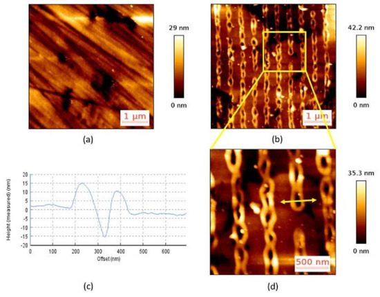
Figure 1.
AFM tapping mode images of WO3 thin film (a) annealed at 600 °C; (b) annealed at 600 °C and processed by DLIP at 50 mJ/cm2. (c) Section profile of the line point out in (d); (d) zoomed image of the sample annealed at 600 °C and processed by DLIP at 50 mJ/cm2.
In Figure 2, the response obtained by entering pulses of 2, 1 and 0.5 ppm of NO2 in the test chamber with the sensors at the optimal working temperature (~200 °C) has been plotted. As shown, sensors processed by DLIP present an enhance in the response for all the tested concentrations. The morphological properties of the material have been modified and as shown in Figure 2, there is an influence on the NO2 detection mechanism.
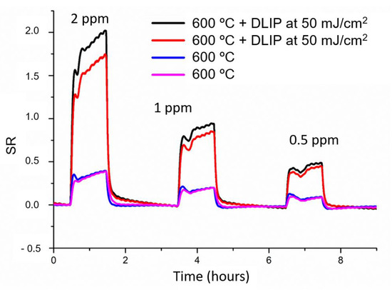
Figure 2.
Pulses of 2, 1 and 0.5 ppm of NO2 for WO3 thin film sensors annealed at 600 °C, processed and non-processed by DLIP at 50 mJ/cm2.
A summary of the sensor responses and response times is shown in Figure 3. While in sensors nonprocessed by DLIP (A7 and C1) the recovery time always increases with the NO2 concentration, the sensors processed by DLIP (C3 and C4) have a minimum t10 (~8.2 min) for the higher concentration (2 ppm).
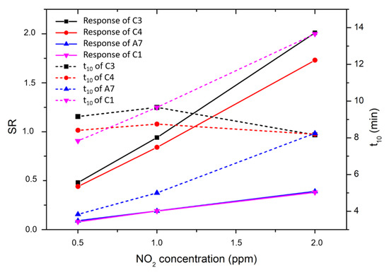
Figure 3.
Sensor responses and recovery time (t10) for three different concentrations of NO2, both for sensors processed by DLIP at 50 mJ/cm2 (C3 and C4) and non-processed (A7 and C1).
4. Conclusions
WO3 thin films, annealed at 600 °C and processed by DLIP at 50 mJ/cm2 show 1D patterns with hole structures where the highest intensity of the laser has heated the sample. This technique has increased the roughness and surface-to-volume ratio compared to only annealed samples.
The sensor devices processed by DLIP at 50 mJ/cm2 have shown excellent sensing properties for low concentrations of NO2 (2, 1 and 0.5 ppm). These results could be explain by the modification of the composition due to the high temperatures reached at the sample, as shown in previous work [4], generating holes and melt structures.
Author Contributions
I.C.-H. and G.G.M. conceived and designed the experiments; L.P.-M. and M.M.-C. performed the experiments; L.P.-M. and S.M.O. analyzed the data; G.Z., S.G. and C.M. contributed reagents/materials/analysis tools; L.P.-M. and G.G.M. wrote the paper.
Acknowledgments
This work was supported by the Ministry of Economy and Competitiveness (MINECO) through the TEMIN-AIR+ (project n° TEC206-79898-C6-3-R) and by the Basque Government under the Elkartek program (MICRO4FAB grant n° KK-2016-00030). The authors also wish to thank SCENT s.r.l. for financing this research.
Conflicts of Interest
The authors declare no conflict of interest. The founding sponsors had no role in the design of the study; in the collection, analyses, or interpretation of data; in the writing of the manuscript, and in the decision to publish the results.
References
- Wang, Y.-D.; Chen, Z.-X.; Li, Y.-F.; Zhou, Z.-L.; Wu, X.-H. Electrical and gas-sensing properties of WO3 semiconductor material. Solid State Electron. 2001, 45, 639–644. [Google Scholar] [CrossRef]
- Berger, J.; Roch, T.; Correia, S.; Eberhardt, J.; Lasagni, A.F. Controlling the optical performance of transparent conducting oxides using direct laser interference patterning. Thin Solid Films 2016, 612, 342–349. [Google Scholar] [CrossRef]
- Bieda, M.; Siebold, M.; Lasagni, A.F. Fabrication of sub-micron surface structures on copper, stainless steel and titanium using picosecond laser interference patterning. Appl. Surf. Sci. 2016, 387, 175–182. [Google Scholar] [CrossRef]
- Parellada-Monreal, L.; Castro-Hurtado, I.; Martínez-Calderón, M.; Rodriguez, A.; Olaizola, S.M.; Gamarra, D.; Lozano, J.; Mandayo, G.G. Study of sputtered ZnO modified by Direct Laser Interference Patterning: Structural characterization and temperature simulation. Appl. Surf. Sci. 2018, 441, 331–340. [Google Scholar] [CrossRef]
- Castro-Hurtado, I.; Tavera, T.; Yurrita, P.; Pérez, N.; Rodriguez, A.; Mandayo, G.G.; Castaño, E. Structural and optical properties of WO3 sputtered thin films nanostructured by laser interference lithography. Appl. Surf. Sci. 2013, 276, 229–235. [Google Scholar] [CrossRef]
Publisher’s Note: MDPI stays neutral with regard to jurisdictional claims in published maps and institutional affiliations. |
© 2018 by the authors. Licensee MDPI, Basel, Switzerland. This article is an open access article distributed under the terms and conditions of the Creative Commons Attribution (CC BY) license (https://creativecommons.org/licenses/by/4.0/).