Abstract
This paper presents for the first time, the integration of ultra-thin (<10 nm) atomic layer deposition (ALD) aluminum oxide (Al2O3) membranes as electron transparent windows (ETWs) for transmission electron microscope (TEM) nanoreactor applications. The process was successfully implemented and tested in a TEM. ETWs with thicknesses down to 5 and 10 nm were used to image nanoparticles (NPs) in a 120 keV TEM and 200 keV TEM respectively.
1. Introduction
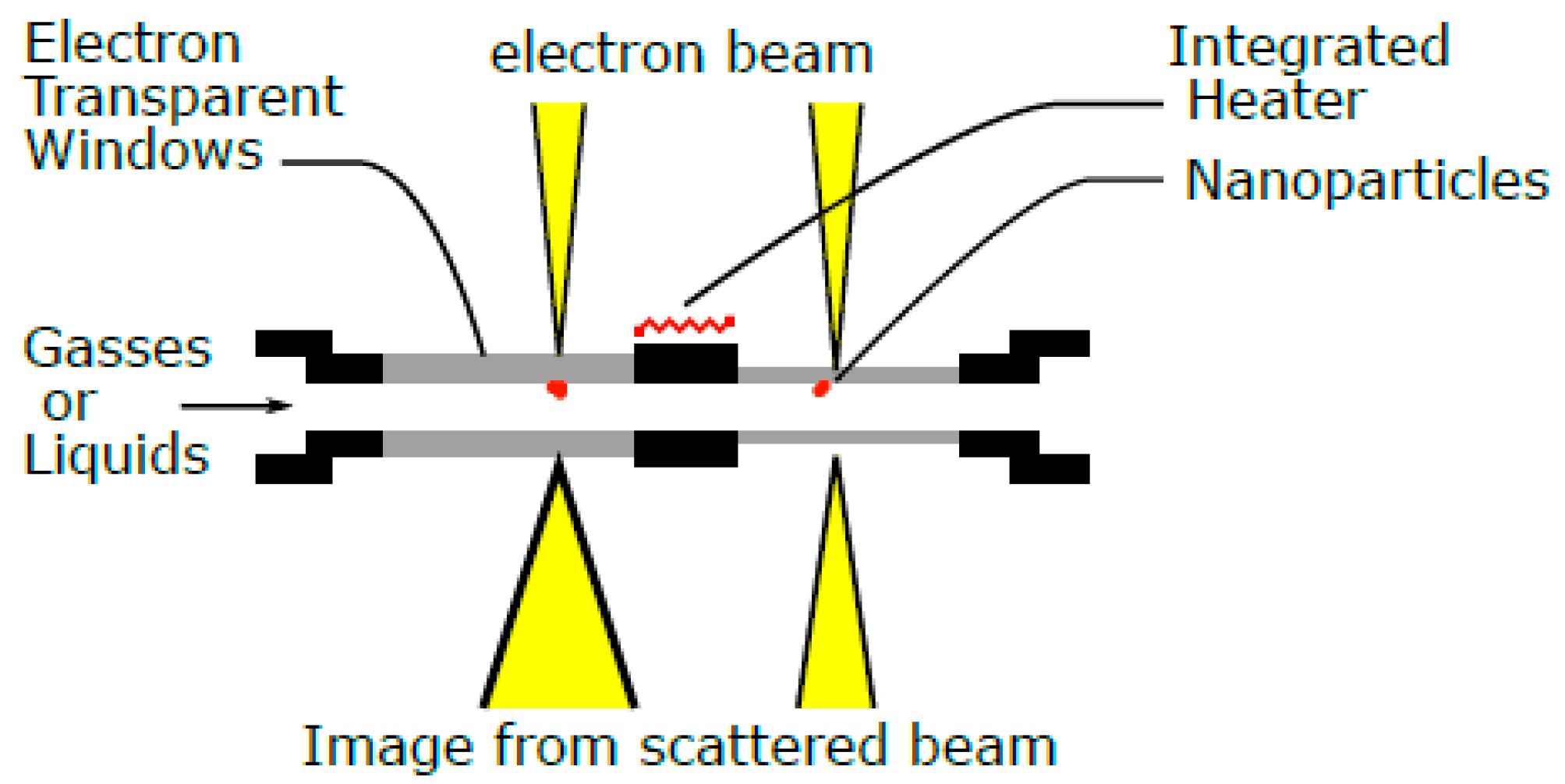
MEMS nanoreactors are devices that allow scientists to study nanocatalysis in-situ (during the reaction) in a TEM, while also controlling the pressure and temperature of the reaction [1,2]. ETWs are ultra-thin membranes that allow the transmission of the electron beam with a minimal amount of scattering. NPs are deposited onto the ETWs, and studied in a TEM at high resolution. Reducing the electron beam scattering in the ETW is critical in obtaining higher resolution NPs images [3]. To increase the resolution for TEM users, the scattering must be minimized with respect to the NP they wish to image to form the clearest possible background. The most effective way to minimize the scattering is to reduce the thickness of the ETW (Figure 1).
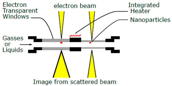
Figure 1.
Schematic view of a MEMS nanoreactor and components. Two different ETWs are illustrated here. The thicker ETW (left) scatters the electron beam more strongly, which causes a reduction of resolution compared to the thinner window on the right.
Current ETW materials have provided good image quality for thicker and heavier NPs, however contrast issues arise in experiments when lighter NPs need to be studied. State-of-the-art ETWs commercially available are 20–30 nm thick and are integrated in nanoreactors that can withstand 1 bar pressure [4]. This paper presents ultra-thin (<10 nm) ALD ETWs, which were successfully integrated in a TEM nanoreactor and tested.
2. Materials and Methods
2.1. Material and Deposition Selection
Current ETWs are deposited by low pressure chemical vapor deposition (LPCVD), a technique which can produce the desired qualities of ETWs (uniformity, continuity) however only down to a thickness of 15 nm. In contrast, ALD can keep these qualities for ultra-thin layers (down to a few nanometers) and can be deposited at much lower temperatures (T < 300 °C, even under 100 °C), 27 significantly reducing the thermal budget of the process. In this paper Al2O3 was selected as the ALD material due to its comparable mass density to LPCVD SiN, and its resistance to vapor hydrogen fluoride (VHF)—which allowed SiO2 to be sacrificially removed in the process.
2.2. Fabrication Process
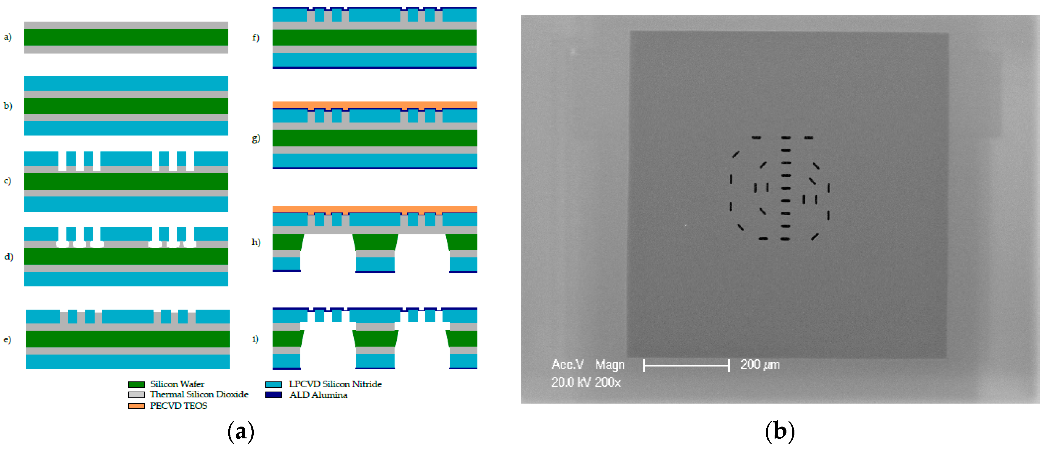
The fabrication process of the ALD Al2O3 integrated TEM nanoreactor is shown in nine steps in Figure 2. (a) 200 nm of thermal SiO2 is grown on the single-side polished <100> silicon wafer. The oxidation temperature was 1000 °C. The SiO2 is used as an etchant-stop for the (tetramethylammonium hydroxide) TMAH etch later in the process, and is used as a sacrificial layer at the end of the process. (b) 1 µm of SiN is deposited using LPCVD. The SiN will become the mechanically supporting membrane of the ETWs. (c) On the front-side, the ETW holes are dry-etched to land on the thermal SiO2. (d) The wafers are etched in BHF to remove the remaining oxide in window holes. (e) 800 nm of thermal oxide is regrown in the window holes. (f) Al2O3 is deposited via ALD at 300 °C. (g) 1 µm of PECVD TEOS is deposited on top of the Al2O3. This TEOS layer functions as a protective capping layer. (h) On the back-side, the TMAH openings are dry-etched to remove the SiN, SiO2 and Al2O3 to reveal the bare silicon. With the front-side protected by a mechanical holder, the wafer then is etched in TMAH to remove the silicon wafer. (i) Lastly, VHF is used to release TEOS and thermal SiO2.
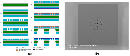
Figure 2.
(a) Process flow for Al2O3 ETWs. (b) a resulting SEM image of the device which includes the ETWs suspended in a SiN supporting membrane.
2.3. Process Results and Film Characterization
The ETWs are integrated into an 800 µm2 square-shaped SiN membrane, which is defined in Figure 2a, step h. On the membrane there are 26, 20 × 5 µm2 elongated circles. The circles are patterned in a spiral configuration, in the center of the membrane (Figure 2b).
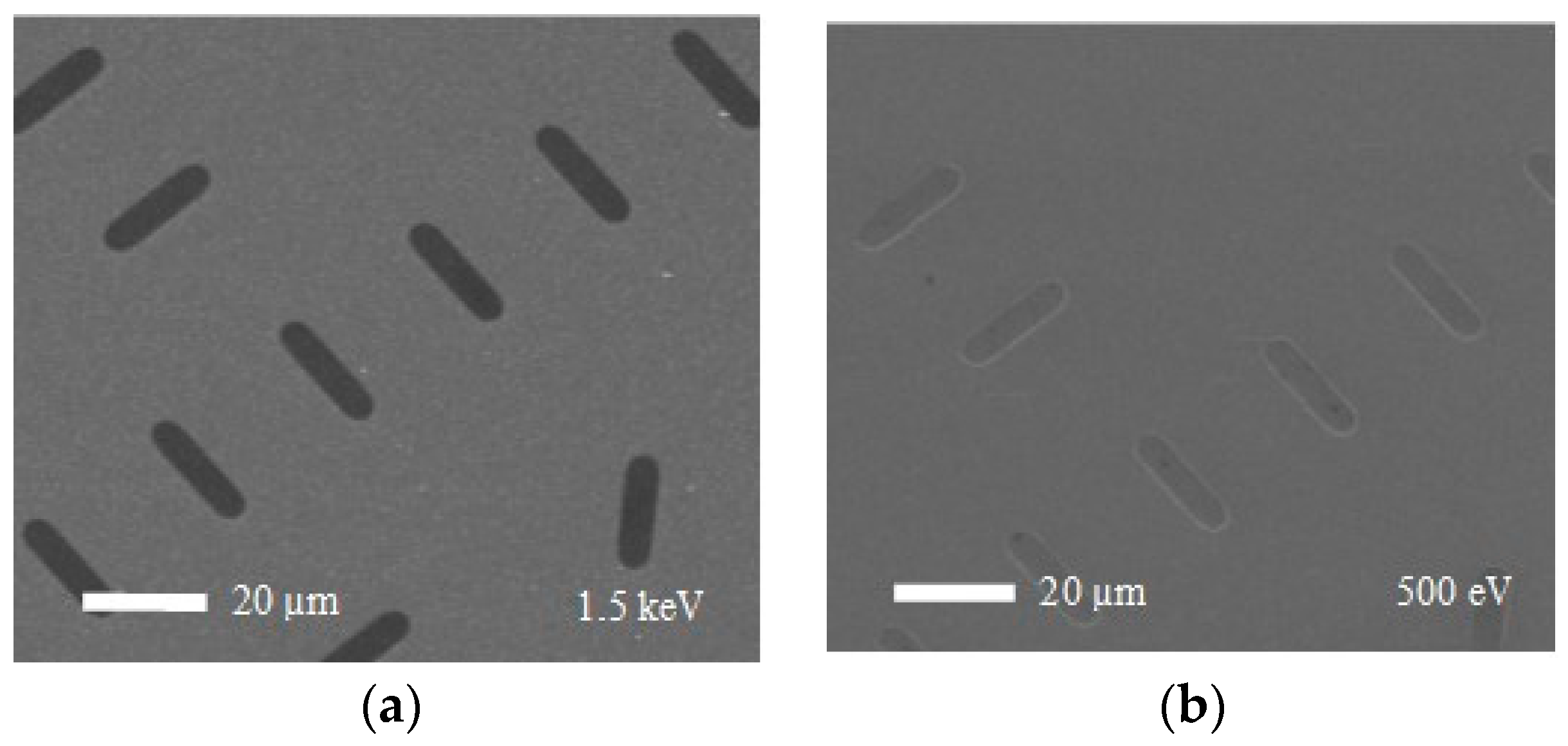
Figure 3a,b are both scanning electron microscope (SEM) images of the same device but at different electron beam energies, 1.5 keV and 500 keV respectively. At lower energies, the ETWs are indistinguishable from the SiN membrane indicating that the ETWs exist. In Figure 3a, the ETWs are completely transparent in the SEM. A finely controllable growth rate of 0.88 nm/cycle, and an ultra-smooth surface roughness of 0.3 nm were measured for the ALD Al2O3 layer.
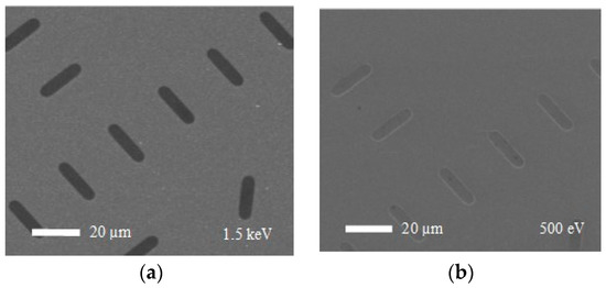
Figure 3.
SEM images taken on an identical chip, at different electron beam energies. (b) imaged at 500 eV, and (a) imaged at 1.5 keV.
3. Results and Discussion
3.1. Imaging Quality
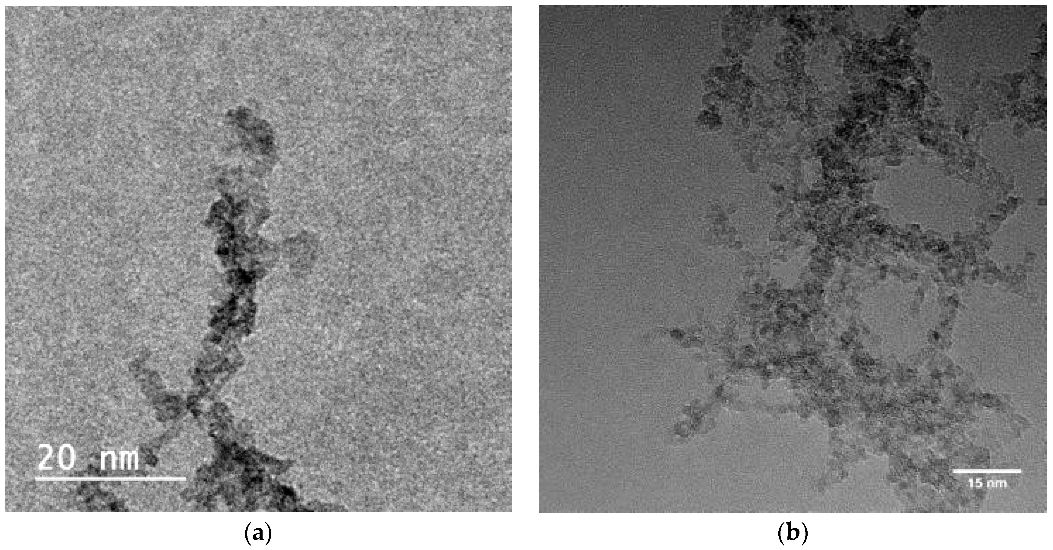
To compare the imaging quality a 5 nm Al2O3 (Figure 4a) and 20 nm SiN (Figure 4b) ETWs with nickel oxide (NiO) NPs imaged in a 120 keV and 200 keV, respectively. While the images are taken at different electron energies and slightly different magnifications, the comparison shows a considerable improvement in the clarity of the imaged NiO NPs.

Figure 4.
NiO NPs being image on: (a) 5 nm Al2O3, 120 keV TEM; (b) 15 nm SiN ETW, 200 keV TEM. (a) has a much brighter background indicating that the electron beam is minimally scattered compared to (b).
3.2. Threshold Pressure
Besides providing good imaging quality, the ETW must also withstand the pressure of the reaction inside the nanoreactor. A threshold pressure test was also performed to determine the pressure limit of the Al2O3 ETWs using a custom build setup (Figure 5). ALD Al2O3 that are 5 nm and 15 nm thick were able to withstand 0.75 and 1.25 bar respectively. While the shape of these ETWs were not optimized for pressure, this test gives an indicator of what to expect with ALD Al2O3 at these thicknesses.
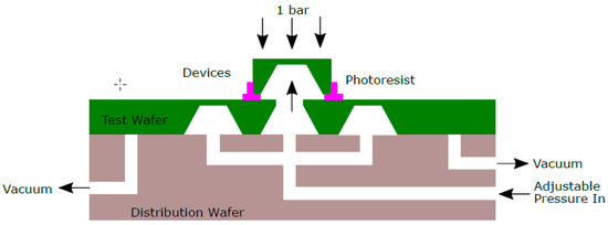
Figure 5.
A cross-sectional drawing of the set-up for the threshold pressure experiment.
4. Conclusions
In this paper, a process was successfully developed to integrate ALD Al2O3 in a MEMS nanoreactor. ETWs as thin as 5 nm were able to be used to image NPs in a 120 keV TEM. An improvement in imaging quality is evident by the brighter background in the TEM image. Additionally, the threshold pressure was tested at different thicknesses to give an indication of robustness in pressurized nanoreactor experiments. While the technique presented in this paper is focused on improving the imaging quality of nanoreactors, it may also be useful in other membrane-based applications.
Acknowledgments
The authors would like to acknowledge Maren Bremmer and Mariya Sholkina from DENS Solutions for TEM imaging, and Max Koole from VSPARTICLE for the NiO sample preparation.
Conflicts of Interest
The authors declare no conflict of interest.
References
- Creemer, J.F.; Helveg, S.; Kooyman, P.J.; Molenbroek, A.M.; Zandbergen, H.W.; Sarro, P.M. A MEMS Reactor for Atomic-Scale Microscopy of Nanomaterials Under Industrially Relevant Conditions. J. Microelectromech. Syst. 2010, 19, 254–264. [Google Scholar] [CrossRef]
- Morana, B. Silicon Carbide Thin Films for MEMS Nanoreactors for In-Situ Transmission Electron Microscopy. Ph.D. Thesis, TU Delft, Delft, The Netherlands, 2018. [Google Scholar] [CrossRef]
- Goossen, L.M. Ultra-Thin Integrated ALD Alumina Electron-Transparent Windows for Nanoreactor Applications. Master’s Thesis, TU Delft, Delft, The Netherlands, 2018. [Google Scholar]
- Dens Solutions. Available online: http://denssolutions.com/ (accessed on 1 June 2018).

Publisher’s Note: MDPI stays neutral with regard to jurisdictional claims in published maps and institutional affiliations. |
© 2018 by the authors. Licensee MDPI, Basel, Switzerland. This article is an open access article distributed under the terms and conditions of the Creative Commons Attribution (CC BY) license (https://creativecommons.org/licenses/by/4.0/).