Abstract
The state-of-the-art infrared (IR) detection uses quantum photodetectors and bolometers. Quantum IR photodetectors are expensive and require cooling, and exotic and toxic materials. Whereas, bolometers are cost-efficient and uncooled, but they are much slower and less sensitive. Recently we have demonstrated that ultra-thin, highly-doped silicon membranes can be used to build fast and highly-sensitive thermoelectric bolometers. We present the fabrication of these devices, electro-thermal characterization results, and estimate the full potential of this technology.
1. Introduction
The state-of-the-art IR detection is based on either bolometers or quantum photodetectors (i.e., photovoltaic and photoconductive detectors). Quantum IR photodetectors have high performance, but they are expensive and require cooling. Exotic and toxic materials (e.g., HgCdTe) are also needed at longer wavelengths. The bolometers are uncooled thermal detectors with lower cost. Compared to the cooled detectors they are much slower and have approximately an order of magnitude lower specific detectivity in the long-wavelength IR.
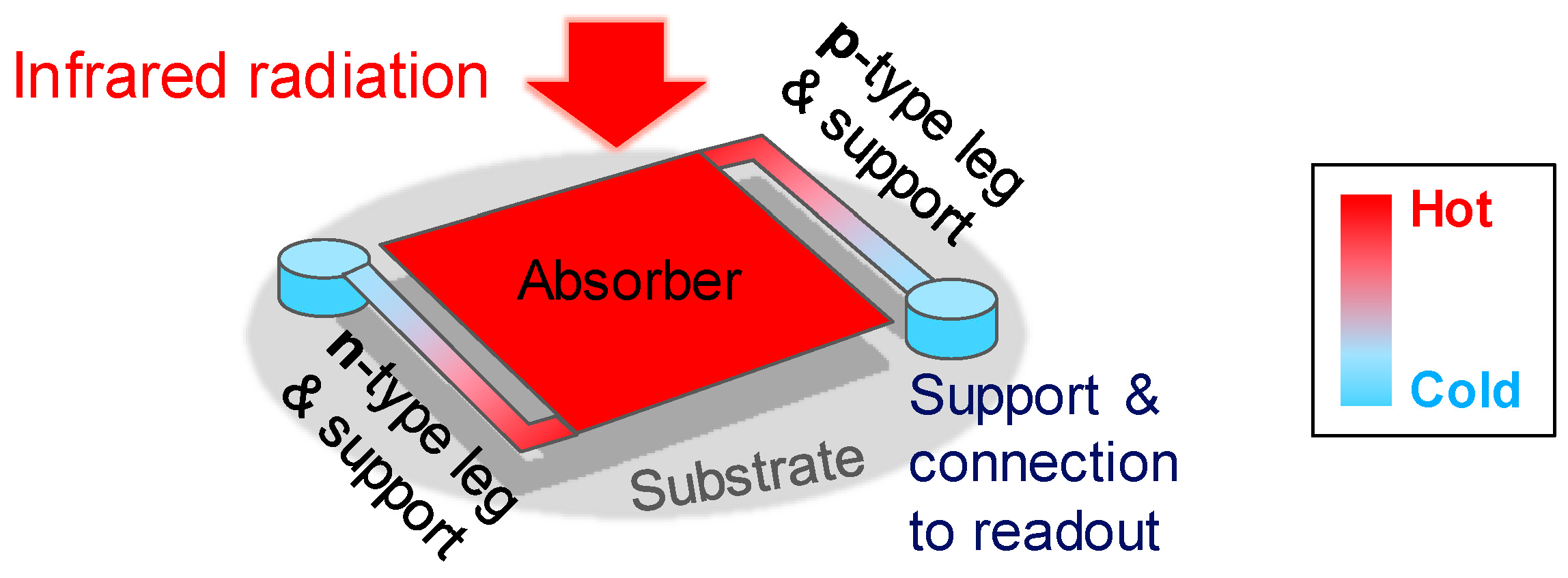
A bolometer consists of the absorber of incident radiation and a transducer, which converts the change of the temperature of the absorber into electric signal. The most common bolometers are resistive bolometers, which use temperature-dependent resistor as transducers. A thermionic bolometer sketched in Figure 1 uses thermoelectric transduction. The absorber of the bolometer is thermally isolated from the ambient and the substrate, on which the bolometer is fabricated, by vacuum. The absorber temperature changes are detected with a thermocouple or thermopile, where the Seebeck effect generates a voltage due to a thermal gradient along the supporting beams.

Figure 1.
A schematic of a thermoelectric bolometer: (i) The absorber absorbs the incident thermal radiation. (ii) The thermoelectric transducer consisting of n- and p-type legs converts the thermal signal to voltage and passes it to the readout electronics. (iii) The supporting beams support the structure and provide thermal isolation. The thermoelectric transducer can be located on/in the supporting beams or it itself can act as support as in the present nanomembrane devices.
Recently we have demonstrated that ultra-thin, highly-doped single-crystalline silicon membranes and optical thin-film absorbers can be used to build fast and highly-sensitive thermoelectric bolometers for IR detection [1,2]. The high sensitivity of this technology arises from low phonon thermal conductivity of the ultra-thin silicon membrane [3]. The estimated high speed is due to the extremely small thermal mass of the nanomembrane and the optical absorber [2].
In this work we compare the characteristics of thermoelectric thermal detector devices based on single-crystalline (SC) and polycrystalline silicon nanomembranes. Lower resistivities can be obtained with SC Si than with poly-Si, but poly-Si allows for simpler and more cost-efficient fabrication. The devices are equipped with built-in heaters for material and device characterization. The devices can also be directly used for scientific instrumentation. We present the fabrication of the devices, the characterization results, and estimate the full potential of this technology.
2. Modelling of Thermoelectric Thermal Detectors and Bolometers Based on Nanomembranes
Thermoelectric detectors can be described using a first order opto-electro-thermal model [1,2]. The output voltage of a thermoelectric thermal detector is given by [1,2]
where P is the amplitude of the power modulation from an external signal such as infrared radiation or a built-in heater, S = Sp − Sn is the total Seebeck coefficient and Sp and Sn are the Seebeck coefficients of the p and n type materials of the thermocouple(s), respectively, G is the total thermal conductance of the device, and τ is the thermal time constant of the device. The noise in these devices is dominated by the Johnson-Nyquist noise originating from the electric resistance of the thermocouple(s) R and the fundamental thermal fluctuation noise [1,2]. Below the thermal cut off (ω << τ) the noise-equivalent power (NEP) of the thermoelectric detectors can be written as [1]
where NEPth = (4kBT2G)1/2 is the NEP of the thermal fluctuation noise, kB is Boltzmann’s constant, T is the absolute temperature, and ZeffT = S2T/(GR), is the detector effective thermoelectric figure of merit. The NEP of the Johnson-Nyquist noise is given by NEPJN = (dP/dV)(4kBTR)1/2.
V = PSG−1 (1 + ω2τ2)−1/2,
NEP = NEPth[1+ 1/(ZeffT)]1/2,
3. Fabrication of Nano-Thermocouple Devices
The devices were fabricated in the VTT Micronova clean room facilities on 150 mm silicon-on-insulator (SOI) (SC devices) and standard (poly-Si devices) silicon wafers following the fabrication process described in Ref. [1]. In the beginning the SOI layer was thinned to 40 nm by thermal oxidation and oxide stripping. The poly-Si device wafers were oxidized to form a buried silicon oxide and then 100 nm of LPCVD polysilicon was deposited on them. Next, both Si layers were doped selectively with boron and phosphorus and patterned by plasma etching. Then, a 280-nm-thick stress-compensation SixNy layer was deposited by LPCVD. Next, a 30 nm thick layer of Al was then sputtered and patterned by wet etching. Finally, the devices were released by a deep reactive etching through the silicon wafer from the back side and HF vapor etching of the buried oxide layer.
4. Results and Discussion
4.1. Experimental Results
The images of the fabricated devices and their electro-thermal characteristics are shown in Figure 2. The device based on SC-Si nanomembrane is denoted by device S and the poly-Si device by device P. The characteristics of the devices are summarized in Table 1. The NEP of device S was measured and the NEP of device P was calculated by assuming that the Johnson-Nyquist noise dominates as it is the case in the device S as well.
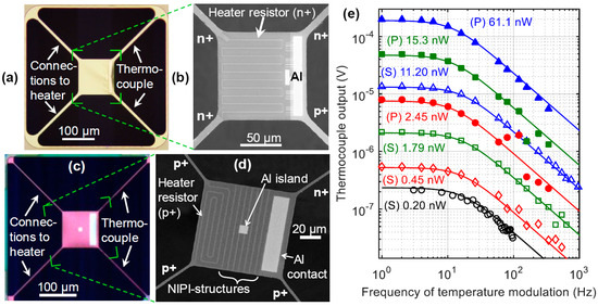
Figure 2.
(a–d) Optical (a,c) and scanning-electron (b,d) micrographs of device S (a,b) [1] and device P (c,d). The devices have a built-in electric heater for characterization and experimentation, and a thermocouple for temperature readout. The pair of the silicon beams on the left side of the devices provides the electrical connection for the meandered doped silicon heater resistor patterned in the silicon membrane. The 30 nm Al film forms an electrical contact between ends of the n+ and p+ silicon beams acting as thermocouple. Device P has an Al island for scanning probing experiments and additional n and p type doped regions (NIPI) between the heater meanders and the heater and the thermocouple in order ensure good electrical insulation between the doped active regions. However, insulation cannot affect this work because lock-in techniques are used and the excitation and readout is done at different frequencies. (e) Frequency responses of devices S [1] and P measured using lock-in techniques [1]. Symbols are the measured thermocouple output voltage amplitudes as function of the frequency of heater power amplitudes at several power values. The curves show the response [Equation (1)] fitted to the data. The fitting parameters are listed in Table 1.

Table 1.
Characteristics of device S [1] and P.
Although the devices are made of different silicon, their speed (τ) and sensitivity (NEP) are quite similar. The largest differences in responsivity dV/dP and R are explained by the differences in coefficient S and material resistivities. The properties of the nanomembranes are listed in Table 2. The poly-Si nanomembranes have higher resistivities due to lower doping and lower mobility. The lower doping gives also rise to higher value of S compared to the SC Si. Coefficient S was measured using the heater resistors of the devices as resistive thermometers and the thermocouples as Peltier cooler and heater [1]. The responsivity formula dV/dP = S/G and the value of S allows estimation of the average thermal conductivity of the nanomembranes, giving around 40 W/m/K for both SC and poly Si. Although the thickness of the poly-Si membrane is larger, the hindering effect of the grains seems to compensate for the lesser confinement of phonons responsible for thermal conduction.
Table 2.
Comparison of properties of SC [1] and polycrystalline silicon nanomembranes.
4.2. Estimated Optical Performance of Thermoelectric Bolometers Based on Silicon Nanomembranes
The fabricated devices can be converted into bolometers for optical infrared detection by replacing the built-in heaters with optical absorbers such as 10 nm Ti [2]. Based on our model [2], the optical NEPs of these devices can be estimated. The calculated result is shown in Figure 3.
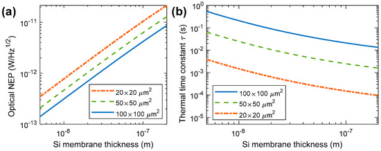
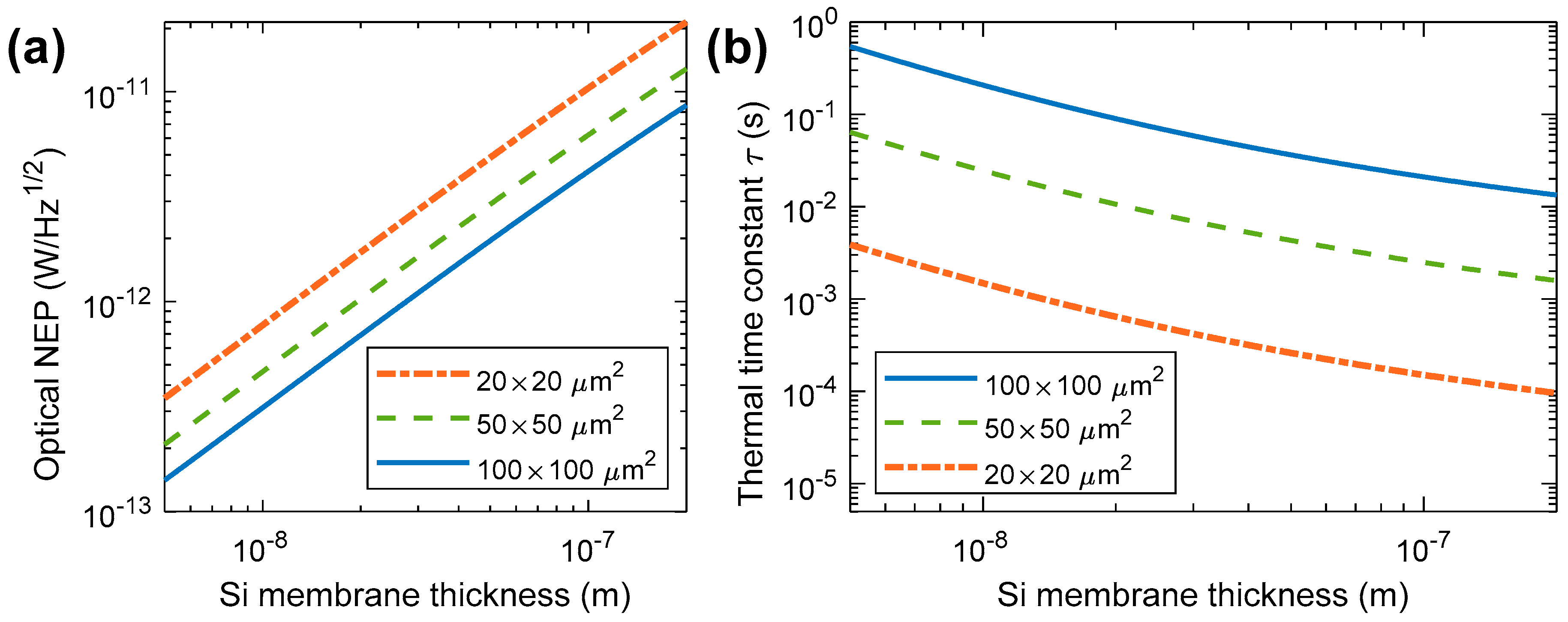
Figure 3.
Calculated (a) optical NEP and (b) thermal time constant of the thermoelectric bolometers with various sizes as functions of the silicon nanomembrane thickness [2].
Figure 3 shows that the NEP of these devices decrease remarkably when the thickness of the silicon membrane is reduced. This due to decreasing sheet thermal conductance Gsh of the nanomembrane. The dependence of τ is due to combined effects of Gsh and decreasing heat capacity [2]. Our calculations [2] show that optical NEP below 1 pW/Hz1/2 and τ in the order of 1 ms can be achieved. These values are considerably better than those of the state of the art [4]. Our calculations show [2] also that the larger detectors are limited only by the background radiation instead of the detector internal noise.
Author Contributions
M.P., J.A., A.V., A.V.T., K.T., J.H., and A.S. conceived the devices and experiments; A.V., A.V.T., A.S., K.T., and M.P. designed the devices and fabrication; K.G. and A.S. fabricated the devices; A.V., A.V.T., and M.P. designed the experiments; A.V. and A.V.T. performed the experiments; A.V., A.V.T. and M.P. analyzed the data; A.V. wrote the paper.
Acknowledgments
This work has been financially supported by the European Union Seventh Framework Programme (Grant Agreement No. 604668, project QUANTIHEAT), by European Union Future and Emerging Technologies (FET) Open under Horizon 2020 programme (Grant Agreement No. 766853, project EFINED), and by the Academy of Finland (Grant No. 295329).
Conflicts of Interest
The authors declare no conflict of interest.
References
- Varpula, A.; Timofeev, A.V.; Shchepetov, A.; Grigoras, K.; Hassel, J.; Ahopelto, J.; Ylilammi, M.; Prunnila, M. Thermoelectric thermal detectors based on ultra-thin heavily doped single-crystal silicon membranes. Appl. Phys. Lett. 2017, 110, 262101. [Google Scholar] [CrossRef]
- Varpula, A.; Timofeev, A.V.; Shchepetov, A.; Grigoras, K.; Ahopelto, J.; Prunnila, M. Thermoelectric bolometers based on silicon membranes. Proc. SPIE 2017, 10246, 102460L. [Google Scholar] [CrossRef]
- Neogi, S.; Reparaz, J.S.; Pereira, L.F.C.; Graczykowski, B.; Wagner, M.R.; Sledzinska, M.; Shchepetov, A.; Prunnila, M.; Ahopelto, J.; Sotomayor-Torres, C.M.; et al. Tuning Thermal Transport in Ultrathin Silicon Membranes by Surface Nanoscale Engineering. ACS Nano 2015, 9, 3820. [Google Scholar] [CrossRef] [PubMed]
- Dillner, U.; Kessler, E.; Meyer, H.-G. Figures of merit of thermoelectric and bolometric thermal radiation sensors. J. Sens. Sens. Syst. 2013, 2, 85. [Google Scholar] [CrossRef]
Publisher’s Note: MDPI stays neutral with regard to jurisdictional claims in published maps and institutional affiliations. |
© 2018 by the authors. Licensee MDPI, Basel, Switzerland. This article is an open access article distributed under the terms and conditions of the Creative Commons Attribution (CC BY) license (https://creativecommons.org/licenses/by/4.0/).