Abstract
Pd–anodic oxide–InP metal–oxide–semiconductor (MOS) structures are fabricated to develop a hydrogen sensor capable of effectively operating at room temperature. Through palladium amount varying the signal recovery time has been improved (became shorter). Decrease of photovoltage and strong increase of photocurrent were observed for illuminated by LED structures under hydrogen pulse exposure. The gas testing was carried out in 0.1–10% hydrogen in nitrogen, and in 100% hydrogen. As a result, low power-consumption hydrogen sensor with a fast response-recovery time 1/20 s. was developed.
1. Introduction
Currently a lot of attention is focused on the development of hydrogen sensors to register the hydrogen leaks from fuel cells, hydrogen storage as well as automobile engines. From this viewpoint, it is necessary to develop new selective to hydrogen, high-sensitive, fast and cheap gas sensors working at or near room temperature. Today in the literature there are a significant number of publications are concerned with solid state hydrogen sensors based on metal oxide films, coated a ceramic or silicon. The main disadvantages of this type of sensors are high operating temperature (300–800 °C) and low selectivity. The sensor working at high temperatures itself becomes a possible trigger of explosion, due to its enough input electrical energy of sensor operation [1]. The main advantages of Pd-contained sensors on the base of field-effect transistors, MOS structures, and structures with Schottky barrier are possibility to operate at room temperature, high selectivity to hydrogen and low-power consumption [2,3,4,5,6].
In this work the technology of sensitive element based on Pd-anodic oxide-InP structure was developed and its photoelectrical properties were studied to evaluate the influence of the thickness of Pd layer on photovoltage recovery time towards gaseous hydrogen. Earlier we studied electrical and photoelectrical properties of Pd–anodic oxide–InP structures [7,8].
2. Materials and Methods
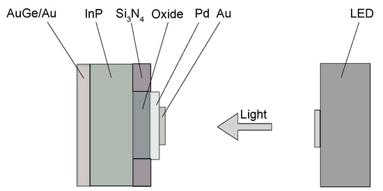
The structure under investigation is shown schematically in Figure 1. (100) InP n = 1016 cm−3 served as the substrate. Prior to the deposition of palladium, the substrate was treated with an etchant to remove surface contaminants and then oxidized by means of anodic oxidation. The thickness of the palladium layers deposited by thermal evaporation in vacuum varied within the range of 15–50 nm. To exclude the surface current leakage the chip perimeter surface area was coved by Si3N4. On the InP semiconductor substrate with oxide and palladium layers, we deposited a cross-shaped Au contact layer by thermal evaporation in vacuum to provide a uniform spread of the current over the surface. An ohmic Cr/AuGe/Au contact was formed on the back side of the InP substrate. The above Pd-Oxide-InP structure and LED with a wavelength of 0.9 µm was used in the hydrogen sensor.

Figure 1.
Scheme of optopair for the photoelectrical Hydrogen Sensor: sensitive element (Pd-anodic oxide-InP structure cross-section) and light emitting diode (λ = 0.9 μm).
3. Results and Discussion
The current-voltage characteristics of the typical Pd–oxide–n-InP structure were investigated at the temperature range from 90 to 300 K. They demonstrated the diode character and cut-off voltage depended on temperature. Schottky barrier height was determined from I to V characteristics. The barrier height of 0.55 eV is enough for the operating temperature of the sensor about 60 °C.
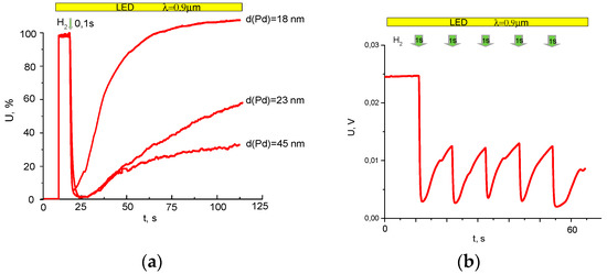
The Pd layer thickness of MOS structures was varied from 18 to 45 nm in different experiments. As can be seen from Figure 2a, the thinerPd layer thickness the faster the photovoltage recovery time.

Figure 2.
(a) Kinetics of photovoltage changing under the hydrogen exposure at LED (λ = 0.9 μm) illumination for the diodes with different Pd layer thicknesses; (b) Kinetics of the photovoltage under series of hydrogen pulses.
After the series of the short hydrogen pulses we observed the cycle decrease of photovoltage and its return to the initial level Figure 2b.
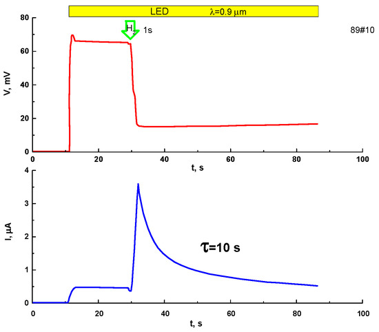
In Figure 3, one can see the kinetic changes of the photovoltage and the photocurrent in the presence of hydrogen.

Figure 3.
Kinetic changes in the photovoltage Voc and the photocurrent Isc under the exposure of hydrogen and LED illumination (λ = 0.9 μm, current of 10 mA) on the Pd/anodic oxide/InP structure. Sample 89#10, the oxide-layer thickness δ = 1000 Å, where τ, s is photocurrent-decay time constant.
After switching on the LED (λ ≈ 0.9 μm), the photovoltage appears within fractions of second and remains almost constant before the inlet of hydrogen. After the pulsed effect of hydrogen with a duration of 1 s, we observed a sharp drop of the photovoltage and, then, its slow return to the initial level begins.
On the contrary, the photocurrent sharply increases after the hydrogen pulsed supply. Then the photocurrent decreases to the initial level with a time constant of ~10 s.
The variation mechanism of the photovoltage and photocurrent is considered. The decrease of the value of the photovoltage is attributed, in our opinion, to the fact that, upon illumination, the dissociation of hydrogen molecules into atoms sharply increases; then the atoms are ionized with the formation of electrons and protons. It is assumed that released electrons decrease work function of Pd that in turn leads to the barrier height lowering, and the photocurrent increases due to the thermionic emission of nonequilibrium electrons from the Pd layer into the semiconductor.
4. Conclusions
A new sensor element creation technology has been presented. The photodiodes based on the Pd/anodic oxide/InP structure have been fabricated and its physical and photoelectric properties under the exposure of hydrogen have been investigated. It was observed that there is a sharp decrease of the photovoltage with the pulse exposure of hydrogen. The photocurrent, on the contrary, is rapidly increased by the pulse of hydrogen. It was obtained that the thiner Pd layer thickness the faster the photovoltage recovery time. The response signal time from 0.1 to 0.9 of maximal value of the signal was about 1 s.
Conflicts of Interest
The founding sponsors had no role in the design of the study; in the collection, analyses, or interpretation of data; in the writing of the manuscript, and in the decision to publish the results.
References
- Aroutiounian, V.M. Hydrogen Detectors. Int. Sci. J. Altern. Energy Ecol. 2005, 3, 21–30. [Google Scholar]
- Hübert, T.; Boon-Brett, L.; Black, G.; Banach, U. Hydrogen sensors—A review. Sens. Actuators B 2011, 157, 329–352. [Google Scholar] [CrossRef]
- Podlepetsky, B.; Nikiforova, M.; Kovalenko, A. Chip Temperature Influence on Characteristics of MISFET Hydrogen Sensors. In Proceedings of the Procedia Engineering of the 30th Eurosensors Conference, Budapesht, Hungary, 4–7 September 2016; Volume 168, pp. 251–254. Available online: www.sciencedirect.com (accessed on 8 August 2017).
- Pohle, R.; Weisbroda, E.; Hedler, H. Enhancement of MEMS-Based Ga2O3 Gas Sensors by Surface Modifications. In Proceedings of the Procedia Engineering of the 30th Eurosensors Conference, Budapesht, Hungary, 4–7 September 2016; Volume 168, pp. 211–215. Available online: www.sciencedirect.com (accessed on 8 August 2017).
- Chen, H.-I.; Chou, Y.-I.; Chu, C.-I. A Novel High-Sensitive Pd/InP Hydrogen Sensor Fabricated by Electroless Plating. Sens. Actuators B 2002, 85, 10–18. Available online: www.elsevier.com/locate/sensorb (accessed on 8 August 2017). [CrossRef]
- Kovalevskaya, G.G.; Kratena, L.; Meredov, M.M.; Marinova, A.M.; Slobodchikov, S.V. Photodetector Pd-interfacial layer-InP as the hydrogen sensor. Technol. Phys. Lett. 1989, 15, 55–58. [Google Scholar]
- Grebenshchikova, E.A.; Evstropov, V.V.; I’inskaya, N.D.I.; Mel’nikov, Y.S.; Serebrennikova, O.Y.; Sidorov, V.G.; Sherstnev, V.V.; Yakovlev, Y.P. Electrical Properties of Pd-Oxide-InP Structures. Semiconductors 2015, 49, 364–366. [Google Scholar] [CrossRef]
- Imenkov, A.N.; Grebenshchikova, E.A.; Shutaev, V.A.; Yakovlev, Y.P. Photovoltage and photocurrent in Pd-oxide-InP structures in a hydrogen medium. Semiconductors 2016, 50, 929–934. [Google Scholar] [CrossRef]
Publisher’s Note: MDPI stays neutral with regard to jurisdictional claims in published maps and institutional affiliations. |
© 2017 by the authors. Licensee MDPI, Basel, Switzerland. This article is an open access article distributed under the terms and conditions of the Creative Commons Attribution (CC BY) license (https://creativecommons.org/licenses/by/4.0/).