Abstract
Systems with high-temperature superconductors (HTSC) impose new requirements on power conversions, since the main part of the losses in such systems is induced in the semiconductors of the converters. Within the framework of this study, the possibility of improving the static and dynamic characteristics of power semiconductor diodes using cryogenic cooling was confirmed; in some cases, a loss reduction of up to 30% was achieved.
1. Introduction
To improve the weight and size parameters of generation and electric propulsion systems, electric machines and cable lines based on high-temperature superconducting materials of the second generation (HTSC-2) can be used [1]. In such systems, it is impossible to consider an electric machine in isolation from other elements, especially electronic converters. At present, in the vast majority of cases, an electric machine works in conjunction with a semiconductor energy converter: a power factor corrector, a rectifier, an electric motor controller, etc. These devices, which are directly connected to the windings of the electrical machine, affect the harmonic composition of the phase currents. The harmonic composition of the current is a very important parameter for HTSC windings since the losses in them strongly depend on it [2]. Studies conducted at the Department 310 MAI have shown that when a non-linear load is supplied from a generator with HTSC windings, an active correction of the shape of the phase currents using a power electronic converter is necessary. Otherwise, the losses from the higher current harmonics can be so great that the cryosupport system can no longer cope with heat removal and the super-conductor will go into a normal state.
Due to the fact that superconducting electrical machines require the presence of a cryogenic cooling circuit, it seems appropriate to investigate the possibility of integrating power semiconductor converters into this circuit. Cooling the heatsinks of power semiconductor devices with liquid nitrogen can also have a positive effect on the weight and size parameters of the system. It is proposed to use indirect cryogenic cooling of converters by pumping liquid nitrogen through tubes built into the radiator (the so-called cold plate). In this regard, it must be emphasized that the temperature of semiconductor components can fluctuate over a wide range with this method of cooling [3]. It also means that the lowest achievable temperature of the component will be higher than the boiling point of liquid nitrogen.
The main problem of the development of cryogenic cooling of power semiconductors is the unexplored effect of cryogenic cooling of components on the operation of the device. Since temperature and thermal processes are the main factor determining reliability, this issue is a priority. In particular, this follows from the various expansion coefficients of materials that can not only destroy the internal structure of the component, but also completely destroy the printed circuit board of the device [4].
There are a fairly large number of studies devoted to determining the characteristics of electronic semiconductor components at the boiling point of liquid nitrogen [5,6,7,8]. However, there are very few works in which power semiconductor devices are tested in the entire temperature range from +25 °C to −195.75 °C. Among them, we can highlight as the most outstanding, for example, [9], some works where the diode model of promising structures was corrected with experimental confirmation; and [10], where the static and dynamic characteristics of semiconductors were considered in a wide temperature range. However, the information presented in these publications is not universal, since the behavior of the characteristics of each particular semiconductor component is unique. This article is devoted to the experimental determination of the static characteristics of some power semiconductor diodes in a given temperature range and the analysis of the obtained dependencies.
2. Materials and Methods
To determine the dependence of the characteristics of power semiconductor devices on temperature in the range from −195.75 °C to +25 °C, a special test bench was developed and manufactured.
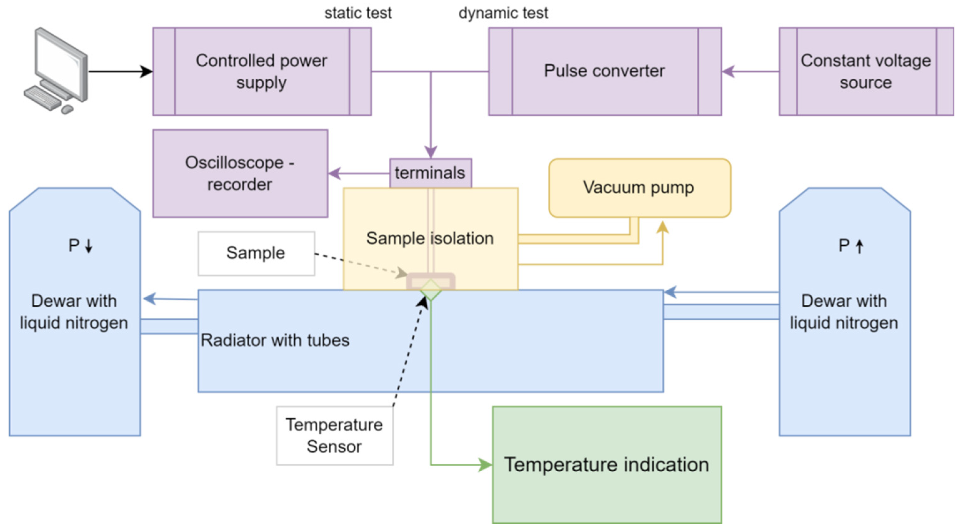
The device under study is mounted on a radiator through the tubes from which liquid nitrogen is pumped. The temperature sensor is attached to the heatsink as close as possible to the component under test. To control the temperature, the flow of liquid nitrogen is controlled using a manual valve. To prevent the formation of frost on the surface of the component under study, the space surrounding the component is evacuated.
When the valve is opened, the flow of liquid nitrogen under the action of pressure injected in the first Dewar vessel is pushed out through the tube towards the radiator. For a sufficiently long time, nitrogen passes through the tubes in a gaseous state. Once the radiator is cool enough, nitrogen begins to flow through the tubes in a liquid state and drains into a second open Dewar vessel. Cooling occurred at a rate of approximately 2–5 K per minute, which made it possible to measure the static and dynamic parameters of the diodes at a certain temperature, set with an accuracy of one degree. Measurements were made in steps of 10 K from 293 K to the minimum achievable temperature, which was 100 K with this method of cooling. The block diagram of the test bench is shown in Figure 1.

Figure 1.
Structural diagram of the test bench.
As part of the tests for temperature measurement, an OVEN 2TRM1 thermostat was used as an indicator and a DTS324-100P.VZ.41/0.5 sensor compatible with it. The absolute error of temperature measurement is the sum of the error of the temperature controller and the temperature sensor, and in total is 3.35–3.5 K. The appearance of the test bench is shown in Figure 2.
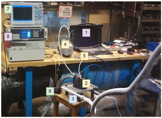
Figure 2.
Photo of the test bench. 1—computer that controls the source of test signals, 2—vacuum casing, 3—radiator with tubes, 4—vacuum pump, 5—pressure sensor, 6—temperature indicator, 7—oscilloscope recorder, and 8—source of test signals.
For static tests, a Kepco BOP 10–100 MG controlled current source was used. The signal was controlled using PC with NI SignalExpress 2014 and NI SCB-68a. During dynamic tests, two TEC 14 power supplies connected to a pulsed transistor power amplifier were used to form a bipolar signal. As a result of static tests, a current–voltage characteristic (CVC) was obtained.
A Yokogawa DL850E oscilloscope–recorder was used as a means of measuring electrical parameters and recording data. In the study of static characteristics, a Yokogawa 720,250 measuring module was used to record the parameters, and a Yokogawa 720,211 measuring module was used for dynamic characteristics. Both modules make it possible to measure voltage with an error of 0.5% of the maximum value of the selected range [11]. The stand measurement errors are presented in Table 1.

Table 1.
Characteristics of the measured signals.
The current values during static tests were calculated based on the voltage values on the measuring shunt made using low-inductance resistors LVR03, with an accuracy of 1%. The sensor contains 10 LVR03 resistors connected in parallel and has a resistance of 0.001 ohm.
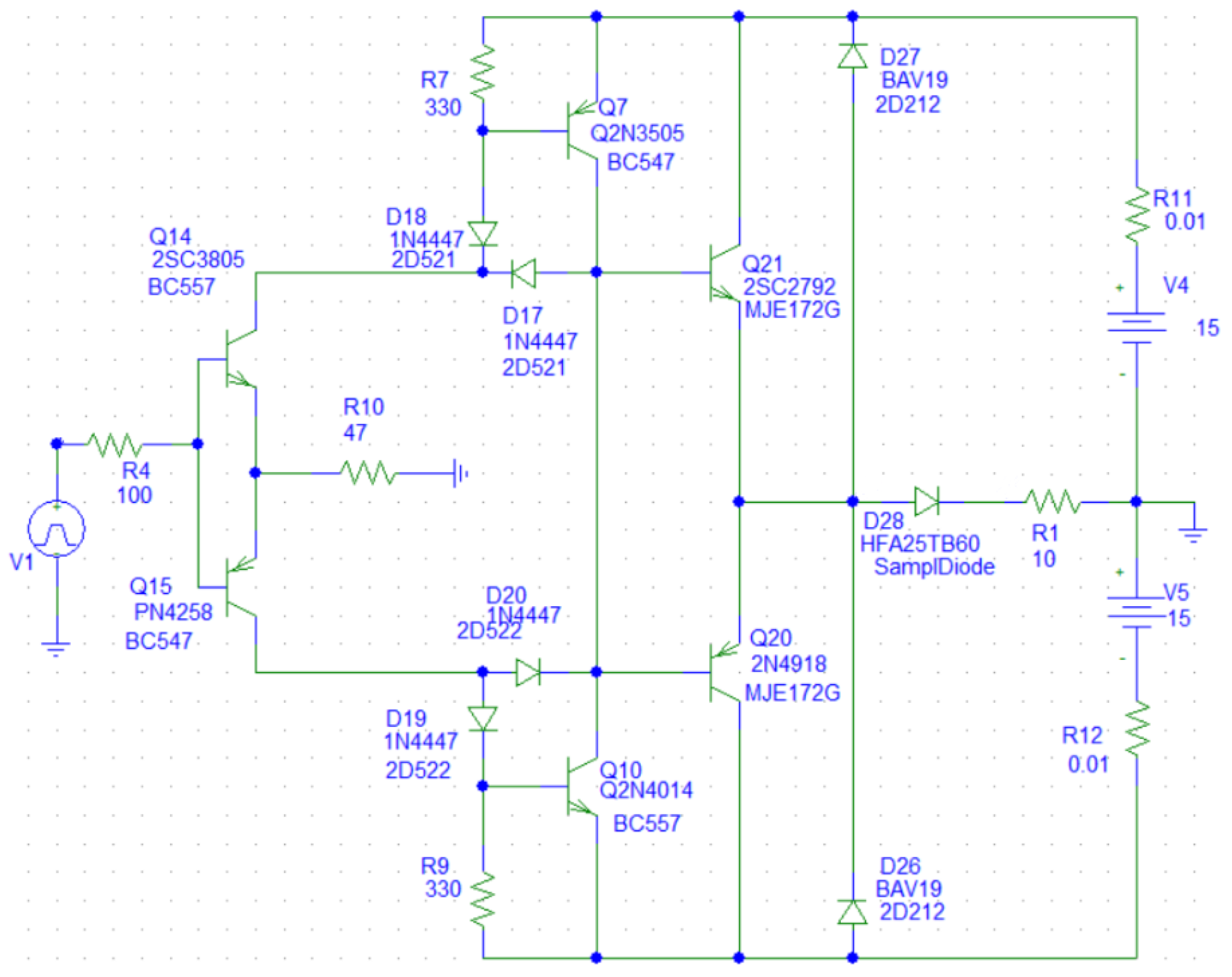
To study the dynamic characteristics of a diode, a test signal of a special shape is required. This is due to the high rate of reverse recovery processes of modern diodes. In the case of a test signal with a low switching rate, the reverse recovery processes may be hardly noticeable, or even absent. To form the corresponding signals, a pulsed transistor power amplifier was developed, the simulation computer model of which is shown in Figure 3.
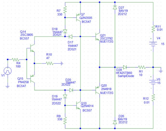
Figure 3.
Simulation model of a pulsed amplifier in the OrCad program.
The amplifier is assembled using high-frequency complementary bipolar transistors. To prevent the saturation of transistors, non-linear Baker circuits on diodes D17–D20 are used. The amplifier is controlled using the Aktakom signal generator, which in Figure 4 is represented by a source of pulsed voltage V1. The signal generator ensures the rise and fall time of the pulse is no more than 20 ns.

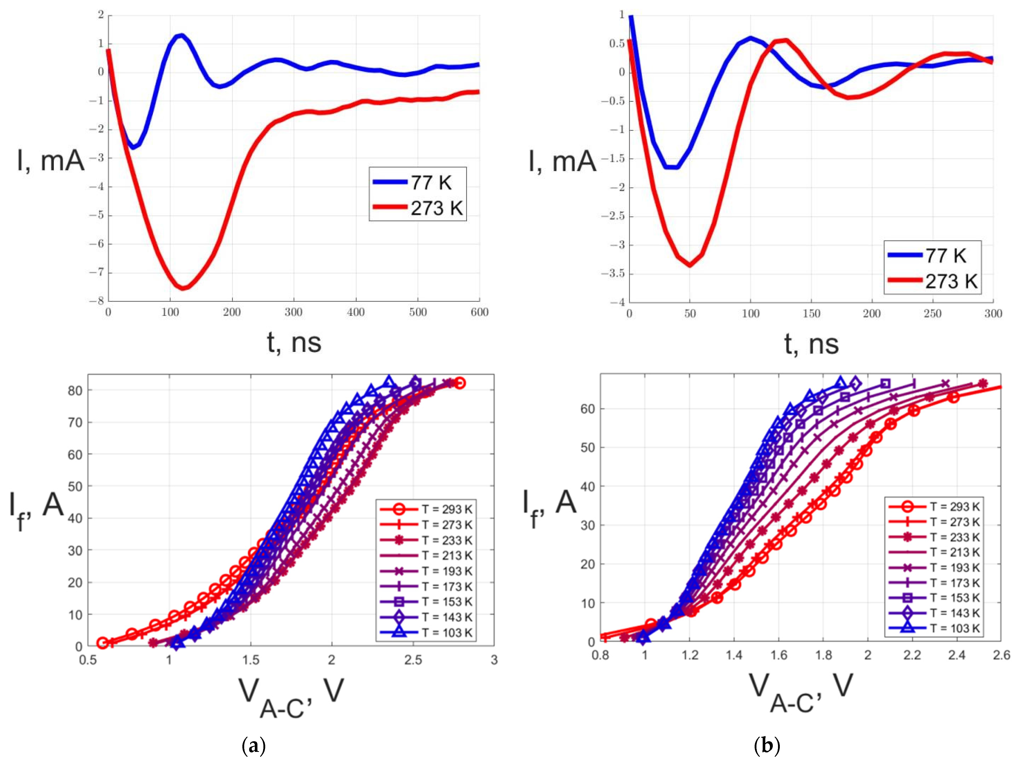
Figure 4.
Graphs of the reverse recovery process (top) of the samples and the forward branch of the CVC (bottom) for samples 1 (a) and 2 (b).
A problem with both static and dynamic testing is the heating of the semiconductor component crystal by the test signal. This means that during the test pulse, as the current increases, the temperature difference between the sensor and the crystal also increases. This causes an additional error in estimating the temperature of the component. This error can be estimated using either analytical calculations (assuming that the heating process is adiabatic) or finite element analysis. In both cases, it is necessary to be aware of the design of the semiconductor device and its thermophysical properties, including the heat capacities of all the structural elements. Obtaining this information is a very difficult task. In this regard, in this work, the temperature of the radiator of the studied component was measured de facto. In addition, it should be noted that the test signal is a small series of short pulses with low energy, which allows us to assume that the temperature of the crystal of the device under study will slightly differ from the temperature of the radiator.
For processing and outputting graphs in the .wdf format, the Mathworks MatLab program version 2022a with the WDF Access add-on was used.
3. Results
During the tests, the dynamic and static characteristics of power silicon diodes were obtained. The components used by the authors in current developments were selected as samples. The list of components is presented in Table 2.

Table 2.
Characteristics of the studied samples.
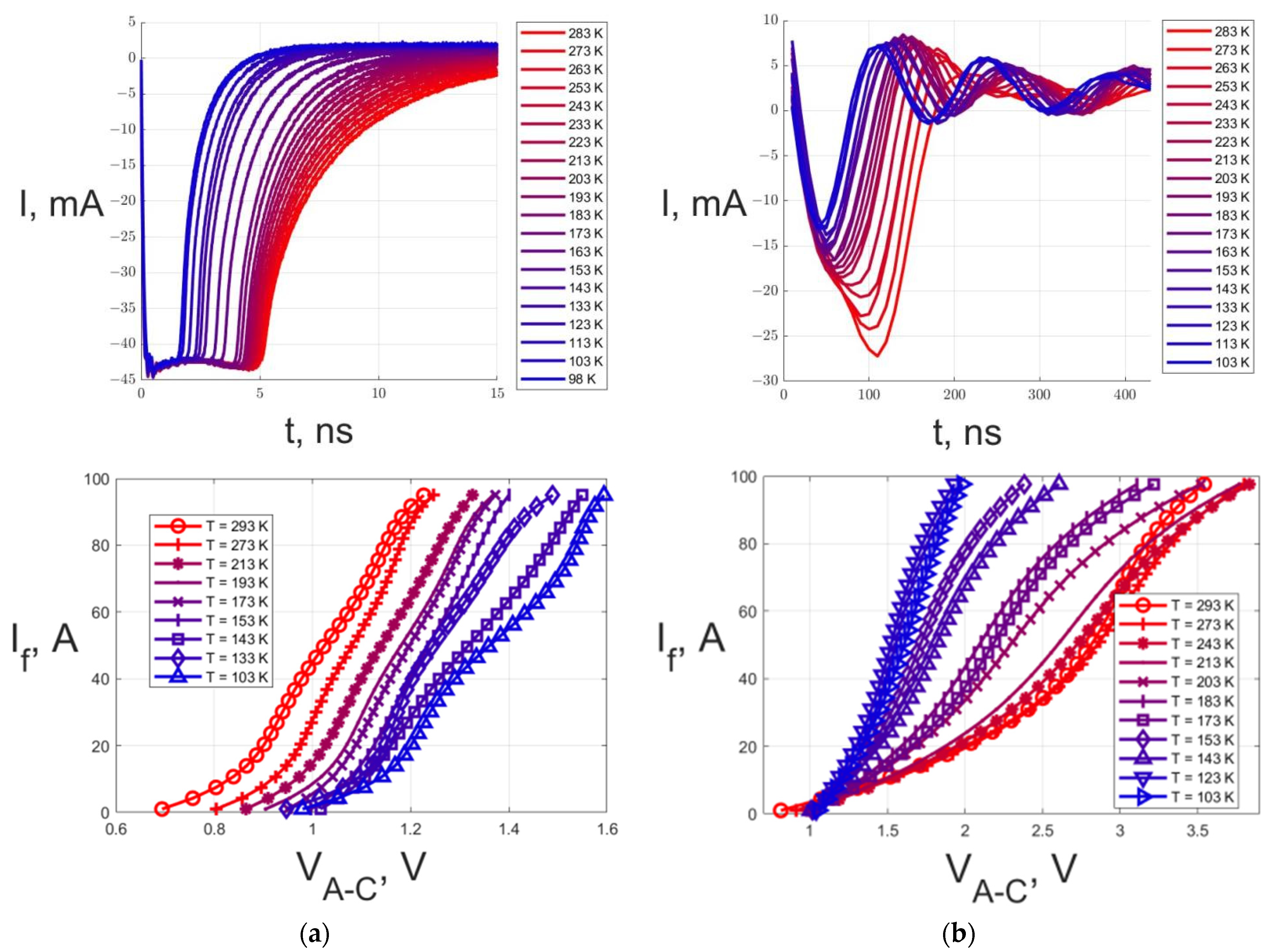
Figure 4 and Figure 5 show the graphs of the reverse recovery process obtained as a result of experiments and the direct branch of the CVC. For samples 1 and 2, due to some circumstances, the dynamic characteristics were investigated only for two temperatures.
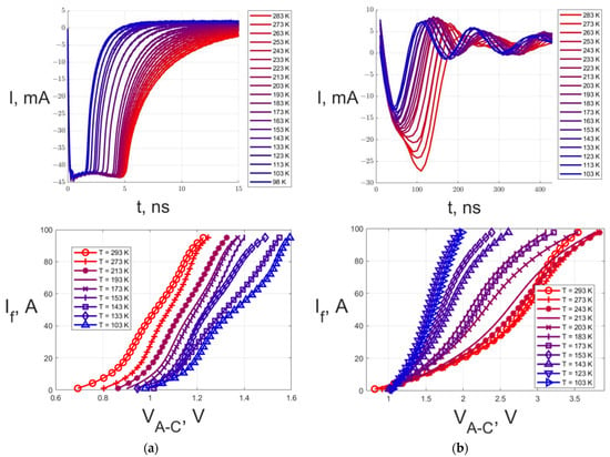
Figure 5.
Graphs of the reverse recovery process (top) of the samples and the forward branch of the CVC (bottom) for samples 3 (a) and 4 (b).
The dynamic characteristics showed a uniform change in the form of a decrease in dynamic losses. This is also associated with a decrease in the reverse recovery time of the diode. If we pay attention only to the characteristics of sample 4 (Figure 5a), then we can assume that the reverse recovery time decreases almost linearly with decreasing temperature. However, the nature of the change in the reverse recovery process of sample 3 suggests that, in fact, there is a reduction in the reverse recovery stage with the most intense current strength (Figure 5b). This is confirmed by the non-linearity of the transition point from the amplitude value of the reverse recovery current to the value of the leakage current.
In addition, it should be noted that the recovery process of samples 1, 2, and 4 has an oscillatory character. This may be due to the influence of the parasitic inductance of the design and capacitance of the pn junction of the diode at low reverse recovery times (samples 1,2, and 4 belong to the class of “fast” diodes).
The change in static characteristics with temperature is less unambiguous. The threshold voltage of the diodes in all cases increased with decreasing temperature. This can be seen from the transfer of the minimum current at a lower temperature in the direction of increasing voltage for each diode.
It is important to note a significant indicator of the change in static losses—the voltage drop across the diode for a given forward current. Since the region of high currents was chosen, then the studied components will reveal three options for changing this indicator. In the first case, there was an increase in voltage with decreasing temperature; in the second—a decrease; and in the third—a non-linear nature of the changes. The non-linear nature of the changes in the voltage drop at a given current was revealed in sample 1, which at first showed a tendency to increase the voltage in the region of high currents with a decrease in temperature, and after a certain temperature, the reverse process began. The CVC of sample 3 can be attributed to the first type, and samples 2 and 4, to the second. The CVC of samples 2 and 4 suggest a significant energy benefit from the use of cryogenic cooling in the case of prevailing static losses during the normal operation of the converter.
4. Discussion
To obtain an estimate of the change in static losses according to the CVC, the dependencies shown in Figure 6 were built. They reflect the ratio of the power of static losses at different temperatures to the maximum heat release, which for different devices falls at different temperatures. Thus, the resulting set of such energy characteristics is approximately in the same range and a numerical assessment of the change in static losses for each characteristic is possible. Given the equal sampling frequency of the oscilloscope, the losses were calculated as the average instantaneous power at positive currents and voltages of the test signal.
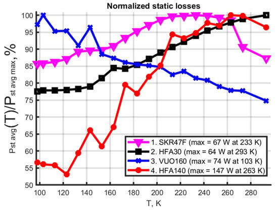
Figure 6.
Normalized static losses.
Based on the characteristics obtained, it can be concluded that the voltage drop at a given forward current has a strong influence on the resulting static losses. A decrease in this indicator corresponds to a decrease in static losses. The following conclusion can be made on the fact that it is energetically more profitable to use diodes in the region of higher currents in cryogenic cooling.
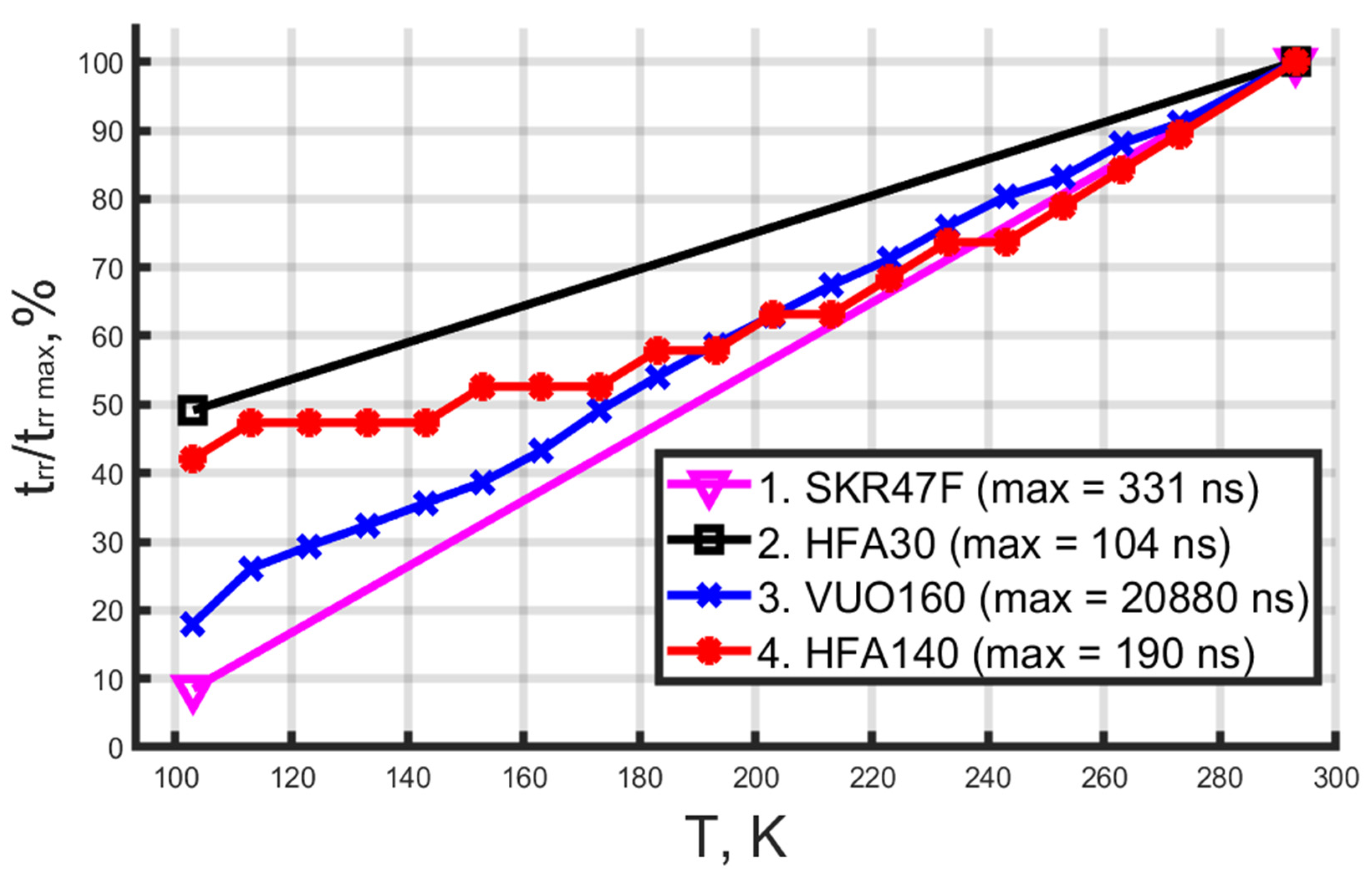
The dynamic loss during diode reverse recovery is calculated as the average of the power dissipated. The decrease in dynamic losses is explained by a decrease in the charge that is accumulated by the diode in the off state as the temperature decreases. This leads to both a decrease in the reverse recovery time and a decrease in the amplitude of the reverse recovery current in the case of samples 2–4. Characteristics normalized by the maximum value are shown in Figure 7 and Figure 8. In contrast to static losses, the maximum losses in the reverse recovery process are recorded at a maximum temperature of 293 K. This point corresponds to the maximum reverse recovery time for all the samples.

Figure 7.
Dependencies of the normalized values of the reverse recovery time on temperature.
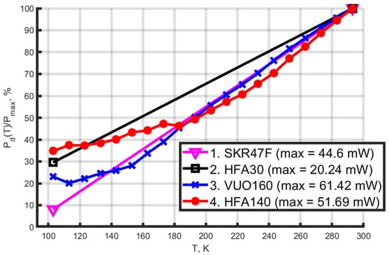
Figure 8.
Dependencies of the normalized losses in the process of reverse recovery on temperature.
Dynamic losses are an indicator that depends on the actual mode of operation of the diode. In the case of a single reverse recovery process, this only suggests an idea of how the dynamic losses will change, not allowing you to accurately calculate how the dynamic losses will change during the normal operation of the proposed device. However, this indicator allows one to obtain an estimate of heat dissipation using oscillographic measurements in a real circuit.
If it is advisable to cool electronics with liquid nitrogen, this will improve the efficiency of all devices where liquid nitrogen cooling is already used (for example, in MRI). In addition, this effect can be used with other refrigerants used as fuel—liquefied natural gas or liquid hydrogen.
5. Conclusions
In the course of studying the influence of low and cryogenic temperatures on the static and dynamic characteristics of power silicon semiconductor diodes, the dependencies of the current–voltage characteristics and the reverse recovery time on temperature were obtained for several samples in the range from +25 °C to −195.75 °C.
Based on the results of the study, it can be concluded that further research is promising in the field of using cryogenic cooling of power stages of semiconductor converters operating in the same system with superconducting electrical machines. This conclusion is based on the fact that both static and dynamic parameters of power semiconductor diodes demonstrate such a tendency with decreasing crystal temperature, which should lead to a decrease in both types of losses.
In order to confirm the rationality of such a solution, further studies of the effect of cryogenic temperatures on the static and dynamic characteristics of power semiconductor components, including power transistors, are required. The final conclusion can be made only after testing a real power semiconductor converter with experimental determination of losses in its elements.
Separately, it should be emphasized that for the practical application of cryogenic cooling in power electronics, it is necessary to study the effect of thermal cycling on the electrical parameters of semiconductor components and their design. This may be the subject of further research.
Author Contributions
Conceptualization, D.S. (Daniil Shevtsov) and D.S. (Dmitry Shishov); methodology, D.S. (Dmitry Shishov); software, M.O.; validation, S.Z., D.S. (Daniil Shevtsov), and D.S. (Dmitry Shishov); formal analysis, M.O.; investigation, M.O.; resources, D.S. (Dmitry Shishov); data curation, S.Z.; writing—original draft preparation, M.O.; writing—review and editing, D.S. (Dmitry Shishov) and S.Z.; visualization, M.O.; supervision, D.S. (Daniil Shevtsov); project administration, D.S. (Dmitry Shishov); funding acquisition, D.S. (Dmitry Shishov). All authors have read and agreed to the published version of the manuscript.
Funding
The study was carried out with the financial support of a project by the Russian Federation represented by the Ministry of Education and Science of the Russian Federation, agreement No. 075- 15-2020-770.
Institutional Review Board Statement
Not applicable.
Informed Consent Statement
Not applicable.
Data Availability Statement
Not applicable.
Conflicts of Interest
The authors declare no conflict of interest.
References
- Kovalev, K.L.; Ivanov, N.S.; Penkin, V.T.; Development of HTSC electrical machines and devices at MAI. Status and prospects for the development of electrical and thermal technology (Benardos readings). In Proceedings of the Materials International (XX All-Russian) Scientific and Technical Conference, Ivanovo, Russia, 29–31 May 2019; Ivanovo State Power Engineering University named after V.I. Lenin: Ivanovo, Russia, 2019; pp. 153–156. [Google Scholar]
- Zanegin, S.Y.; Ivanov, N.S.; Shishov, D.M.; Shishov, I.M.; Kovalev, K.L.; Zubko, V.V. AC losses test of HTS racetrack coils for HTS motor winding. J. Phys. Conf. Ser. 2020, 1559, 012142. [Google Scholar] [CrossRef]
- Wang, F.; Chen, R.; Gui, H.; Niu, J.; Tolbert, L.; Costinett, D.; Blalock, B.; Liu, S.; Hull, J.; Williams, J.; et al. MW-Class Cryogenically-Cooled Inverter for Electric-Aircraft Applications. In Proceedings of the 2019 AIAA/IEEE Electric Aircraft Technologies Symposium (EATS), Indianapolis, IN, USA, 22–24 August 2019; pp. 1–9. [Google Scholar] [CrossRef]
- Korobkov, M.; Vasilyev, F.; Mozharov, V. A Comparative Analysis of Printed Circuit Boards with Surface-Mounted and Embedded Components under Natural and Forced Convection. Micromachines 2022, 17, 634. [Google Scholar] [CrossRef] [PubMed]
- Elwakeel, A.; Feng, Z.; McNeill, N.; Zhang, M.; Williams, B.; Yuan, W. Study of power devices for use in phase-leg at cryogenic temperature. IEEE Trans. Appl. Supercond. 2021, 31, 1–5. [Google Scholar] [CrossRef]
- Pereira, P.; Valtchev, S.; Pina, J.; Gonçalves, A.; Neves, M.V.; Rodrigues, A.L. Power electronics performance in cryogenic environment: Evaluation for use in HTS power devices. J. Phys. Conf. Ser. 2008, 1, 012219. [Google Scholar] [CrossRef]
- Chen, S.; Cai, C.; Wang, T.; Guo, Q.; Sheng, K. Cryogenic and high temperature performance of 4H-SiC power MOSFETs. In Proceedings of the 2013 Twenty-Eighth Annual IEEE Applied Power Electronics Conference and Exp osition (APEC), Long Beach, CA, USA, 17–21 March 2013; pp. 207–210. [Google Scholar] [CrossRef]
- Singh, R.; Baliga, B.J. Cryogenic operation of PiN power rectifiers. Solid-State Electron. 1994, 37, 1833–1839. [Google Scholar] [CrossRef]
- Chen, J.; Zhu, M.; Lu, X.; Zou, X. Electrical characterization of GaN Schottky barrier diode at cryogenic temperatures. Appl. Phys. Lett. 2020, 116, 062102. [Google Scholar] [CrossRef]
- Wei, Y.; Hossain, M.M.; Mantooth, H.A. Static and Dynamic Cryogenic Characterizations of Commercial High Performance GaN HEMTs for More Electric Aircraft. In Proceedings of the 2022 International Power Electronics Conference (IPEC-Himeji 2022-ECCE Asia), Himeji, Japan, 15–19 May 2022; pp. 2300–2306. [Google Scholar]
- YOKOGAWA TEST & MEASUREMENT CORPORATION. Plug-in Modules Specifications; ScopeCorder Series DL950/DL850E/DL850EV/DL350/SL1000; 2021 Printed in Japan. Available online: https://cdn.tmi.yokogawa.com/1/8934/files/BUDL950-02EN.pdf (accessed on 13 July 2022).
Publisher’s Note: MDPI stays neutral with regard to jurisdictional claims in published maps and institutional affiliations. |
© 2022 by the authors. Licensee MDPI, Basel, Switzerland. This article is an open access article distributed under the terms and conditions of the Creative Commons Attribution (CC BY) license (https://creativecommons.org/licenses/by/4.0/).

