Abstract
In this work, two advanced technologies were applied for manufacturing a bimorph wavefront corrector: laser ablation, to vaporize conductive silver coating from piezoceramic surface, and parallel-gap resistance microwelding, to provide a reliable electrical contact between the piezodisk surface silver electrodes and copper wires. A step-by-step guide for bimorph mirror production is presented, together with the ‘bottlenecks’. Optimization of the laser ablation technique was carried out using an Nd:YAG laser with an output power of 4 W and a frequency of 20 kHz. A comparison of the ultrasonic welding and parallel-gap resistance microwelding methods was performed. The tensile strength in the first case was in the range of 0.2…0.25 N for the system ‘copper wire–silver coating’. The use of resistance welding made it possible to increase the value of this parameter for the same contact pair by almost two times (0.45…0.5 N).
1. Introduction
The evolution of adaptive optics is associated with the problem of developing reliable and miniature devices for the compensation of laser beam aberrations [1,2,3]. Wavefront correctors are an essential part of any adaptive optical system [4,5,6]. The main function of this element as an executive unit is to directly compensate distortions in light radiation through changes in shape by means of various mechanisms: electrostatic [7], pneumatic [8], electromagnetic [9], or piezoelectric [10,11]. Different types of correcting devices have been proposed and developed [12,13,14,15,16]. Moreover, there is a tendency to produce such devices with high numbers of control elements [17] and increased wavefront corrector reliability [18], while simultaneously reducing the final product price. The most suitable types of deformable mirror, due to their low cost and high reliability, are bimorph ones [19,20]. Moreover, our scientific group is widely known for the development of such wavefront correctors [21,22,23,24,25]. Nevertheless, there is a problem in the creation of these flexible mirrors resulting from the high spatial resolution of the control electrodes.
High-tech methods and materials are widely used for manufacturing bimorph wavefront correctors. For example, the CVD technique for the production of mirror substrates with embedded cooling channels [26] and additive technologies like laser stereolithography have been applied [27,28]. Moreover, nanotechnological methods such as magnetron sputter deposition and evaporation for the creation of reflective or conductive coatings for adaptive mirrors are widespread [29,30].
Small-aperture bimorph mirrors should be produced using innovative methods such as ultrasonic welding [31], parallel-gap contact microwelding [32], and laser ablation [33] techniques.
In the second section of this article, the key principle and the design of the bimorph deformable mirror are demonstrated, along with the main manufacturing steps. The third section presents a description of production technologies that make it possible to reduce the corrector size (mirror diameter) and to provide the stable performance of the adaptive optical element. In Section 4, the results of manufacturing a bimorph deformable mirror with a small aperture and a high density of control elements are presented.
2. Materials and Methods
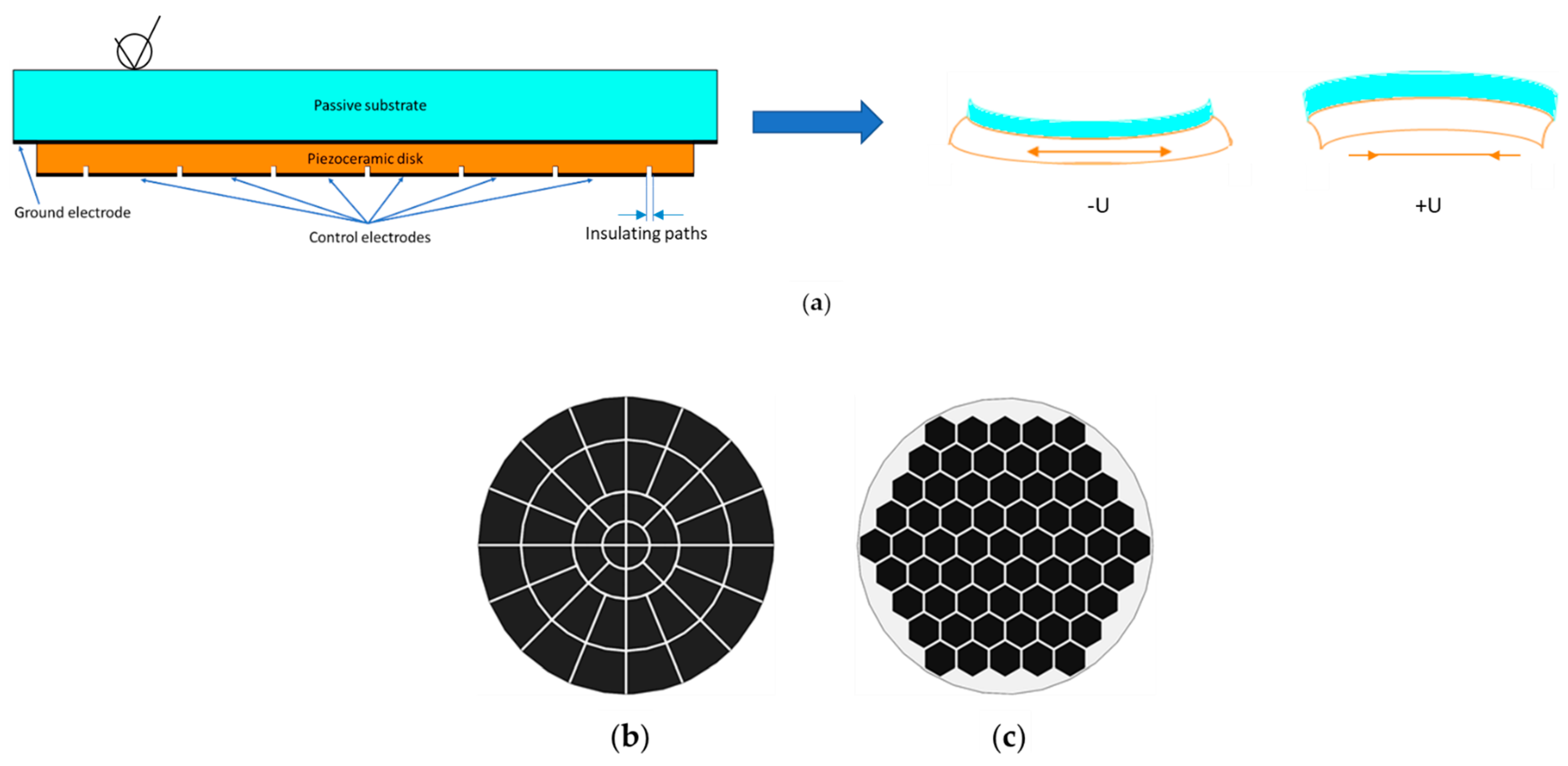
Bimorph flexible mirrors consist of a polished passive substrate made of glass, silicon or copper, along with an active piezoceramic plate with the conductive layer of silver or nickel (Figure 1a). On the outer surface of the piezoplate, an electrode grid is placed (Figure 1b,c). While applying control voltages to the electrodes, the transverse piezoceramic effect leads to the expansion (or compression) of the piezoplate, causing deformation (bend) to the mirror surface. By varying the control signals on the electrodes, the desired shape of the reflective surface can be realized.
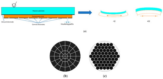
Figure 1.
Traditional bimorph deformable mirror: (a) conventional design and principle of operation, (b) keystone electrode grid, (c) honeycomb electrode grid.
The main steps of manufacturing traditional bimorph mirrors are as follows: (1) the piezoceramic plate is glued to the passive substrate; (2) after that, the electrode grid is drawn on the piezo plate surface using the photolithographic technique; (3) the substrate is polished in order to obtain a high-quality reflecting (mirror) surface; (4) in the next step, a highly reflective coating is deposited (>99.9%); (5) by using conductive glue, the contact wires are connected to the mirror electrodes; and finally, (6) the electrical wiring and mirror assembly are placed in the housing.
This manufacturing process for bimorph correctors is necessary for mirrors with average (30–100 mm) and large (>100 mm) apertures. Furthermore, during assembly, preliminary mechanical correction is performed for large-aperture mirrors by changing the tension of the adjustment screws located in the mounting. This technical solution makes it possible to reduce the influence of the initial aberrations (astigmatism, coma) arising from assembly and deposition of the reflective coating [34].
However, in the case of probing of the atmosphere using LiDAR [35], in free space communication systems [36] or in laser materials processing [37], as well as in microscopy [38], it is necessary to use small-aperture mirrors (<30 mm). At the same time, the number of control elements should be sufficient to compensate for both low- and high-order wavefront aberrations [39]. The deformable mirror should also provide a reasonable stroke of the reflective surface in order to compensate for large-scale wavefront aberrations. Increasing the local deflection of the mirror can be achieved by using a thin passive substrate, but its thickness must be sufficient to avoid the print-through effect of the control electrode grid [40].
Piezoceramic is a porous material, which leads to some inconveniences with respect to placing the electrode grid on its surface. The traditional technique of chemically etching the insulating paths in the conductive layers deposited on the piezodisk is not quite applicable in this case. Nevertheless, this process has proven to be an ideal tool for the creation of dielectric paths in bimorph deformable mirrors, and can be applied for average- and large-aperture mirrors [41]. Therefore, to avoid short circuit between neighbor electrodes, it is necessary to make rather wide paths. The particles of the conductive material (silver or nickel) might penetrate inside the ceramic hollows, thus creating unnecessary electrical connection between electrodes. At the same time, different methods for creating insulating paths (dielectric tracks) on the disk surface using laser the ablation technique can lead to the unexpected removal of piezoceramic material. This might destroy the whole piezodisk, and as a result introduce the so-called print-through effect on the mirror surface [30].
Additionally, the wiring of the electric contacts is an important problem arising during the manufacturing of small-aperture deformable mirrors because of the reduced size of both the electrodes and the contact area (to 5–12 mm2). For such an electrode size, the traditional gluing methods with the conductive epoxy are not suitable. The use of conventional soldering methods is impossible as well, considering that the heating of the piezodisk will result in the local depolarization of the piezoceramic, resulting in the failure of the mirror.
For this reason, to overcome these problems, we propose the use of laser ablation and microwelding techniques for the development of bimorph wavefront correctors.
Laser ablation methods are widely used for the synthesis of colloidal nanoparticles in liquids [42] and nanostructural coatings [43]. Additionally, this technique can be applied for the removal of layers from various surfaces of materials [44]. The working principle is as follows: the light from the emitter passes through a set of mirrors to the objective lens and is focused on the object surface. During the processing, the upper layers of the treated material evaporate, and after that, insulating paths between electrodes appear. For the treatment of different metals, lasers with the wavelength of about 1 μm are applied [45], such as Nd:YAG-lasers. Additionally, lasers with a second-harmonic generation mode can often be used.
We exploited a laser ablation setup with a Q-switched Nd:YAG laser with a pulse energy of 0.67 mJ, a pulse duration of 100 ns, and a frequency repetition rate in the range from 20 to 200 kHz. Average laser radiation power was up to 20 W. The minimal focal spot on the object surface was about 50 μm. Laser ablation technology possesses the favorable characteristics of high processing speed and precise materials treatment. Additionally, the full automatization of the process guarantees the high repeatability of the results unlike the chemical etching. Nevertheless, the use of such a technique is restricted by the non-uniformity of the layers of the workpieces [46]. As was mentioned earlier, the overheating of the bimorph plate can result in additional initial distortions of the reflective surface of the mirror and decrease the efficiency of correction of wavefront aberrations. Obviously, depending on the piezoplate properties (conductive layer thickness, material of coating), the parameters of the laser beam for electrode coating removal should be adjusted.
In our case, we used piezoceramic disks with a thickness of 0.2 mm. Their surface was coated with a conductive silver layer with a thickness of about 20 μm. In the setup for creating insulating paths, a radiation with an average power of 4 W with a pulse frequency of 20 kHz was used. The width of the dielectric tracks was chosen as 300 μm to avoid electrical breakdown between electrodes during mirror operation.
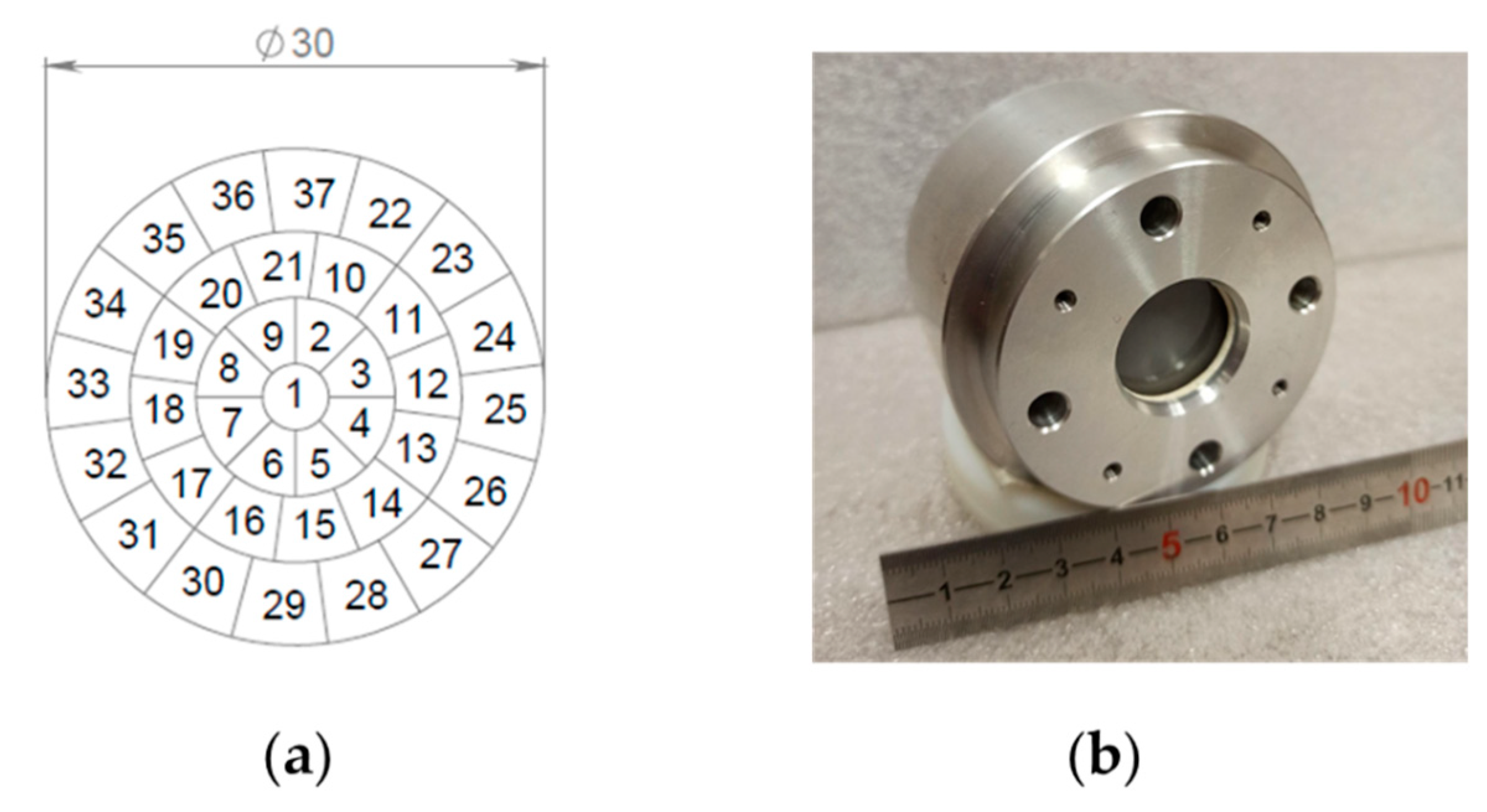
Using these ablation parameters, we manufactured a piezoplate with 37 electrodes in a keystone geometry on a 30 mm aperture (Figure 2). Thus, the average area of one electrode was equal to 10 mm2. An alternative method to gluing techniques for wiring electrical contacts for this bonding area, in our opinion, is microwelding approaches (thermocompression, ultrasonic, parallel-gap resistance microwelding), which are widely used in contemporary microelectronics.
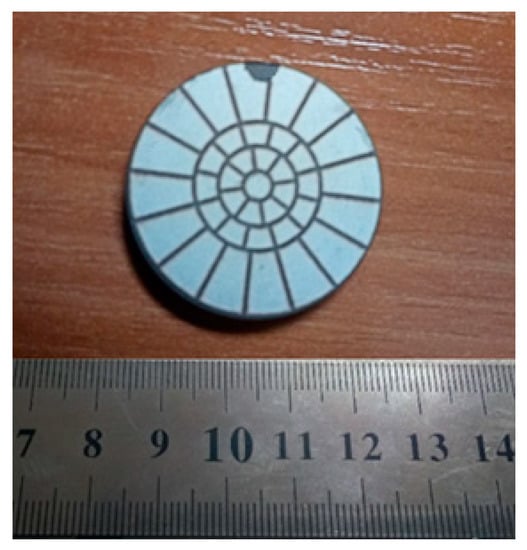
Figure 2.
The electrode grid placed on the piezodisk surface.
Pad-to-pad wiring is one of the most widely used approaches for bonding electrotechnical elements [47]. Traditional welding methods are almost never used, because of the small sizes of the contact areas. Microcontacts are realized, as a rule, by means of gold, aluminum, or copper 30–150 μm wires. In our work, we chose three widely used microwelding methods—thermocompression, ultrasonic, parallel-gap resistance. We analyzed the most suitable welding techniques for the design of bimorph deformable mirrors.
Thermocompression welding is used to attach the pins to the semiconductor crystals, for welding the microwires, for welding the flat cable cores to connector pins, etc. [48]. However, the local heating of the processing materials can result in temperatures of up to 650 °C. Such high thermal stresses can damage the structure of the welding components, meaning that this technique cannot be used for the manufacture of piezoelectric deformable mirrors.
To overcome this disadvantage the ultrasonic approach of microcontacting was proposed. This method is characterized by the application of ultrasonic energy to the contact area [49]. This results in bursting and burning of the solid fatty films in the region of the connection point, the plastic deformation of the material and intensive diffusion. The high-frequency vibrations lead to a reliable connection of the workpieces by means of the plastic deformations of the welding parts. We carried out experiments in which aluminum and copper wires (with the diameter of 50…100 μm) were welded to various surfaces (Al, Cu, Ag).
However, it should be mentioned that, together with the minimal heating stresses, we were not able to achieve a significant value for tensile strength P. For the contact system ‘aluminum wire (diameter d = 80 μm)–silver film (thickness h = 20 μm)’ the tensile strength value with ultrasonic microwelding was PAl(US) = 0.15…0.20 N, and for the system ‘copper wire (d = 80 μm)–silver film (h = 20 μm)’ the tensile strength value increased to PCu(US) = 0.2…0.25 N.
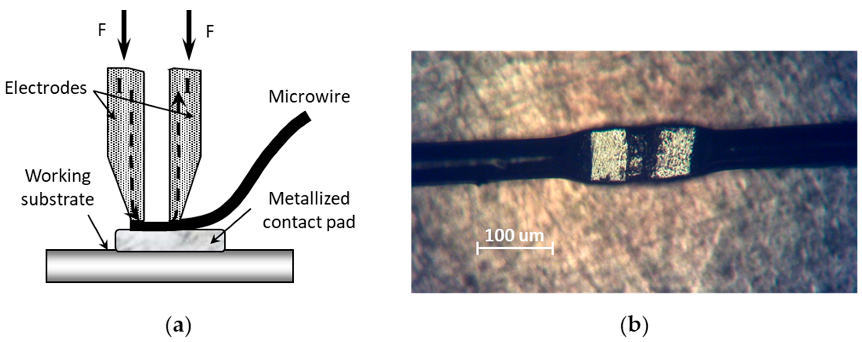
Greater values of PCu were obtained when using the parallel-gap microwelding technique. This approach is a variation of the resistance welding method [32] adapted for the design features of deformable piezoelectric mirrors (Figure 3a). The welding materials in this case were copper, aluminum and silver. The thickness of the silver films was in the range of 15–25 μm, and the diameter of the copper and aluminum wires was 80 μm. Tungsten was used as an electrode material.

Figure 3.
Parallel-gap resistance microwelding: (a) scheme of setup, (b) result of welding of copper wire to silver coating on piezodisk.
Before welding, the workpieces were annealed to decrease their inner stresses and increase their plasticity. The surfaces of the materials were also degreased with chemical solvents. The welding process was performed with an electrode made of tungsten as the current-conductive parts, with a gap of 0.02…0.25 mm depending on the thickness and diameter of the workpieces.
The efficiency of parallel-gap resistance microwelding was estimated by analysis of the ensile strength value. For contact pair ‘copper wire (d = 80 μm)–silver film (h = 20 μm)’, this parameter was PCu(R) = 0.45…0.50 N, depending on the various welding regimes.
In Figure 3b, the results of welding copper wire with a diameter of 80 μm to silver film with a thickness of 20 μm on the piezoceramic plate as part of the bimorph deformable mirror are shown.
3. Results and Discussion
The optimization of the traditional laser ablation and parallel-gap resistance microwelding techniques for adaptive optics tasks made it possible to manufacture a 37-electrode bimorph deformable mirror (Figure 4a,b) with an active diameter of 30 mm.
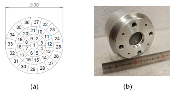
Figure 4.
Developed bimorph deformable mirror: (a) electrode grid, (b) assembled deformable mirror.
After assembling the bimorph deformable mirror, we investigated its main parameters—the initial quality of the reflective surface (as the most important characteristic), local and total stroke of the mirror, and the first resonant frequency.
The initial surface quality was measured using a Fizeau interferometer Zygo Mark GPI-XPS. As seen in Figure 5a, the print-through effect was not visible on the reflective surface of the mirror. The initial surface distortions were equal to PV = 1.72 μm, RMS = 0.46 μm, when taking into account the total surface curvature (Figure 5b), and PV = 0.42 μm, RMS = 0.08 μm without defocus aberration (Figure 5c). The presence of astigmatism aberration is intrinsic to the initial surface because of the fixing mechanism of the bimorph wavefront corrector in the housing.
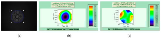
Figure 5.
Initial shape of the developed deformable mirror: (a) image as interferogram, (b) initial surface quality with the total curvature (PV = 1.72 μm, RMS = 0.46 μm), (c) initial surface without defocus aberration (PV = 0.42 μm, RMS = 0.08 μm).
To measure the stroke of the mirror, we used a diagnostic setup based on a Shack-Hartmann wavefront sensor, simulating the conventional closed-loop adaptive optical system (Figure 6). The setup consisted of a diode laser with an average output power of 5 mW at a wavelength of 650 nm, a lens with a focal length of 500 mm, the bimorph deformable mirror, and a Shack–Hartmann wavefront sensor [50]. The wavefront sensor included a CMOS camera, a lenslet with the microlens focal length of 5 mm and a pitch of 120 μm, and a 6× beam-reducing telescope. To adjust the optical system, a tracer laser with a narrow parallel beam with a wavelength of 650 nm was used. The radiation of this laser was propagated through the centers of the optical elements. The diagnostic and tracer laser beams were combined on the diaphragm.
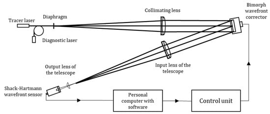
Figure 6.
Diagnostic setup for investigation of the parameters of the deformable mirror.
It is obvious that the local stroke of the inner electrodes will be smaller than that of electrodes at the periphery of the mirror. Therefore, we measured the value of this parameter for two different electrodes—#7 and #32. The stroke was found to be 1.4 μm (PV) and 4.7 μm (PV) for the 7th and 32nd electrodes, respectively. These values are comparable to those of bimorph deformable mirrors with significantly larger electrode areas [51].
Additionally, we measured the total stroke of the developed deformable mirror. We applied the maximum control voltage to all mirror electrodes in order to achieve formation of defocus aberration. The largest value was equal to 12 μm (PV).
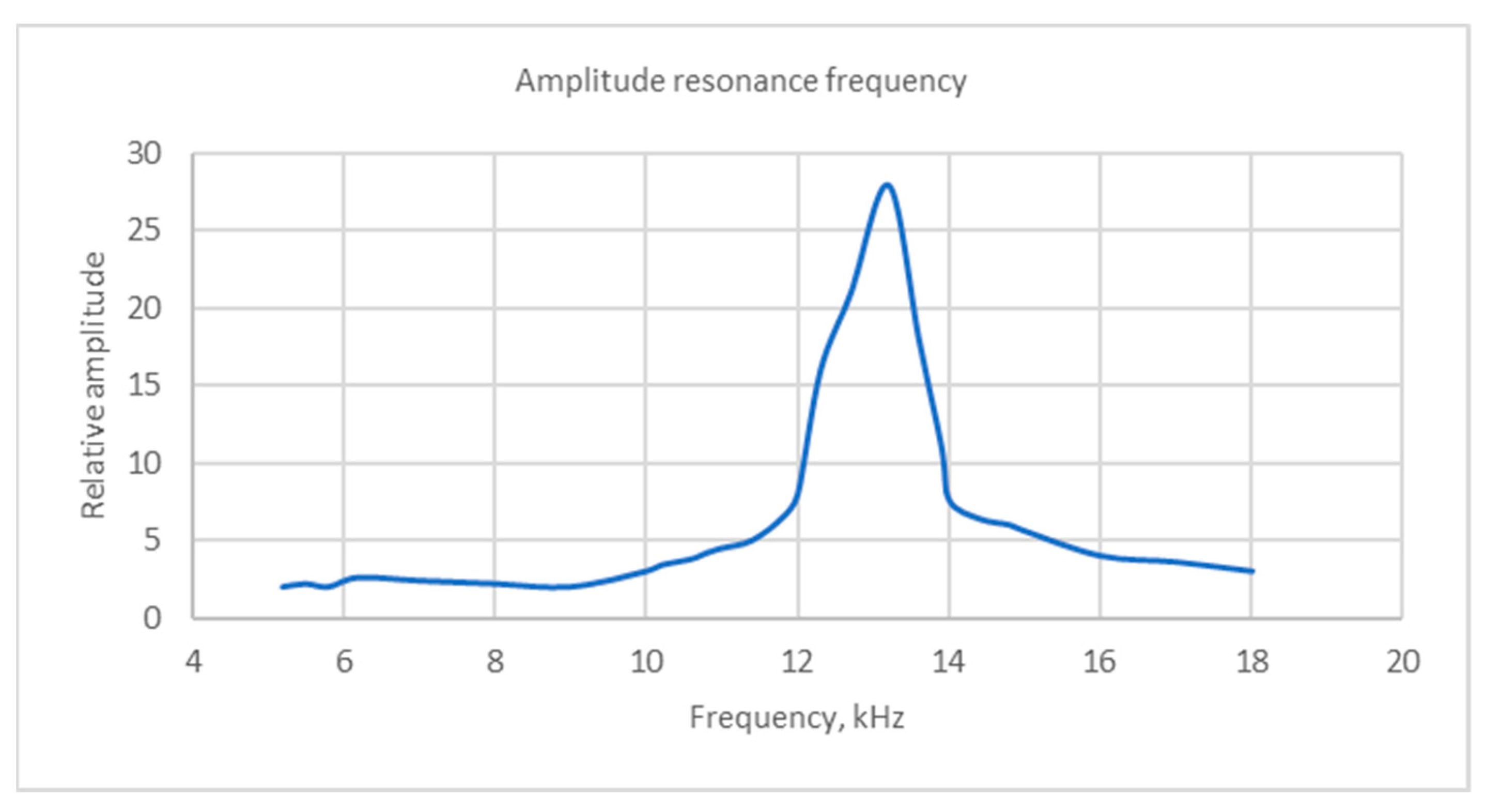
One of the significant parameters in deformable mirror operation in closed-loop adaptive optical systems is speed—how fast the mirror can introduce different wavefront aberrations. This parameter is directly related to the first resonant frequency of the wavefront corrector. For bimorph mirrors, it can be estimated using the following formula [52]:
where K—scaling coefficient depending on the boundary conditions (shown in Table 1) [53], D—effective elastic constant for the plate, g—gravitational acceleration, w—loading per unit area of the plate, including its own weight (, and tk correspond to the density and thickness of each layer).

Table 1.
Values of the scaling constant K for different boundary conditions.
Thus, the estimated value of the first resonant frequency for the bimorph mirror with an overall thickness of 1.6 mm (0.2 mm for piezoceramic and 1.4 mm for glass substrate) should be equal to 13.4 kHz. To measure the real value of this parameter, we used an oscilloscope Tektronix DPO-2004B and a sine wave generator. A sine voltage with a frequency range from 0.1 to 18 kHz was applied to electrode #1. Due to the piezoelectric effect, AC voltage was detected on the neighboring electrode #2 and was registered using the oscilloscope [54]. The amplitude of the output signal was stable up to a frequency of 12 kHz, and the first resonance was found at a frequency of 13.2 kHz (Figure 7). More detailed analysis of the temporal behavior using the Bode curve [55] shows the possibility of using such a deformable mirror in a closed-loop adaptive system working with a frequency (in terms of frames per second) of 10 kHz.

Figure 7.
Amplitude–frequency response of the bimorph wavefront corrector.
4. Conclusions
We developed a 37-electrode bimorph deformable mirror with a diameter of 30 mm. The results of using the laser ablation technique were demonstrated. This technique was proposed for removing the silver coating from the piezodisk surface. Using the Q-switched Nd:YAG laser with an average power of 4 W and a repetition rate of 20 kHz made it possible to obtain insulating paths with a width of 300 μm. It was shown that by using the ultrasonic welding approach for bonding the copper wires to the silver contact pad of the piezodisk, it was possible to achieve a tensile strength value in the range of PCu(US) 0.2…0.25 N, while the parallel-gap resistance microwelding technique made it possible to increase this value by two times (PCu(R) = 0.45…0.5 N). The stroke of the single electrode of the mirror varied from 1.4 μm to 4.7 μm, depending on electrode position. The maximum total stroke of the bimorph corrector was equal to 12 μm. The first resonant frequency of the mirror was found at 13.2 kHz. Such a deformable mirror would be useful for the compensation of low-order and high-order aberrations caused by atmospheric turbulence.
Author Contributions
Conceptualization, A.K. and A.S.; methodology, A.S.; software, I.G.; validation, V.T., V.S. and A.R.; formal analysis, V.T. and V.S.; investigation, V.T. and A.R.; resources, A.K.; data curation, V.T. and V.S.; writing—original draft preparation, V.T. and A.K.; writing—review and editing, V.T. and A.K.; visualization, V.T. and I.G.; supervision, V.S.; project administration, A.K.; funding acquisition, A.K. All authors have read and agreed to the published version of the manuscript.
Funding
The investigations of the mirror manufacturing methods (Chapter 2) were supported by the Russian Science Foundation under grant #19-19-00706P, and the investigation of the mirror properties (Chapter 3) was supported by the state assignment of the Ministry of Science and Higher Education of the Russian Federation (theme No122032900183-1).
Institutional Review Board Statement
Not applicable.
Informed Consent Statement
Not applicable.
Data Availability Statement
The data that supports the findings of this study are available from the corresponding author upon reasonable request.
Conflicts of Interest
The authors declare no conflict of interest.
References
- Bendek, E.; Lynch, D.; Pluzhnik, E.; Belikov, R.; Klamm, B.; Hyde, E.; Mumm, K. Development of a miniaturized deformable mirror controller. Proc. SPIE 2016, 9909, 990984. [Google Scholar] [CrossRef] [Green Version]
- Divoux, C.; Cugat, O.; Basrour, S.; Mounaix, P.; Kern, P.Y.; Boussey-Said, J. Miniaturized deformable magnetic mirror for adaptive optics. Proc. SPIE 1998, 3353, 850–857. [Google Scholar] [CrossRef]
- Toporovsky, V.; Kudryashov, A.; Samarkin, V.; Panich, A.; Sokallo, A.; Malykhin, A.; Skrylev, A.; Sheldakova, J.V. Small-aperture stacked-array deformable mirror made of the piezoceramic combs. Proc. SPIE 2021, 11672, 1167215. [Google Scholar] [CrossRef]
- Sato, T.; Ishida, H.; Ikeda, O. Adaptive PVDF piezoelectric deformable mirror system. Appl. Opt. 1980, 19, 1430–1434. [Google Scholar] [CrossRef]
- Wei, K.; Zhang, X.; Xian, H.; Ma, W.; Zhang, A.; Zhou, L.; Guan, C.; Li, M.; Chen, D.; Chen, S.; et al. First light on the 127-element adaptive optical system for 1.8-m telescope. Chin. Opt. Lett. 2010, 8, 1019–1021. [Google Scholar] [CrossRef]
- Kudryashov, A.; Rukosuev, A.; Nikitin, A.; Galaktionov, I.; Sheldakova, J. Real-time 1.5 kHz adaptive optical system to correct for atmospheric turbulence. Opt. Express 2020, 28, 37546–37552. [Google Scholar] [CrossRef]
- Bifano, T. MEMS deformable mirrors. Nat. Photonics 2021, 5, 21–23. [Google Scholar] [CrossRef]
- Moghimi, M.J.; Wilson, C.; Dickensheets, D.L. Electrostatic-pneumatic MEMS deformable mirror for focus control. In Proceedings of the 2012 International Conference on Optical MEMS and Nanophotonics, Banff, AB, Canada, 6–9 August 2012; pp. 132–133. [Google Scholar]
- Biasi, R.; Gallieni, D.; Salinari, P.; Riccardi, A.; Mantegazza, P. Contactless thin adaptive mirror technology: Past, present, and future. Proc. SPIE 2010, 7736, 77362B. [Google Scholar] [CrossRef]
- Toporovsky, V.V.; Kudryashov, A.V.; Samarkin, V.V.; Rukosuev, A.L.; Nikitin, A.N.; Sheldakova, Y.V.; Otrubyannikova, O.V. Cooled Stacked-Actuator Deformable Mirror for Compensation for Phase Fluctuations in a Turbulent Atmosphere. Atmospheric Ocean. Opt. 2020, 33, 584–590. [Google Scholar] [CrossRef]
- Samarkin, V.; Aleksandrov, A.G.; Jitsuno, T.; Romanov, P.N.; Rukosuev, A.L.; Kudryashov, A. Study of a wide-aperture combined deformable mirror for high-power pulsed phosphate glass lasers. Quantum Electron. 2015, 45, 1086–1087. [Google Scholar] [CrossRef]
- Lefaudeux, N.; Levecq, X.; Dovillaire, G.; Ballesta, J.; Lavergne, E.; Sauvageot, P.; Escolano, L. Development of a new tech-nology of deformable mirror for ultra-intense laser applications. Nucl. Instrum. Methods Phys. Res. Sect. A Accel. Spectrometers Detect. Assoc. Equip. 2011, 653, 164–167. [Google Scholar] [CrossRef]
- Salinari, P.; Del Vecchio, C.; Biliotti, V. A study of an adaptive secondary mirror. In Proceedings of the ICO-16 (International Commission for Optics) Satellite Conference on Active and adaptive optics, Garching/Munich, Germany, 2–5 August 1993; p. 247. [Google Scholar]
- Lück, H.; Müller, K.-O.; Aufmuth, P.; Danzmann, K. Correction of wavefront distortions by means of thermally adaptive optics. Opt. Commun. 2000, 175, 275–287. [Google Scholar] [CrossRef] [Green Version]
- Ivanova, N.L.; Onokhov, A.P.; Chaika, A.N.; Resnichenko, V.V.; Yeskov, D.N.; Gromadin, A.L.; Feoktistov, N.A.; Beresnev, L.A.; Pape, D.R. Liquid-crystal spatial light modulators for adaptive optics and image processing. Proc. SPIE 1996, 2754, 180–185. [Google Scholar] [CrossRef]
- Samarkin, V.V.; Alexandrov, A.; Toporovsky, V.; Rukosuev, A.; Kudryashov, A. Water-cooled deformable mirrors for high power beam correction. Proc. SPIE 2021, 11849, 1184917. [Google Scholar] [CrossRef]
- Riaud, P. New high-density deformable mirrors for high-contrast imaging. Astron. Astrophys. 2012, 545, A25. [Google Scholar] [CrossRef] [Green Version]
- Cornelissen, S.A.; Bifano, T.G.; Bierden, P.A. MEMS deformable mirror actuators with enhanced reliability. Proc. SPIE 2012, 8253, 47–53. [Google Scholar] [CrossRef]
- Oya, S.; Bouvier, A.; Guyon, O.; Watanabe, M.; Hayano, Y.; Takami, H.; Iye, M.; Hattori, M.; Saito, Y.; Itoh, M.; et al. Performance of the deformable mirror for Subaru LGSAO. Proc. SPIE 2006, 6272, 62724S. [Google Scholar]
- Alaluf, D.; Bastaits, R.; Wang, K.; Horodinca, M.; Martic, G.; Mokrani, B.; Preumont, A. Unimorph mirror for adaptive optics in space telescopes. Appl. Opt. 2018, 57, 3629–3638. [Google Scholar] [CrossRef]
- Kudryashov, A.V.; Kulakov, V.B.; Kotsuba, Y.V.; Novikova, L.V.; Panchenko, V.Y.; Samarkin, V.V. Low-cost adaptive optical devices for multipurpose applications. Proc. SPIE 1999, 3688, 469–476. [Google Scholar] [CrossRef]
- Galaktionov, I.; Sheldakova, J.; Nikitin, A.; Samarkin, V.; Parfenov, V.; Kudryashov, A. Laser beam focusing through a mod-erately scattering medium using a bimorph mirror. Opt. Express 2020, 28, 38061–38075. [Google Scholar] [CrossRef]
- Kudryashov, A.; Alexandrov, A.; Rukosuev, A.; Samarkin, V.; Galarneau, P.; Turbide, S.; Châteauneuf, F. Extremely high-power CO2 laser beam correction. Appl. Opt. 2015, 54, 4352–4358. [Google Scholar] [CrossRef] [PubMed]
- Wattellier, B.; Fuchs, J.; Zou, J.-P.; Chanteloup, J.C.; Bandulet, H.; Michel, P.; Labaune, C.; Depierreux, S.; Kudryashov, A.; Aleksandrov, A. Generation of a single hot spot by use of a deformable mirror and study of its propagation in an underdense plasma. J. Opt. Soc. Am. B 2003, 20, 1632–1642. [Google Scholar] [CrossRef]
- Samarkin, V.; Aleksandrov, A.; Dubikovsky, V.; Kudryashov, A. Water-cooled bimorph correctors. Proc. SPIE 2005, 6018, 60180Z. [Google Scholar] [CrossRef]
- Ahn, K.; Rhee, H.-G.; Yang, H.-S.; Kihm, H. CVD SiC deformable mirror with monolithic cooling channels. Opt. Express 2018, 26, 9724–9739. [Google Scholar] [CrossRef]
- Cholleti, E.R. A Review on 3D printing of piezoelectric materials. IOP Conf. Series Mater. Sci. Eng. 2018, 455, 012046. [Google Scholar] [CrossRef]
- Hall, S.E.; Regis, J.E.; Renteria, A.; Chavez, L.A.; Delfin, L.; Vargas, S.; Haberman, M.R.; Espalin, D.; Wicker, R.; Lin, Y. Paste extrusion 3D printing and characterization of lead zirconate titanate piezoelectric ceramics. Ceram. Int. 2021, 47, 22042–22048. [Google Scholar] [CrossRef]
- Hickey, G.; Barbee, T.; Ealey, M.; Redding, D. Actuated hybrid mirrors for space telescopes. Proc. SPIE 2010, 7731, 773120. [Google Scholar] [CrossRef]
- Rausch, P.; Verpoort, S.; Wittrock, U. Unimorph deformable mirror for space telescopes: Design and manufacturing. Opt. Express 2015, 23, 19469–19477. [Google Scholar] [CrossRef]
- Neppiras, E. Ultrasonic welding of metals. Ultrasonics 1965, 3, 128–135. [Google Scholar] [CrossRef]
- Biele, L.; Schaaf, P.; Schmid, F. Specific Electrical Contact Resistance of Copper in Resistance Welding. Phys. Status Solidi Appl. Mater. Sci. 2021, 218, 2100224. [Google Scholar] [CrossRef]
- Chichkov, B.N.; Momma, C.; Nolte, S.; Von Alvensleben, F.; Tünnermann, A. Femtosecond, picosecond and nanosecond laser ablation of solids. Appl. Phys. A 1996, 63, 109–115. [Google Scholar] [CrossRef]
- Samarkin, V.V.; Alexandrov, A.G.; Galaktionov, I.V.; Kudryashov, A.V.; Nikitin, A.N.; Rukosuev, A.L.; Toporovsky, V.V.; Sheldakova, Y.V. Large-aperture adaptive optical system for correcting wavefront distortions of a petawatt Ti: Sapphire laser beam. Quantum Electron. 2022, 52, 187–194. [Google Scholar] [CrossRef]
- Tan, X.-C.; Wu, Z.-C.; Liang, Z. Effect of adaptive optical system on the capability of lidar detection in atmosphere. Proc. SPIE 2009, 7284, 72840G. [Google Scholar] [CrossRef]
- Weyrauch, T.; Vorontsov, M. Free-space laser communications with adaptive optics: Atmospheric compensation experiments. J. Opt. Fiber Commun. Rep. 2004, 1, 355–379. [Google Scholar] [CrossRef]
- Spalding, I. Electric-discharge pumping. High Power Laser Sci. Eng. 1996, 7, 27. [Google Scholar]
- Booth, M.J. Adaptive optical microscopy: The ongoing quest for a perfect image. Light. Sci. Appl. 2014, 3, e165. [Google Scholar] [CrossRef]
- Noll, R.J. Zernike polynomials and atmospheric turbulence. J. Opt. Soc. Am. 1976, 66, 207–211. [Google Scholar] [CrossRef]
- Verpoort, S.; Rausch, P.; Wittrock, U. Characterization of a miniaturized unimorph deformable mirror for high power CW-solid state lasers. Proc. SPIE 2012, 8253, 825309. [Google Scholar] [CrossRef]
- Zhu, Z.; Li, Y.; Chen, J.; Ma, J.; Chu, J. Development of a unimorph deformable mirror with water cooling. Opt. Express 2017, 25, 29916. [Google Scholar] [CrossRef]
- Arakelyan, S.M.; Veiko, V.P.; Kutrovskaya, S.V.; Kucherik, A.O.; Osipov, A.V.; Vartanyan, T.A.; Itina, T.E. Reliable and well-controlled synthesis of noble metal nanoparticles by continuous wave laser ablation in different liquids for deposition of thin films with variable optical properties. J. Nanoparticle Res. 2016, 18, 155. [Google Scholar] [CrossRef]
- Takaku, R.; Wen, Q.; Cray, S.; Devlin, M.; Dicker, S.; Hanany, S.; Hasebe, T.; Iida, T.; Katayama, N.; Konishi, K.; et al. Large diameter millimeter-wave low-pass filter made of alumina with laser ablated anti-reflection coating. Opt. Express 2011, 29, 41745–41765. [Google Scholar] [CrossRef]
- Chryssolouris, G. Laser Machining-Theory and Practice; Springer: New York, NY, USA, 1991; 274p. [Google Scholar]
- Patel, R.; Chaudhary, P.S.; Soni, D.K. A review on laser engraving process for different materials. Int. J. Sci.-Entific Res. Dev. 2015, 2, 1–4. [Google Scholar]
- Toporovskii, V.V.; Skvortsov, A.A.; Kudryashov, A.V.; Samarkin, V.V.; Sheldakova, Y.V.; Pshonkin, D.E. Flexible bi-morphic mirror with high density of control electrodes for correcting wavefront aberrations. J. Opt. Technol. 2019, 86, 32–38. [Google Scholar] [CrossRef]
- Babu, S.; Santella, M.; Feng, Z.; Riemer, B.; Cohron, J. Empirical model of effects of pressure and temperature on electrical contact resistance of metals. Sci. Technol. Weld. Join. 2001, 6, 126–132. [Google Scholar] [CrossRef]
- Reinert, W. Handbook of Silicon Based MEMS Materials and Technologies. Met. Alloy. Seal Bond. 2015, 1, 626–639. [Google Scholar]
- Sprigode, T.; Gester, A.; Wagner, G.; Mäder, T.; Senf, B.; Drossel, W.-G. Mechanical and Microstructural Characterization of Ultrasonic Welded NiTiCu Shape Memory Alloy Wires to Silver-Coated Copper Ferrules. Metals 2021, 11, 1936. [Google Scholar] [CrossRef]
- Kudryashov, A.V.; Samarkin, V.V.; Sheldakova, Y.V.; Aleksandrov, A.G. Wavefront compensation method using a Shack-Hartmann sensor as an adaptive optical element system. Optoelectron. Instrum. Data Process. 2012, 48, 153–158. [Google Scholar] [CrossRef]
- Sheldakova, J.; Kudryashov, A.; Lylova, A.; Samarkin, V.; Byalko, A. New approach for laser beam formation by means of deformable mirrors. In Laser Beam Shaping XVI; SPIE: Bellingham, WA, USA, 2015; Volume 9581, p. 95810. [Google Scholar] [CrossRef]
- Young, W.C. Roark's Formulas for Stress and Strain, 6th ed.; McGraw-Hill: New York, NY, USA, 1989; pp. 421–442. [Google Scholar]
- Ellis, E.M. Low-Cost Bimorph Adaptive Mirrors. PhD Thesis, Imperial College of Science, London, UK, 1999. [Google Scholar]
- Toporovsky, V.; Samarkin, V.; Sheldakova, J.; Rukosuev, A.; Kudryashov, A. Water-cooled stacked-actuator flexible mirror for high-power laser beam correction. Opt. Laser Technol. 2021, 144, 107427. [Google Scholar] [CrossRef]
- Samarkin, V.; Alexandrov, A.; Galaktionov, I.; Kudryashov, A.; Nikitin, A.; Rukosuev, A.; Toporovsky, V.; Sheldakova, J. Wide-Aperture Bimorph Deformable Mirror for Beam Focusing in 4.2 PW Ti: Sa Laser. Appl. Sci. 2022, 12, 1144. [Google Scholar] [CrossRef]


Publisher’s Note: MDPI stays neutral with regard to jurisdictional claims in published maps and institutional affiliations. |
© 2022 by the authors. Licensee MDPI, Basel, Switzerland. This article is an open access article distributed under the terms and conditions of the Creative Commons Attribution (CC BY) license (https://creativecommons.org/licenses/by/4.0/).