Abstract
Electro-optic modulators in the near-infrared spectrum are finding applications in atomic clocks, quantum sensing, quantum information processing, and high-precision measurement. We developed thin-film lithium niobate electro-optic modulators operating at 795 nm for modulation around the D1 line of 87Rb with satisfactory overall performance. Specifically, we made a systematic improvement to reduce the insertion loss, including widening the modulation waveguides, thickening the overcladding, polishing and coating the facets. The fabricated device possesses a low insertion loss of 7.6 dB, an extinction ratio exceeding 30 dB, a 3 dB modulation bandwidth of ~22 GHz, a half-wave voltage-length product of ~1.8 Vcm, and strong adaptability for packaging.
1. Introduction
Electro-optic modulators (EOMs) function as the pivotal optical switch and valve in contemporary optoelectronic and information systems. They translocate electrical signals into the optical domain by exploiting electro-optic (EO) effects—such as the Pockels and Kerr phenomena—whereby an applied voltage or current directly perturbs the amplitude, phase, polarization, or frequency of light, thereby enabling real-time electro-optical transduction. Among the myriad EO materials, lithium niobate (LN) is a widely favored candidate. As a wholly synthetic material, the crystal structure of LN was first documented in 1928 [1]. Since the 1960s, when the properties of single-crystal LN were first systematically revealed [2,3,4,5,6,7], it has emerged as one of the most versatile and compelling optical materials in photonics, often hailed as the “silicon” of this field [8,9]. Due to its excellent linear EO effect, low intrinsic loss, and wide transparent wavelength window [10], it commands a substantial share of the global market of EOMs [11]. However, traditional bulk lithium niobate modulators face limitations because of the small refractive index difference resulting from titanium diffusion or photon exchange, which hinder achieving high EO efficiency; small device size; and high EO bandwidth [11]. Fortunately, the fabrication process of thin-film lithium niobate (TFLN) or, equivalently, LN on insulator (LNOI) has matured in the last two decades [12,13,14,15]. Thanks to this breakthrough, high-performance TFLN modulators are now becoming increasingly available.
EOMs operating in the near-visible (NV) spectrum play a crucial role in various scenarios, including atomic clocks, quantum computation and sensing, communication, and high-precision measurement [16,17,18,19]. However, traditional EO modulators are mainly in the telecom bands [15,20,21,22]. Less attention is given to the NV spectrum.
In recent years, photonics in the NV spectra has entered researchers’ view. Compared to its rivals such as Si or InP, which absorb NV light, TFLN has an overwhelming advantage due to its wide transparency window covering the whole visible and near-infrared spectra [22]. A Mach–Zehnder modulator (MZM) centered at 780 nm on lithium niobate on sapphire was demonstrated with a half-wave voltage-length product (VπL) of 1.26 Vcm and an EO bandwidth of 2.7 GHz [23]. The modulator occupies only 0.35 mm2 and allows dense wiring. A wide-spectrum visible EO modulator proposed in 2023 achieved a bandwidth of over 20 GHz, covering the entire visible spectrum from 400 to 700 nm [24]. A hybrid integrated MZM at 784 nm with TFLN bonded to planarized silicon nitride waveguides achieved a 3 dB EO bandwidth of 100 GHz and a VπL of 0.8 Vcm, demonstrating a record bandwidth-to-half-wave voltage (Vπ) ratio of 100 GHz/V [25].
However, the issue of insertion loss (IL) in NV wavelength modulation remains a significant concern that has yet to be adequately resolved. Rayleigh scattering loss, which scales proportionally to the inverse of the fourth power of the wavelength, significantly contributes to this challenge. Additionally, the optical field mode volume is smaller at shorter wavelengths, making it more difficult to couple light into the fiber. For instance, reference [26] notes that the coupling loss per facet of the modulator is as high as 10 dB, even though its VπL remains below 1 Vcm at frequencies up to 40 GHz. References [23,24] did not report the total loss. The lowest insertion loss reported to date is 12 dB, as mentioned in reference [25]. This achievement utilizes CMOS-compatible Si3N4 material for the peripheral circuit to enhance the coupling between the optical waveguide and the input/output fibers, albeit introducing added fabrication complexity due to heterogeneous bonding.
In this work, we demonstrate a NV thin-film lithium niobate EO modulator. Specifically, it operates at 795 nm, designed particularly for modulation around the D1 line of 87Rb. The modulator presents overall performance comparable to the state-of-the-art devices [27] while maintaining a simple fabrication process. We made significant efforts to reduce the IL. Drawing inspiration from the relevant methods used in silicon-based modulators, we achieved an IL of 7.6 dB by systematically addressing its multiple origins. This was accomplished by thickening the overcladding, widening the waveguides, and polishing and coating the waveguide ends, all through a thorough iteration of simulation and measurement. The device features an extinction ratio (ER) of approximately 31 dB, a 3 dB modulation bandwidth of 22 GHz, and a VπL of 1.8 Vcm, demonstrating robust adaptability for packaging.
2. Materials and Methods
The modulator operates on the basis of Mach–Zehnder interferometer structure built on LNOI. To conveniently leverage the largest EO coefficient of LN ( and avoid the complexity of backside electrodes deposition usually required by the z-cut scheme, we adopt the x-cut LN film to build our modulator [28,29]. Accordingly, the fundamental transverse electric (TE) mode, TE0 is modulated by microwaves along the c-axis of the LN crystal. A push–pull configuration doubles the voltage difference between the two arms and hence halves the half voltage-length product (VπL). Figure 1 shows the schematic of the TFLN modulator, including the top view and the cross-section view at the denoted position in the modulation region. Simple coplanar waveguide ground–signal–ground electrodes are employed to transmit radio-frequency (RF) signals. The parameters in Figure 1b are listed in Table 1. A layer of SiO2 is inserted between the electrodes and the waveguide to prevent metal absorption at their crossings. A thermo-optic phase shifter made of titanium is used to adjust the direct-current (DC) bias. The ground electrodes are widened such that the overall device width reaches ~3 mm to facilitate dicing between individual devices. All the pads are bent and extended to the device borders, perpendicular to the light coupling direction. This configuration also paves the way for packaging. The following subsections show detailed methods and design parameters of the design.
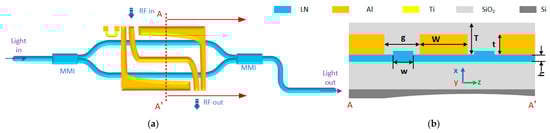
Figure 1.
Schematic of the modulation chip. (a) Planar view. (b) Sectional view. T represents the thickness of the overcladding. g is the gap between electrodes. W and t are the width and thickness of the signal electrode, respectively. h is the height of the LN slab. w is the width of the waveguide.

Table 1.
Key parameter values in our design.
2.1. Propagational Waveguide
Thick LN films operating at a short wavelength tend to accommodate transverse-magnetic (TM) modes as the fundamental mode. For instance, the fundamental mode is TM0 instead of the desired TE0 with a rib width from 300 nm to 700 nm in a 300 nm-high rib above a 300 nm slab at the wavelength of 795 nm, as illustrated in Figure 2a,b. Therefore, we employed a comparatively thin 300 nm X-cut TFLN platform (NanoLN, Jinan, China) to build our modulator. The rib height has a significant impact on both the VπL and metal absorption. Specifically, VπL increases monolithically with an increase in rib height. Meanwhile, the metal absorption increases as the rib gradually diminishes. Finally, an etching depth of 100 nm was determined. In this case, TE0 remains the fundamental mode when the waveguide width varies from 300 nm to 700 nm, as shown in Figure 2c,d.
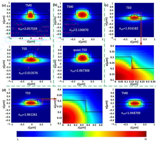
Figure 2.
Simulated optical eigenmode fields at 795 nm. (a) The first two modes of the highest effective indices in a 300 nm wide and 300 nm high rib on a 300 nm slab. (b) The first two modes of the highest effective indices in a 700 nm wide and 300 nm high rib on a 300 nm slab. The mode of the second highest effective index is of 99% TE polarization fraction which we denote as “quasi-TE0”. (c) The fundamental mode in a 300 nm wide and 100 nm high rib on a 200 nm slab. (d) The first two modes of the highest effective indices in a 700 nm wide and 100 nm high rib on a 200 nm slab. The black solid lines underpin the profiles of the waveguides. The enlarged views of the red-boxed areas illustrate the overlap degrees between the optical fields and the waveguides. All the effective indices are annotated in the backgrounds.
Single-TE0-mode waveguides are given by the Finite Difference Eigenmode method to be narrower than 300 nm. In such narrow waveguides, the volume of the optical mode is squeezed more into the slab downwards and then expands bilaterally as Figure 2c illustrates. Under these circumstances, Rayleigh scattering from the intersection areas of the slab and the rib deteriorates the transmission loss. Nonetheless, the TE0 mode remains the fundamental mode up to a waveguide width of 650 nm. Incorporating feedback from experiments, we design the “filter waveguides” to be 700 nm wide with the optical mode field distribution illustrated in Figure 2d. They are inserted before and after multimode interferometers (MMIs) to filter out higher TE modes exited in the preceding non-uniform areas while introducing minimum scattering loss.
2.2. Propagation in Beam Splitter
ER is an important metric for modulators. It is defined as the ratio of the power of the light in the “off” state to the power of the light in the “on” state, and is primarily determined by the splitting ratio of the beam splitter and combiner. MMIs are used as the splitter and the combiner to accommodate a relaxed fabrication tolerance. The schematic of the MMI is depicted in Figure 3. Tapers between the single-mode waveguides and the multimode waveguide mitigate their modal mismatch, thereby reducing additional losses [30]. The width of the filter, the intersection ports and the multimode waveguide are WS = 0.7 μm, Wt = 1.2 μm, WM = 8 μm, respectively. The length of the multimode waveguide and the adiabatic taper are LM = 92 μm, Lt = 50 μm, respectively. Simulated electromagnetic fields of the propagation and the output port are plotted in Figure 3b and Figure 3c, respectively, showing a clear splitting of light.
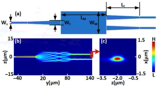
Figure 3.
Multimode interferometer. (a) Schematic diagram. (b) Propagation and interference pattern in the model. (c) The electric field distribution at the output port indicated by the red circle.
2.3. Modulation
Figure 4 illustrates the z-components of both the optical field and the modulation electric field, showing exactly the most effective components that lead to a modulation effect. The refractive index variation and can be deducted by [10]
and
where is the wavelength, is the driving voltage, is the extraordinary index of LN, is the EO coefficient at 795 nm, is the overlap between the optical and the electrical fields, is the gap between the electrodes, and is the modulation length. Given the inherently low at short wavelengths, an electrode gap of is adopted to prioritize reducing the metal absorption and relaxing the fabrication alignment requirement, despite the trade-off of a moderate increase in .
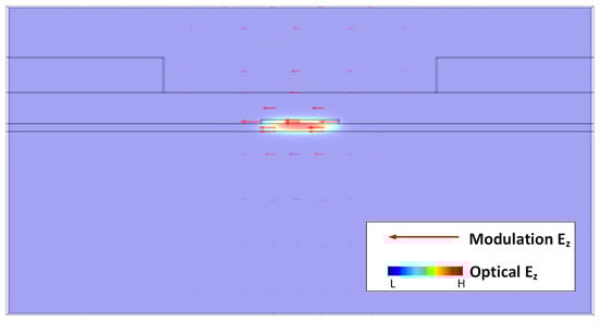
Figure 4.
Simulated electro-optic overlap. Red arrows indicate the direction and intensity of the z-component of the modulation electric field. Color map represents the intensity distribution of the z-component of the optical electric field.
2.4. Strategies on Reducing Insertion Losses
IL is a critical metric for the application of TFLN modulators, defined as the output power ratio with and without the modulator. It consists of the on-chip transmission loss and the input/output coupling loss, with the latter being the primary contributor. Rayleigh scattering from the intersections of the slab and the rib is the major contributor to propagation losses (refer to Figure 2 for visualization). To leverage the reduced sidewall-scattering losses in wider waveguides, we designed the modulation region’s waveguide width to be 2 μm. In the “filter” regions, which filter out higher-order modes originating from fiber coupling or waveguide non-uniformity, we tested modulators with waveguide widths of 600, 650, and 700 nm, all nearing the single-mode limit. Our measurements indicate a preference for the 700 nm filter waveguide. For access waveguides, we adopted single-layer tapers to achieve a more relaxed fabrication tolerance. The optimal width for the outmost section of the waveguide was determined through simulations to be 3.3 μm, ensuring the best coupling with the single-mode lensed fiber. To further reduce IL, we introduced an optical film as a buffer layer between the waveguide and the electrodes. This approach yields a smaller IL compared to the conventional plasma-enhanced chemical vapor deposition (PECVD), attributed to the optical film’s greater uniformity and smoothness.
Additionally, a thick silica layer is deposited on top to minimize the index disturbance caused by interface roughness. This facilitates a gentler and more gradual variation in refractive index, which reduces reflection losses at the interfaces. We tested the IL of a waveguide before and after regrowing the overcladding from 400 nm to 3400 nm, observing substantial variations. These changes may partly result from the challenges associated with aligning smaller facets; our adjustment mount’s precision is 1 μm, while the best sensitivity achievable through manual tuning is between 50 and 100 nm, often influenced by environment perturbations. Such unavoidable coupling deviations are likely to affect output optical power significantly.
The waveguide facets are post-processed by polishing and being coated with an anti-reflection (AR) film. A test conducted on a batch of fabricated modulators revealed that the polishing process can reduce IL by 0.5~3.5 dB, compared to the state before polishing. The AR film, consisting of a 136 nm silica layer, effectively mitigates Fresnel reflection, contributing an estimated IL reduction of about 0.6 dB per facet, which aligns well with the average measured data. Table 2 summarizes the reduction in IL achieved through various methods outlined above.
Table 2.
Reduction in IL by each method.
2.5. Fabrication
Figure 5 depicts the fabrication process. A 2 × 2 cm2 die of 300 nm thick X-cut TFLN on a 525 μm silicon substrate with a 4.7 μm SiO2 buffer layer in between was prepared via wafer dicing. Then, electron beam lithography (EBL) was used to pattern the waveguide with a resist AR-P 6200.09, which acted as the mask in the subsequent ion beam etching. SEM images were taken to examine the verticality, smoothness, straightness and width of the waveguides, as illustrated in Figure 6a–c, among which Figure 6a shows the cross-section of the modulation area, Figure 6b is the top view of a “filter” waveguide, and Figure 6c shows the MMI. Next, a layer of 800 nm thick SiO2 was deposited via optical deposition before the Ti resistor was fabricated via EBL, evaporation and lift-off. The Ti resistor had a length of 200 μm, a width of 3 μm and a thickness of 150 nm. It was close to the upper waveguide arm and was bent upwards to connect with the testing pads, as micrographed in Figure 6d. Thereafter, the electrode layer of Al was fabricated via photolithography, evaporation and lift-off. Figure 6e demonstrates the crossing area of the electrodes and the waveguides. Subsequently, another layer of SiO2 was deposited on the top via PECVD and the testing pads were revealed through reactive ion etching. Finally, polishing and coating at the waveguide facets were conducted, which are not depicted in the figure. Figure 6f shows a micrograph of the whole fabricated TFLN modulator.
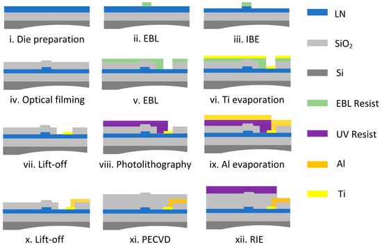
Figure 5.
Fabrication process of the modulation chip. EBL: electron beam lithography; IBE: ion beam etching; PECVD: plasma-enhanced chemical vapor deposition; RIE: reactive ion etching. UV: ultraviolet.
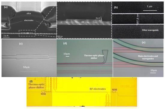
Figure 6.
Fabricated modulation chip. (a) Cross-sectional view of the waveguide in the modulation region. The inset shows an enlarged view of the LN waveguide. (b) SEM of the filter waveguide. (c) SEM of the MMI. (d) Micrograph of the thermo-optic phase shifter beside the waveguides. (e) Micrograph of the main electrodes and the waveguides at their crossings. (f) Micrograph of the fabricated modulation chip.
3. Results
Figure 7a–d show the measurement setups for static responses, Vπ, S11 and EO S21, and modulation spectrum, respectively. In Figure 7a, the light emitted by the laser (LD) (DL808, Crystalaser, Reno, NV, USA) passes through the polarization controller (PC) into the modulator under test (DUT) and then is output to the optical power meter (PM) (PM100D, Thorlabs, Newton, NJ, USA) with a sensor head (S120C, Thorlabs, Newton, New Jersey, United States) for power detection. A DC voltage power supply is adjusted to change the bias point. The maximum output power P1 and P0 are obtained with and without the modulator, respectively. The insertion loss (IL) of the modulation chip is IL (dB) = P0 (dBm) − P1 (dBm). The extinction ratio is ER (dB) = P1 (dBm) − P1’ (dBm), where P1’ represents the minimal output optical power across all DC bias statuses. The IL in the measuring system simulating the real application scenario of an atomic vapor cell is 7.6 dB, with a single-mode lensed fiber coupling in and a 2.5 cm diameter sensor head receiving the light. The measured ER is 30.94 dB, as shown in Figure 8a. The fluctuation remains within 0.1 dB in 30 s and within 1 dB in 30 min. The thermal resistor for DC tuning has a measured resistance of ~870 Ω, which slightly increases as the applied voltage and temperature rise. As Figure 8a demonstrates, the dissipation power to shift the bias point by half a wave is Pπ = 45 mW.
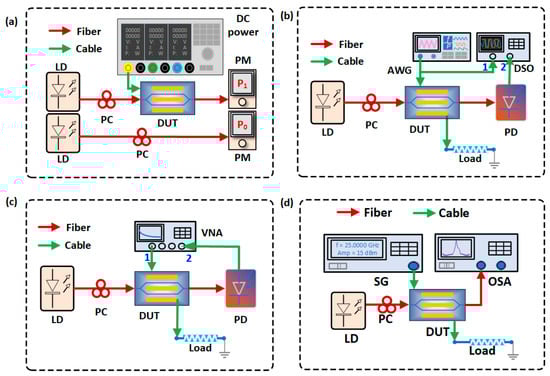
Figure 7.
Measurement setup for (a) static responses, (b) low-frequency Vπ, (c) EO S parameters and (d) modulation spectrum. LD: laser; PC: polarization controller; DUT: device under test; PM: optical power meter; VNA: vector network analyzer; AWG: arbitrary wave generator; SG: microwave signal generator; OSA: optical signal analyzer; Load: impedance-matched terminal; DSO: digital signal oscilloscope; PD: photodetector. Numbers “1” and “2” are port numbers of the equipment.
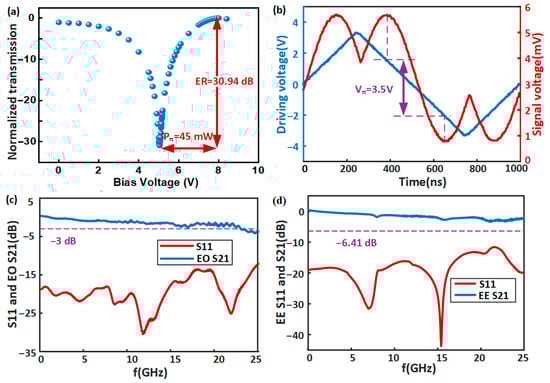
Figure 8.
Characterization of the fabricated modulation chip. (a) Static responses. ER and Pπ are indicated using red arrow line segments. (b) Vπ is determined with a 1 MHz triangular wave signal. (c) Measured S11 and EO S21. (d) Measured electrical S11 and S21.
Figure 7b shows the setup for measuring Vπ. A 1 MHz triangular signal generated by a low-frequency arbitrary wave generator (AWG) (DG4062, RIGOL, Suzhou, China) modulates the light from the LD at the DUT, which is terminated by a matching load. The modulated signal detected by a photodetector (PD) (DXM25DF, Thorlabs, Newton, NJ, USA) is delivered to the digital oscilloscope (DSO) (DS2202, RIGOL, Suzhou, China). The fabricated chip exhibits a Vπ of 3.5 V (Figure 8b), yielding a VπL of 1.8 Vcm with a modulation length of 5 mm. We note that the attenuation from the probe could not be de-embedded, so the Vπ was overestimated.
The setup for measuring S parameters is depicted in Figure 7c. Test signals from 10 MHz to 25 GHz deriving from the vector network analyzer (VNA) (PNA-X N5247A, Keysight, Santa Rosa, California, United Stated) through Port 1 flow into the DUT. The PD converts the modulated optical signals to electrical signals, which are received back at the VNA through Port 2. A matching load is attached to the DUT. After de-embedding the EO responses of the cables, probes and photodetector, the S11 and S21 of the DUT are extracted.
Figure 8c illustrates the measured EO bandwidth of 21.96 GHz. The measuring range is limited by the photodetector with a 3 dB bandwidth of 25 GHz. The electrical bandwidth is far beyond the testing range, as can be seen from Figure 8d, which indicates that the EO bandwidth is not primarily limited by the microwave loss. RF performance remains stable for hours as the chip is pressed flat and immobilized between two probes.
The modulators are packaged into two types, both bonded to a printed circuit board (PCB), with the input fibers adhered to the waveguide facet. In Figure 9a, the packaged modulator has an output fiber on the opposite side, while the modulator shown in Figure 9b is lens-integrated for optical output. The lens-integrated modulator is designed to couple with a collimator that connects to a receiving fiber. The IL is measured to be less than 18 dB, representing an upper limit owing to the unstable fixation within both the package and the alignment stage. Figure 9c,d show the low-frequency Vπ and EO frequency responses for the packaged modulators, respectively. The EO bandwidth is approximately 15 GHz, limited by the parasitic reactance introduced by PCB bonding. This is further evidenced by the electrical S21 measurement, which shows a roll-off to −6.41 dB at frequencies below 22 GHz (Figure 9e). Nonetheless, the measured Vπ matches that of the chip without deterioration.
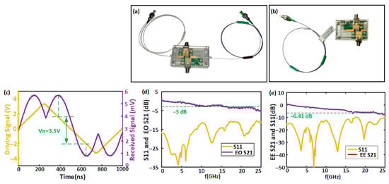
Figure 9.
The packaged modulators. (a) A photograph of the fiber-out-integrated modulator. (b) A photograph of the lens-out-integrated modulator. (c) Vπ determined with a 1 MHz triangular wave signal. (d) Measured S11 and EO S21. (e) Measured electrical S11 and S21.
In some applications, the modulated sidebands are used to induce atomic transitions in the atomic vapor cell. Figure 7d shows the setup for visualizing the modulation spectrum. The light from the LD passes the PC and is modulated by the DUT with the microwave from a source generator (SG). A matching load is attached to the DUT. An optical signal analyzer (OSA) (AQ6370C, YOKOGAWA, Musashino, 2 Chome Nakacho, Japan) displays the modulated spectrum from the DUT. The modulation spectrum is characterized as shown in Figure 10. The optical signal analyzer has a resolution limit of 0.040 nm near 795 nm, where a wavelength spacing of 1 nm corresponds to a frequency difference of ~474 GHz. Therefore, we used modulation frequencies up to 30 GHz for the commercial modulator and 32 GHz for our packaged modulator to distinguish the sidebands from the carrier at their peaks.
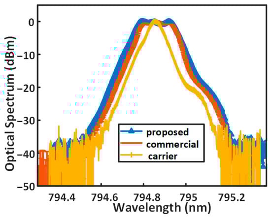
Figure 10.
Normalized measured spectrum from our packaged modulator with a 32 GH RF signal with no heating in Ti resistor and from the commercial modulator (MX800-LN-20, iXblue, Saint-Germain en Laye, Wallis and Futuna, France) with a 30 GHz RF signal at a bias volage of 5.2 V, compared to the carrier-only laser.
4. Discussion and Prospect
The IL can be further reduced by wet etching or rib-loaded waveguide patterning to obviate direct bombardment onto LN. An optimized lateral shift of the bent waveguide relative to the straight waveguide or using clothoid bends can also contribute to IL reduction [31,32]. Upon a further reduction in IL, or sufficient enhancement of the output power of the external modulated laser, the modulator is ready to be heterogeneously integrated onto the chip of 87Rb optical atomic clock. The VπL can be reduced by using smaller gaps and moving the waveguides towards the signal electrode. Moreover, transparent conductive oxide electrodes and T-rail microstructures can be implemented to break the trade-off between VπL and EO bandwidth [33,34]. A new way of reducing the Vπ is the use of a high dielectric constant (high-k) material cladding [35,36,37], since a cladding with a high dielectric constant strengthens the vertical electric field inside the electro-optic core for the same applied voltage, according to the continuity of normal components of the electric-displacement field. On the other hand, the EO bandwidth of packaged modulators is now constrained by the parasitic effect of the PCB bonding. A well-designed third-order Chebyshev filter section can compensate the parasitic parameters for impedance matching [38]. More work needs be performed in the future to investigate the mitigation method of high-frequency parasitic effects.
5. Conclusions
In conclusion, we proposed modulators for the 87Rb D1 line at about 795 nm. We provided guidelines for selecting the thickness of a LN film and designed strategies to minimize insertion losses. IL can be reduced through several methods: facet polishing and coating, widening the waveguide, using a single-taper edge coupler, and employing thick overcladding. These techniques help decrease scattering losses from the upper surface and interfaces, and increase alignment tolerance.
Although these designs are optimized for an NV modulator, they can be adapted to other spectra. Overall, the fabricated chip has the same level of performance as state-of-the-art devices, achieving an IL of 7.6 dB, an ER beyond 30 dB, a VπL of about 1.8 Vcm, and a 3 dB modulation bandwidth larger than 21 GHz.
We also demonstrated that the fabricated device is adaptable for packaging by presenting the measurement results of the encapsulated versions. While there was a deterioration in IL and electrical transmission, the packaged modulators still exhibited a modulation bandwidth of about 15 GHz, maintained the same VπL as the chip, and showed clear modulation sidebands. Table 3 compares our work with the most recent studies.
Table 3.
Key performance indicators of previous studies on VNIR modulators and our work.
This work provides practical guidance for enhancing TFLN modulators of the interference type. We believe that this advancement will significantly contribute to precision metrology, global positioning, and quantum processing.
Author Contributions
Conceptualization, Y.L.; methodology, X.L.; software, X.L. and R.S.; validation, X.L. and X.S.; formal analysis, X.L.; investigation, X.L.; resources, Y.L.; data curation, X.L.; writing—original draft preparation, X.L.; writing—review and editing, Z.C., Y.L., X.L., X.S., R.S., J.C. and S.Q.; visualization, X.L. and J.C.; supervision, Y.L. and Z.C.; project administration, Y.L.; funding acquisition, Y.L. All authors have read and agreed to the published version of the manuscript.
Funding
The APC was funded by State Key Laboratory of Photonics and Communications, Peking University, China.
Data Availability Statement
The raw data supporting the conclusions of this article will be made available by the authors on reasonable request.
Acknowledgments
The authors would like to thank Nanjing Nanzhi Advanced Optoelectronic Integrated Technology Research Institute Co., Ltd. for the on-chip fabrication and National Information Optoelectronics Innovation Center, China Information and Communication Technologies Group Corporation, for the packaging. During the preparation of this manuscript, the author used GenAI kimi for the purposes of precise scientific interpretation and polishing, as well as the formatting of the reference list. The authors have reviewed and edited the output and take full responsibility for the content of this publication.
Conflicts of Interest
The authors declare no conflicts of interest.
Abbreviations
The following abbreviations are used in this manuscript:
| EOM | Electro-optic modulator |
| EO | Electro-optic |
| NV | Near-visible |
| TFLN | Thin-film lithium niobate |
| LNOI | Lithium niobate on insulator |
| MZM | Mach–Zehnder modulator |
| IL | Insertion loss |
| ER | Extinction ratio |
| TE | Transverse electric |
| LN | Lithium niobate |
| RF | Radio frequency |
| DC | Direct current |
| TM | Transverse magnetic |
| MMI | Multimode interferometer |
| PECVD | Plasma-enhanced chemical vapor deposition |
| AR | Anti-reflection |
| EBL | Electron beam lithography |
| SEM | Scanning electron microscope |
| Vπ | Half-wave voltage |
| VπL | Half-wave voltage-length product |
| Pπ | Half-wave power |
| PCB | Printed circuit board |
References
- Sun, J.; Hao, Y.; Zhang, L.; Xu, J.; Zhu, S. Brief Review of Lithium Niobate Crystal and Its Applications. J. Synth. Cryst. 2020, 49, 947–964. [Google Scholar] [CrossRef]
- Abrahams, S.C.; Levinstein, H.J.; Reddy, J.M. Ferroelectric lithium niobate. 5. Polycrystal X-ray diffraction study between 24° and 1200 °C. J. Phys. Chem. Solids 1966, 27, 1019–1026. [Google Scholar] [CrossRef]
- Boyd, G.D.; Kasper, H.; McFee, J.H. Linear and Nonlinear Optical Properties of Ferroelectric Lithium Niobate. J. Appl. Phys. 1964, 35, 1662–1668. [Google Scholar]
- Turner, E.H. High-Frequency Electro-Optic Coefficients of Lithium Niobate. Appl. Phys. Lett. 1966, 8, 303–305. [Google Scholar] [CrossRef]
- Nassau, K.; Levinstein, H.J.; Loiacono, G.M. Ferroelectric Lithium Niobate Single Crystals: Growth and Domain Structure. J. Phys. Chem. Solids 1966, 27, 989–996. [Google Scholar] [CrossRef]
- Abrahams, S.C.; Hamilton, W.C.; Reddy, J.M. Ferroelectric Lithium Niobate. 4. Single-Crystal Neutron Diffraction Study at 24 °C. J. Phys. Chem. Solids 1966, 27, 1013–1018. [Google Scholar] [CrossRef]
- Wemple, S.H.; Didomenico, M.; Camlibel, I. Relationship between linear and quadratic electro-optic coefficients in LiNbO3, LiTaO3, and other oxy-gen-octahedra ferroelectrics based on direct measurement of spontaneous polarization. Appl. Phys. Lett. 1968, 12, 209–211. [Google Scholar] [CrossRef]
- Manzo, M.; Laurell, F.; Pasiskevicius, V.; Gallo, K. Lithium Niobate: The Silicon of Photonics! In Nano-Optics for Enhancing Light–Matter Interactions on a Molecular Scale; Di Bartolo, B., Collins, J., Eds.; NATO Science for Peace and Security Series B: Physics and Biophysics; Springer: Dordrecht, The Netherlands, 2013; pp. 485–500. [Google Scholar] [CrossRef]
- Lu, J.; Surya, J.B.; Liu, X.; Bruch, A.W.; Gong, Z.; Xu, Y.; Tang, H.X. Periodically Poled Thin-Film Lithium Niobate Microring Resonators with a Second-Harmonic Generation Efficiency of 250,000%/W. Optica 2019, 6, 1455–1460. [Google Scholar] [CrossRef]
- Ghione, G. Semiconductor Devices for High-Speed Optoelectronics; Cambridge University Press: Cambridge, UK, 2009. [Google Scholar]
- Wooten, E.L.; Kissa, K.M.; Yi-Yan, A.; Murphy, E.J.; Lafaw, D.A.; Hallemeier, P.F.; Maack, D.; Attanasio, D.V.; Fritz, D.J.; McBrien, G.J.; et al. A Review of Lithium Niobate Modulators for Fiber-Optic Communications Systems. IEEE J. Sel. Top. Quantum Electron. 2000, 6, 69–82. [Google Scholar] [CrossRef]
- Poberaj, G.; Hu, H.; Sohler, W.; Günter, P. Lithium Niobate on Insulator (LNOI) for Micro-Photonic Devices. Laser Photonics Rev. 2012, 6, 488–503. [Google Scholar] [CrossRef]
- Wang, C.; Zhang, M.; Chen, X.; Bertrand, M.; Shams-Ansari, A.; Chandrasekhar, S.; Winzer, P.; Lončar, M. Integrated Lithium Niobate Electro-Optic Modulators Operating at CMOS-Compatible Voltages. Nature 2018, 562, 101–104. [Google Scholar] [CrossRef]
- Wang, C.; Zhang, M.; Stern, B.; Lipson, M.; Lončar, M. Nanophotonic Lithium Niobate Electro-Optic Modulators. Opt. Express 2018, 26, 1547–1555. [Google Scholar] [CrossRef] [PubMed]
- Zhang, M.; Wang, C.; Kharel, P.; Zhu, D.; Lončar, M. Integrated Lithium Niobate Electro-Optic Modulators: When Performance Meets Scalability. Optica 2021, 8, 652–667. [Google Scholar] [CrossRef]
- Bandi, T.N. A Comprehensive Overview of Atomic Clocks and Their Applications. Biol. Eng. Med. Sci. Rep. 2023, 9, 1–10. [Google Scholar] [CrossRef]
- Ludlow, A.D.; Boyd, M.M.; Ye, J.; Peik, E.; Schmidt, P.O.; Katori, H.; Oates, C.W.; Diddams, S.A.; Le Coq, Y.; Takamoto, M.; et al. Optical Atomic Clocks. Rev. Mod. Phys. 2015, 87, 637–701. [Google Scholar] [CrossRef]
- Liu, Z.; Wang, Z.; Qin, X.; Zhu, C.; Li, M.; Zhang, J.; Chen, X.; Zhang, S.; Zhang, J.; Liu, H.; et al. Turn-Key Voigt Optical Frequency Standard. Photonics Res. 2025, 13, 1083–1093. [Google Scholar] [CrossRef]
- Romero-García, S.; Merget, F.; Zhong, F.; Finkelstein, H.; Witzens, J. Silicon Nitride CMOS-Compatible Platform for Integrated Photonics Applications at Visible Wavelengths. Opt. Express 2013, 21, 14036–14046. [Google Scholar] [CrossRef] [PubMed]
- Yang, F.; Fang, X.; Chen, X.; Zhu, L.; Li, Y.; Zhang, J.; Wang, Y.; Zhang, M.; Wang, H.; Zhang, J.; et al. Monolithic Thin-Film Lithium Niobate Electro-Optic Modulator with Over 110 GHz Bandwidth. Chin. Opt. Lett. 2022, 20, 022502. [Google Scholar] [CrossRef]
- Ummethala, S.; Kemal, J.N.; Alam, A.S.; Lauermann, M.; Kuzmin, A.; Kutuvantavida, Y.; Nandam, S.H.; Hahn, L.; Elder, D.L.; Dalton, L.R.; et al. Hybrid Electro-Optic Modulator Combining Silicon Photonic Slot Waveguides with High-k Radio-Frequency Slotlines. Optica 2021, 8, 511–519. [Google Scholar] [CrossRef]
- Zhu, D.; Shao, L.; Yu, M.; Cheng, R.; Desiatov, B.; Xin, C.J.; Hu, Y.; Holzgrafe, J.; Ghosh, S.; Shams-Ansari, A.; et al. Integrated Photonics on Thin-Film Lithium Niobate. Adv. Opt. Photonics 2021, 13, 242–352. [Google Scholar] [CrossRef]
- Çelik, Ö.T.; Sarabalis, C.J.; Mayor, F.M.; Patel, P.; Safavi-Naeini, A.H. High-Bandwidth CMOS-Voltage-Level Electro-Optic Modulation of 780 nm Light in Thin-Film Lithium Niobate. Opt. Express 2022, 30, 23177–23186. [Google Scholar] [CrossRef] [PubMed]
- Xue, S.; Shi, Z.; Ling, J.; Gao, Z.; Hu, Q.; Zhang, K.; Valentine, G.; Wu, X.; Staffa, J.; Javid, U.A.; et al. Full-Spectrum Visible Electro-Optic Modulator. Optica 2023, 10, 125–126. [Google Scholar] [CrossRef]
- Valdez, F.; Mere, V.; Mookherjea, S. 100 GHz Bandwidth, 1 V Integrated Electro-Optic Mach–Zehnder Modulator at Near-IR Wavelengths. Optica 2023, 10, 578–584. [Google Scholar] [CrossRef]
- Assumpção, D.; Renaud, D.; Shams-Ansari, A.; Sinclair, A.; Lončar, M. Sub-1 V Near-Infrared Thin-Film Lithium Niobate Modulator for High-Speed Visible Communication. In Proceedings of the 2024 Optical Fiber Communications Conference and Exhibition (OFC), San Diego, CA, USA, 24–28 March 2024. [Google Scholar] [CrossRef]
- Renaud, D.; Assumpção, D.R.; Joe, G.; Shams-Ansari, A.; Sinclair, A.; Lončar, M. Sub-1 Volt and High-Bandwidth Visible to Near-Infrared Electro-Optic Modulators. Nat. Commun. 2023, 14, 1496. [Google Scholar] [CrossRef]
- Kawaguchi, T.; Miyasaka, M.; Shimada, J.; Ohtani, Y.; Takeda, H.; Kurita, S. Measurement of Dispersion of Effective Electro-Optic Coefficients r13E and r33E of Non-Doped Congruent LiNbO3 Crystal. Jpn. J. Appl. Phys. 2008, 47, 5503–5507. [Google Scholar] [CrossRef]
- Chen, G.; Lin, H.-L.; Ng, J.D.; Danner, A.J. Integrated Electro-Optic Modulator in Z-Cut Lithium Niobate Thin Film with Vertical Structure. IEEE Photonics Technol. Lett. 2021, 33, 1285–1288. [Google Scholar] [CrossRef]
- Thomson, D.J.; Hu, Y.; Reed, G.T.; Littlejohns, C.G.; Mashanovich, G.Z.; Gardes, F.Y.; Nedeljkovic, M.; Soler Penades, J.; Alonso-Ramos, C.; Ortega-Moñux, A.; et al. Low-Loss MMI Couplers for High-Performance MZI Modulators. IEEE Photonics Technol. Lett. 2010, 22, 1485–1487. [Google Scholar] [CrossRef]
- Rahman, B.M.A.; Leung, D.M.H.; Obayya, S.S.A.; Grattan, K.T.V. Numerical Analysis of Bent Waveguides: Bending Loss, Transmission Loss, Mode Coupling, and Polarization Coupling. Appl. Opt. 2008, 47, 2961–2970. [Google Scholar] [CrossRef]
- Fujisawa, T.; Makino, S.; Sato, T.; Saitoh, K. Low-Loss, Compact, and Fabrication-Tolerant Si-Wire 90° Waveguide Bend Using Clothoid and Normal Curves for Large-Scale Photonic Integrated Circuits. Opt. Express 2017, 25, 9150–9159. [Google Scholar] [CrossRef]
- Meng, X.; Yuan, C.; Cheng, X.; Yuan, S.; Shang, C.; Pan, A.; Qu, Z.; Wang, X.; Wang, J.; Zhang, P.; et al. Thin-Film Lithium Niobate Modulators with Ultra-High Modulation Efficiency. Laser Photonics Rev. 2024, 18, 2400809. [Google Scholar] [CrossRef]
- Kharel, P.; Reimer, C.; Luke, K.; He, L.; Zhang, M. Breaking Voltage–Bandwidth Limits in Integrated Lithium Niobate Modulators Using Micro-Structured Electrodes: Erratum. Optica 2021, 8, 1218. [Google Scholar] [CrossRef]
- Alam, A.S.; Aitchison, J.S. Optimization of a Broadband Lithium Niobate–Barium Titanate Hybrid Modulator with Low Half-Wave-Voltage–Length Product. IEEE Photonics J. 2023, 15, 6602407. [Google Scholar] [CrossRef]
- Alam, A.S.; Aitchison, J.S. Low Half-Wave-Voltage Lithium Niobate Modulator Using High-k Dielectric Material Cladding. In 2022 Optica Advanced Photonics Congress; Optica Publishing Group: Washington, DC, USA, 2022. [Google Scholar]
- Alam, A.S. High-Speed and Power-Efficient Integrated Electro-Optic Modulators. Ph.D. Thesis, University of Toronto, Toronto, ON, Canada, 2025. [Google Scholar]
- Cui, G.; Yuan, W.; Liu, J.; Cui, X.; Liu, X. Extraction and Compensation of Bonding Wires Parasitic Parameter. In Proceedings of the 2022 Cross Strait Radio Science & Wireless Technology Conference (CSRSWTC), Beijing, China, 17–18 December 2022; pp. 1–3. [Google Scholar] [CrossRef]
- Desiatov, B.; Shams-Ansari, A.; Zhang, M.; Wang, C.; Lončar, M. Ultra-Low-Loss Integrated Visible Photonics Using Thin-Film Lithium Niobate. Optica 2019, 6, 380–384. [Google Scholar] [CrossRef]
Disclaimer/Publisher’s Note: The statements, opinions and data contained in all publications are solely those of the individual author(s) and contributor(s) and not of MDPI and/or the editor(s). MDPI and/or the editor(s) disclaim responsibility for any injury to people or property resulting from any ideas, methods, instructions or products referred to in the content. |
© 2025 by the authors. Licensee MDPI, Basel, Switzerland. This article is an open access article distributed under the terms and conditions of the Creative Commons Attribution (CC BY) license (https://creativecommons.org/licenses/by/4.0/).