Optimization of Voltage Requirements in Electro-Optic Polarization Controllers for High-Speed QKD Systems


Abstract
1. Introduction
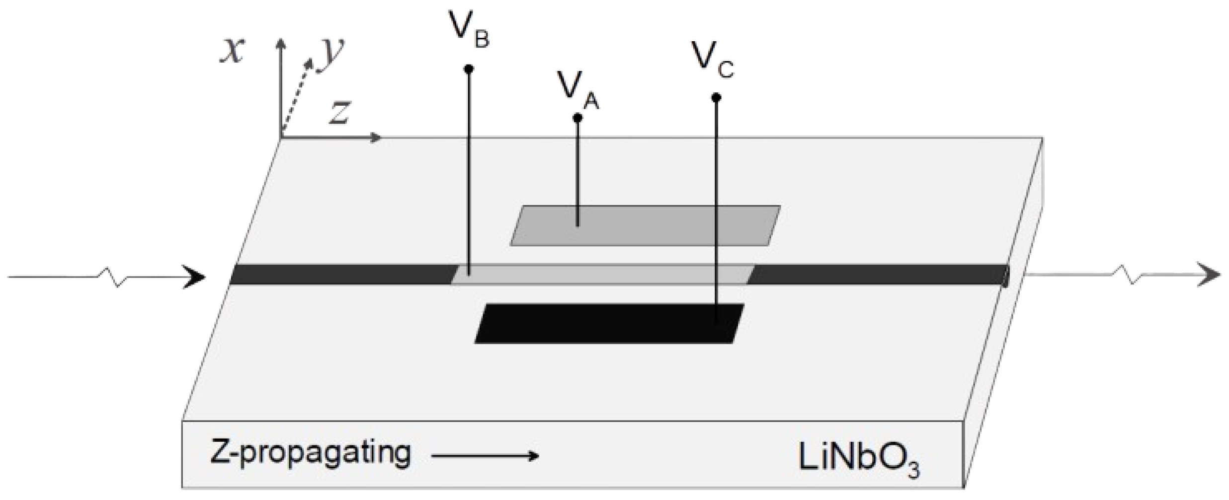
2. EPC Description
3. Optimizing Domains of the Wave-Plate Phase Delay and the Fast Axis Orientation
3.1. Optimization Objectives
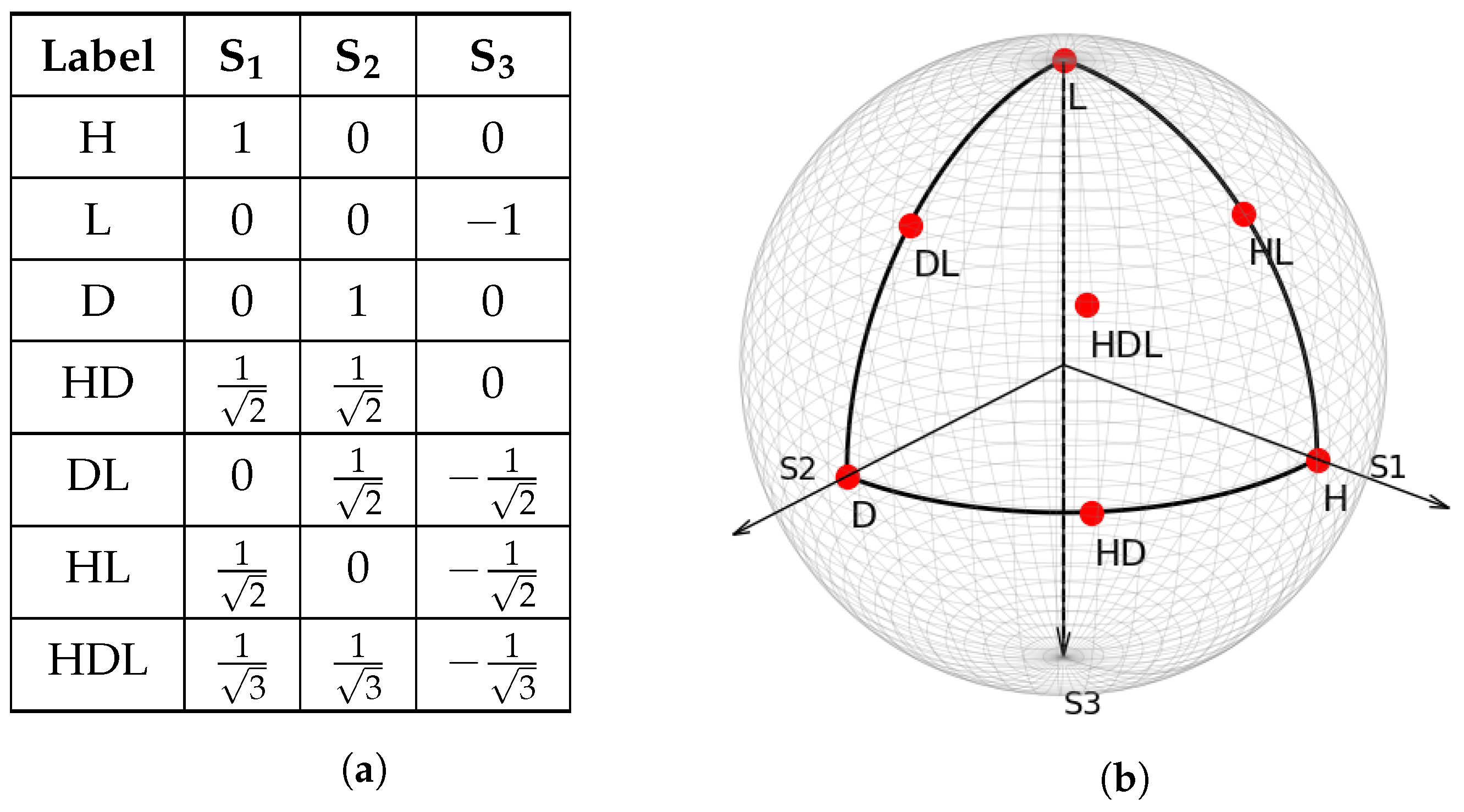
- Minimization of the SOP error in Stokes space.
- Minimization of the absolute maximum voltage deviation from a reference voltage value.
- Minimization of the absolute maximum voltage jump between the SOPs required by a QKD protocol.
3.2. Algorithm Implementation
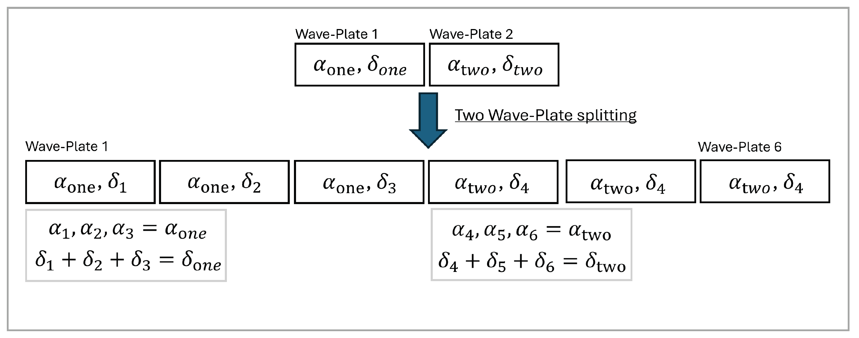
3.3. Wave-Plate Splitting
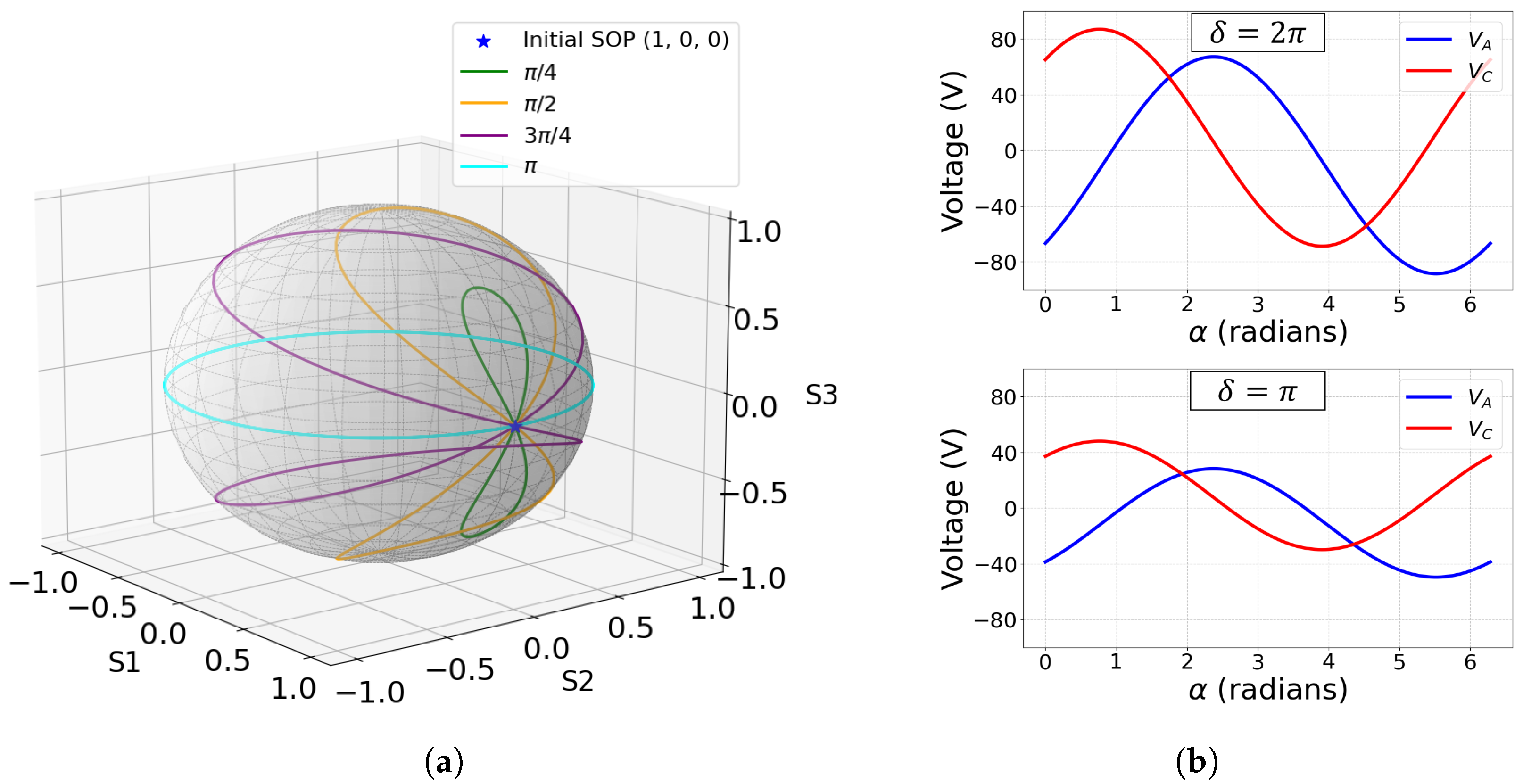
4. Simulation Results for Voltage Optimization
4.1. Optimization Surrounding Bias Voltage Points
4.2. Optimization Surrounding Zero Volts
4.3. Voltage Swings
5. Discussion and Conclusions
Author Contributions
Funding
Institutional Review Board Statement
Informed Consent Statement
Data Availability Statement
Conflicts of Interest
References
- Boudot, F.; Gaudry, P.; Guillevic, A.; Heninger, N.; Thomé, E.; Zimmermann, P. The State of the Art in Integer Factoring and Breaking Public-Key Cryptography. IEEE Secur. Priv. 2022, 20, 80–86. [Google Scholar] [CrossRef]
- Wei, S.H.; Jing, B.; Zhang, X.Y.; Liao, J.Y.; Yuan, C.Z.; Fan, B.Y.; Lyu, C.; Zhou, D.L.; Wang, Y.; Deng, G.W.; et al. Towards real-world quantum networks: A review. Laser Photon. Rev. 2022, 16, 2100219. [Google Scholar] [CrossRef]
- Muga, N.; Ramos, M.; Mantey, S.; Silva, N.; Pinto, A. FPGA-assisted state-of-polarization generation for polarization-encoded optical communications. IET Optoelectron. 2020, 14, 350–355. [Google Scholar] [CrossRef]
- Liao, S.K.; Cai, W.Q.; Liu, W.Y.; Zhang, L.; Li, Y.; Ren, J.G.; Yin, J.G.; Shen, Q.; Cao, Y.; Li, Z.P.; et al. Satellite-to-ground quantum key distribution. Nature 2017, 549, 43–47. [Google Scholar] [CrossRef] [PubMed]
- Liao, S.K.; Yong, H.L.; Liu, C.; Shentu, G.L.; Li, D.D.; Lin, J.; Dai, H.; Zhao, S.Q.; Li, B.; Guan, J.Y.; et al. Long-distance free-space quantum key distribution in daylight towards inter-satellite communication. Nat. Photonics 2017, 11, 509–513. [Google Scholar] [CrossRef]
- Agnesi, C.; Avesani, M.; Calderaro, L.; Stanco, A.; Foletto, G.; Zahidy, M.; Scriminich, A.; Vedovato, F.; Vallone, G.; Villoresi, P. Simple quantum key distribution with qubit-based synchronization and a self-compensating polarization encoder. Optica 2020, 7, 284–290. [Google Scholar] [CrossRef]
- Mantey, S.; Silva, N.; Pinto, A.; Muga, N. Design and implementation of a polarization-encoding system for quantum key distribution. J. Opt. 2024, 26, 075704. [Google Scholar] [CrossRef]
- Williams, J.; Suchara, M.; Zhong, T.; Qiao, H.; Kettimuthu, R.; Fukumori, R. Implementation of quantum key distribution and quantum clock synchronization via time bin encoding. Proc. SPIE 2021, 11699, 16–25. [Google Scholar]
- Boaron, A.; Korzh, B.; Houlmann, R.; Boso, G.; Rusca, D.; Gray, S.; Li, M.J.; Nolan, D.; Martin, A.; Zbinden, H. Simple 2.5 GHz time-bin quantum key distribution. Appl. Phys. Lett. 2018, 112, 171108. [Google Scholar] [CrossRef]
- Liang, W.Y.; Wang, S.; Li, H.W.; Yin, Z.Q.; Chen, W.; Yao, Y.; Huang, J.Z.; Guo, G.C.; Han, Z.F. Proof-of-principle experiment of reference-frame-independent quantum key distribution with phase coding. Sci. Rep. 2014, 4, 1–6. [Google Scholar] [CrossRef]
- Bennett, C.H.; Brassard, G. Quantum Cryptography: Public Key Distribution and Coin Tossing. In Proceedings of the IEEE International Conference on Computers, Systems and Signal Processing, Bangalore, India, 10–12 December 1984; pp. 175–179. [Google Scholar]
- Yan, Z.; Meyer-Scott, E.; Bourgoin, J.P.; Higgins, B.L.; Gigov, N.; MacDonald, A.; Hübel, H.; Jennewein, T. Novel High-Speed Polarization Source for Decoy-State BB84 Quantum Key Distribution Over Free Space and Satellite Links. J. Light. Technol. 2013, 31, 1399–1408. [Google Scholar] [CrossRef]
- Liu, X.; Liao, C.; Tang, Z.; Wang, J.; Wei, Z.; Liu, S. Polarization coding and decoding by phase modulation in polarizing sagnac interferometers. Proc. SPIE 2007, 6827, 68270I. [Google Scholar]
- Duplinskiy, A.; Ustimchik, V.; Kanapin, A.; Kurochkin, V.; Kurochkin, Y. Low loss QKD optical scheme for fast polarization encoding. Opt. Express 2017, 25, 28886. [Google Scholar] [CrossRef]
- Wang, J.; Qin, X.; Jiang, Y.; Wang, X.; Chen, L.; Zhao, F.; Wei, Z.; Zhang, Z. Experimental demonstration of polarization encoding quantum key distribution system based on intrinsically stable polarization-modulated units. Opt. Express 2016, 24, 8302–8309. [Google Scholar] [CrossRef] [PubMed]
- Comandar, L.C.; Fröhlich, B.; Lucamarini, M.; Patel, K.A.; Sharpe, A.W.; Dynes, J.F.; Yuan, Z.L.; Penty, R.V.; Shields, A.J. Room temperature single-photon detectors for high bit rate quantum key distribution. Appl. Phys. Lett. 2014, 104, 021101. [Google Scholar] [CrossRef]
- Chen, S.; You, L.; Zhang, W.; Yang, X.; Li, H.; Zhang, L.; Wang, Z.; Xie, X. Dark counts of superconducting nanowire single-photon detector under illumination. Opt. Express 2015, 23, 10786–10793. [Google Scholar] [CrossRef] [PubMed]
- Xiao-Bao, L.; Chang-Jun, L.; Zhi-Lie, T.; Jin-Dong, W.; Song-Hao, L. Quantum Key Distribution System with Six Polarization States Encoded by Phase Modulation. Chin. Phys. Lett. 2008, 25, 3856. [Google Scholar] [CrossRef]
- Xi, L.; Zhang, X.; Tian, F.; Tang, X.; Weng, X.; Zhang, G.; Li, X.; Xiong, Q. Optimizing the operation of LiNbO3-based multistage polarization controllers through an adaptive algorithm. IEEE Photonics J. 2010, 2, 195–202. [Google Scholar]
- Shan, L.; Lu, Q.; Sun, P.; Zhang, X.; Xi, L.; Xiao, X. Calibration of LiNbO3- based polarization controller with simplified principle and RMSProp algorithm. In Proceedings of the 2023 Asia Communications and Photonics Conference/2023 Photonics and Optoelectronics Meetings (ACP/POEM), Wuhan, China, 4–7 November 2023; pp. 1–3. [Google Scholar]
- Garcia, J.D.; Amaral, G.C. An optimal polarization tracking algorithm for Lithium-Niobate-based polarization controllers. In Proceedings of the 2016 IEEE Sensor Array and Multichannel Signal Processing Workshop (SAM), Rio de Janeiro, Brazil, 10–13 July 2016. [Google Scholar]
- Hou, Q.; Yuan, X.; Zhang, Y.; Zhang, J. Endless polarization stabilization control for optical communication systems. Chin. Opt. Lett. 2014, 12, 110603. [Google Scholar]
- Xavier, G.B.; Walenta, N.; Vilela de Faria, G.; Temporão, G.P.; Gisin, N.; Zbinden, H.; von der Weid, J.P. Experimental polarization encoded quantum key distribution over optical fibres with real-time continuous birefringence compensation. N. J. Phys. 2009, 11, 045015. [Google Scholar] [CrossRef]
- Costa, H.; Muga, N.J.; Silva, N.A.; Pinto, A.N. Advanced Algorithms for Optimization of QKD Encoding Subsystems. In Proceedings of the International Conference on Applications of Optics and Photonics—AOP2014, Aveiro, Portugal, 16–19 July 2024. [Google Scholar]
- Gunantara, N. A review of multi-objective optimization: Methods and its applications. Cogent Eng. 2018, 5, 1502242. [Google Scholar] [CrossRef]
- Deb, K.; Pratap, A.; Agarwal, S.; Meyarivan, T. A fast and elitist multiobjective genetic algorithm: NSGA-II. IEEE Trans. Evol. Comput. 2002, 6, 182–197. [Google Scholar] [CrossRef]
- van Haasteren, A.; van der Tol, J.; van Deventer, M.; Frankena, H. Modeling and characterization of an electrooptic polarization controller on LiNbO3. J. Light. Technol. 1993, 11, 1151–1157. [Google Scholar] [CrossRef]
- EOSPACE. Polarization Controller Calibration Data; User’s Manual; EOSPACE: Redmond, WA, USA, 2014. [Google Scholar]
- Goldstein, D.H. Polarized Light, 3rd ed.; CRC Press: Boca Raton, FL, USA, 2011. [Google Scholar]
- Blank, J.; Deb, K. pymoo: Multi-Objective Optimization in Python. IEEE Access 2020, 8, 89497–89509. [Google Scholar] [CrossRef]
- Salvestrini, J.P.; Guilbert, L.; Fontana, M.; Abarkan, M.; Gille, S. Analysis and Control of the DC Drift in LiNbO3-Based Mach–Zehnder Modulators. J. Light. Technol. 2011, 29, 1522–1534. [Google Scholar] [CrossRef]
Disclaimer/Publisher’s Note: The statements, opinions and data contained in all publications are solely those of the individual author(s) and contributor(s) and not of MDPI and/or the editor(s). MDPI and/or the editor(s) disclaim responsibility for any injury to people or property resulting from any ideas, methods, instructions or products referred to in the content. |
© 2025 by the authors. Licensee MDPI, Basel, Switzerland. This article is an open access article distributed under the terms and conditions of the Creative Commons Attribution (CC BY) license (https://creativecommons.org/licenses/by/4.0/).
Share and Cite
Costa, H.F.; Pinto, A.N.; Muga, N.J. Optimization of Voltage Requirements in Electro-Optic Polarization Controllers for High-Speed QKD Systems. Photonics 2025, 12, 267. https://doi.org/10.3390/photonics12030267
Costa HF, Pinto AN, Muga NJ. Optimization of Voltage Requirements in Electro-Optic Polarization Controllers for High-Speed QKD Systems. Photonics. 2025; 12(3):267. https://doi.org/10.3390/photonics12030267
Chicago/Turabian StyleCosta, Hugo Filipe, Armando Nolasco Pinto, and Nelson Jesus Muga. 2025. "Optimization of Voltage Requirements in Electro-Optic Polarization Controllers for High-Speed QKD Systems" Photonics 12, no. 3: 267. https://doi.org/10.3390/photonics12030267
APA StyleCosta, H. F., Pinto, A. N., & Muga, N. J. (2025). Optimization of Voltage Requirements in Electro-Optic Polarization Controllers for High-Speed QKD Systems. Photonics, 12(3), 267. https://doi.org/10.3390/photonics12030267