Article

Illumination Field Uniformity Correction by Novel Finger Arrays for Lithography Illumination System

1
School of Optical and Electronic Information, Huazhong University of Science and Technology, Wuhan 430074, China
2
Institute of Optics and Electronics, Chinese Academy of Sciences, Chengdu 610209, China
3
University of Chinese Academy of Sciences, Beijing 100049, China
*
Author to whom correspondence should be addressed.
Photonics 2024, 11(7), 661; https://doi.org/10.3390/photonics11070661
Submission received: 15 May 2024 / Revised: 16 June 2024 / Accepted: 10 July 2024 / Published: 15 July 2024
(This article belongs to the Section Optoelectronics and Optical Materials)

Abstract

:
In order to correct the integrated nonuniformity of a lithographic illumination field, a high-precision uniformity correction method for an advanced lithographic illumination system is proposed. The method adopts the opaque finger array structure and improves correction ability and accuracy by optimizing the arrangement and structure of the unit without changing the width of each unit. The correction accuracy is expressed as the percentage of the corrected integrated nonuniformity. Through theoretical analysis and simulation, it can be seen that the correction accuracy of a staggered finger array is better than 0.22%. When staggered and layered, the correction accuracy of a finger array is better than 0.14%, which is better than that of a non-layered finger array. When staggered, layered, and chamfered of each unit, the correction accuracy of the finger array structure is better than 0.12%.

1. Introduction

In the integrated circuit manufacturing process, the most critical link is the lithography technology, which can form precise patterns on the silicon substrate [1]. The internal structure of the lithographic apparatus is complex. The exposure optical system is the core system of the lithographic apparatus, and the illumination system is one of the core subsystems of the exposure optical system. The main function of the illumination system is to provide an illumination field with a specific ray angle spectrum and intensity distribution for projection objective imaging [2]. Previous work has shown that the characteristics of the illumination of a lithography tool can affect resolution and alignment at the wafer [3]. The illuminator has to deliver invariant illumination across the reticle field [4]. After shaping and homogenizing the light from the light source, the uniform illumination field illuminates the mask, and the pattern of the mask is uniformly exposed to the wafer through the projection objective lens. In a lithography system, the nonuniformity of exposure dose on the mask and silicon wafer will lead to the difficulty of controlling the pattern linewidth, and the linewidth nonuniformity will affect the resolution, thus affecting the Critical Dimension (CD) of the lithographic apparatus [5]. The Critical Dimension (CD) is the key index of the lithography apparatus. In step-scanning lithography, the exposure dose at any point in the silicon wafer is the integrated nonuniformity of the illumination field in the scanning direction, so the integrated nonuniformity of the illumination field in the scanning direction becomes an important factor affecting Critical Dimension Uniformity (CDU) [6].
With the advancement of lithography process nodes, the requirements for CDU, which has an important impact on the resolution of the lithographic apparatus, are gradually becoming stricter [7]. Meeting a specific CDU roadmap becomes more and more difficult as different budget components affecting CDU fail to meet their requirements [8]. There are different contributors which impact the total CDU: mask CD uniformity, scanner and lens fingerprint, the resist process, wafer topography, the mask error enhancement factor, etc. [9]. This also means that the requirements for the integrated nonuniformity of the illumination field are more stringent. In the design of the lithographic apparatus illumination system, it is necessary to evaluate and correct the uniformity of the illumination field with different numerical apertures and different illumination modes. By adjusting the dose distribution on the illumination system to compensate for various sources of error, it is possible to more effectively control the non-uniform distribution of exposure doses, thereby improving overall exposure uniformity.
In order to ensure the uniformity of the exposure dose of the lithographic apparatus, the step-scanning lithography system adopts uniform illumination and trapezoidal illumination in the scanning direction on the wafer [10]. To further reduce the pulse quantization effect, flat-top Gaussian illumination can be used in the scanning direction. Compared to trapezoidal illumination, flat-top Gaussian light can maintain fixed slit edges without enhancing the pulse quantization effect [11]. To some extent, flat-top Gaussian illumination can improve the uniformity of the illumination field, but it still cannot meet the higher level of uniformity requirements. Under the limitations of specific process-level errors and adjustment errors, it is necessary to further add illumination field-homogenizing devices to achieve the uniformization of the illumination field. Currently, the main homogenizing units include light rod integrators [12] and microlens arrays [13,14,15], which can initially achieve the uniformization of the illumination field. In order to carry out a more in-depth treatment of the uniformity of the illumination field, it is necessary to design specific uniformity correction devices to correct the uniformity of the illumination field.
The uniformity correction of the lithography illumination system can be achieved by adjusting the grayscale compensation of the transmittance distribution or by optimizing the dose distribution of the edge field. Among them, grayscale compensation methods include static grayscale compensation [16] and dynamic grayscale compensation [17]. The static grayscale compensation method achieves precise control of the intensity of the illumination field at different positions by setting a specific transmittance distribution. However, this method can only correct specific illumination field distributions and lacks flexibility. The dynamic gray compensation method uses two devices with different transmission distributions and changes the relative position to achieve a different transmission distribution, and then controls the illumination field distribution at the corresponding position. The proposed method can achieve uniformity correction in different illumination modes and has a higher flexibility than the static gray compensator. However, the problem of the dynamic grayscale board is the lack of an ability for uniformity correction. The finger array correction method [18,19,20] inserts an opaque array structure into the illumination field, blocks the light energy at the edge, and then adjusts the distribution of the edge of the illumination field to realize the correction of the uniformity of the illumination field. Compared with the gray compensation method, the finger array correction method has a higher correction accuracy and flexibility. It is suitable for the lithography illumination system at 65 nm and higher nodes and can correct the uniformity of the illumination field to a higher level. The smaller the width of the unit of the finger array correction device is, the higher the correction accuracy will be, and, accordingly, the more difficult the arrangement of the corresponding driving unit will be. Moreover, the area of the unit inserted into the illumination field is related to the coherence factor of the lithographic apparatus illumination system, so the higher the number of units, the more the workload of the calculation, and the lower the work efficiency. In order to improve the correction accuracy, the existing finger array structure would have to greatly increase the number of units, which would increase the difficulty of the work.
The large number of units in the finger array brings great challenges to the arrangement and calculation of control units. Therefore, this paper adopts the appropriate width of the unit body and ensures that under the same width of the unit body, the staggered and layered arrangement and the change of the front-end structure of the unit body are adopted to further improve the correction ability and accuracy. The improved correctors can significantly improve the integrated uniformity, and the correction accuracy is better than 0.14% under different illumination modes.

2. Theoretical Analysis

2.1. Principle of Uniformity of Illumination Field

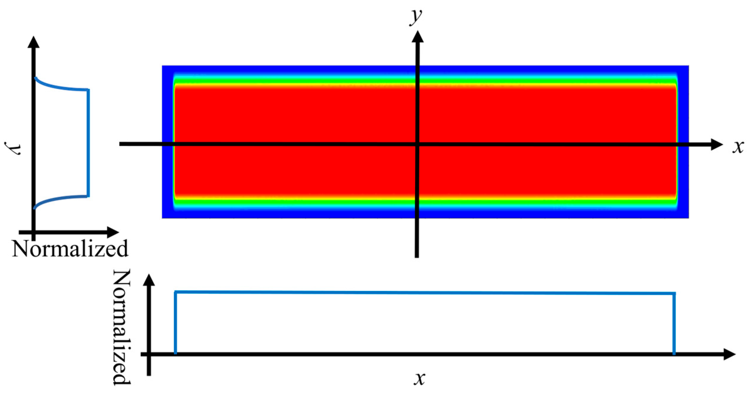
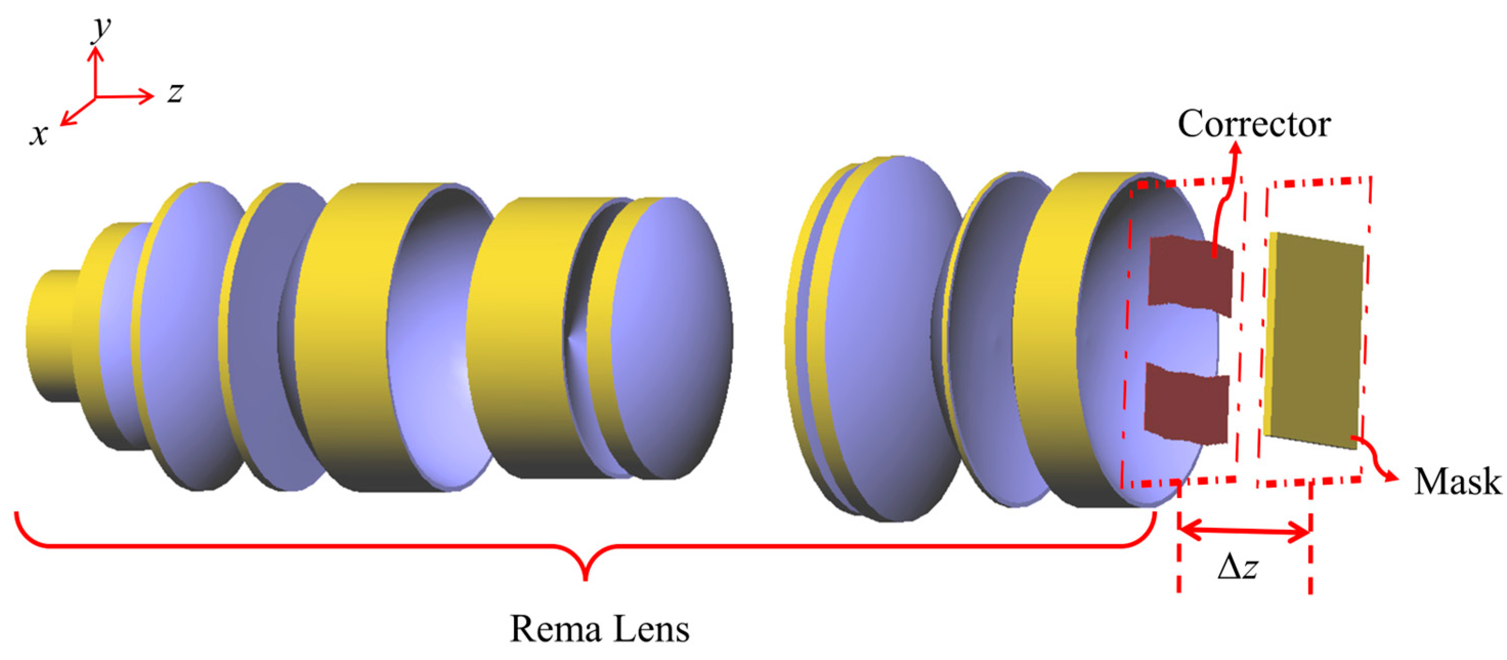
Figure 1 shows a simplified lithography exposure optical system. The illumination system consists of a laser emitter, beam expander, diffractive optical units (DOEs), a zoom lens, pupil shaping unit, condenser, uniform light rod, scanning silt, rema lens, corrector and a mask. The units that contribute to illumination field uniformity are the uniform light rod and corrector. On the mask plane, an illumination field is generated with a flat-top Gaussian distribution in the scanning direction (y direction) and a uniform distribution in the non-scanning direction (x direction). The illumination field distribution on the mask plane is shown in Figure 2.
In a step-scanning lithographic apparatus, the exposure metrology uniformity of a silicon wafer plane is determined by the integrated uniformity of the illumination field in the scanning direction. Assuming that the light intensity of the illumination field on the mask plane at the coordinate point (x,y) is I(x,y), then, after integrating the illuminated illumination field along the scanning direction, the equation for the integrated light intensity in the scanning direction is as follows:
I x = d / 2 d / 2 I x , y d y
where d is the width of the scanning direction (y direction) of the illumination field.
Among them, the x direction is the non-scanning direction, and the light intensity is uniformly distributed; the y direction is the scanning direction, and the light intensity has a flat-top Gaussian distribution, as shown in Figure 2.
The uniformity of the illumination field in the scanning direction can be characterized by the integrated nonuniformity formula. The smaller the integrated nonuniformity value is, the better the uniformity is. The illumination-integrated nonuniformity (IINU) formula [17] can be expressed as follows:
I I N U = m a x I x m i n I x m a x I x + m i n I x × 100 %
where max() and min() represent the maximum and minimum values, respectively.
To achieve a higher resolution and greater depth of focus, off-axis illumination techniques are required. By controlling the zoom lens group and DOEs, different illumination modes can be realized, including the conventional mode, annular mode, and quadrupole mode, as shown in Figure 3. Under different illumination modes, the coherence factor is different, and the distribution of the illumination field is different. The area and coherence factor of the unit inserted into the illumination field are different, so the movement of each unit of the finger array needs to be calculated according to the coherence factor of different illumination modes.

2.2. Principle of Uniformity Correction for Finger Array

The principal light of each field point on the mask plane is parallel to the optical axis, and the aperture angle is consistent. Therefore, on the correction plane at a certain distance from the mask plane, the sub-pupil distribution formed by each field point is consistent, and the relative position with the field point is also consistent. The light intensity distribution on the mask plane is the superposition of the pupil light intensity of all field points.
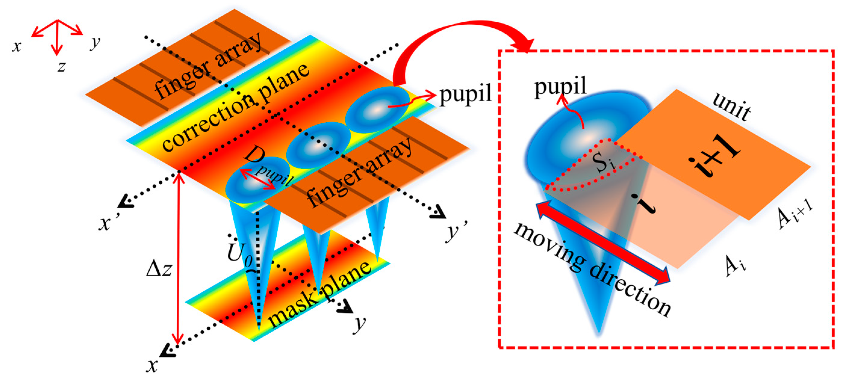
As shown in Figure 4, the distance between the mask plane and the correction plane is Δz, and so the relationship between the pupil diameter Dpupil of the correction plane and Δz [20] is as follows:
D p u p i l = 2 t a n U 0 Δ z
where U0 is half of the aperture angle at the mask plane, associated with the coherence factor σout, and can be expressed as follows:
U 0 = a r c s i n N A p o σ o u t
The light intensity at any point (x,y) of the illumination field on the mask plane is I(x,y), and the light intensity corresponding to any point on the correction plane is as follows:
I c x , y = I x , y i = 1 n S i I x , y / π D p u p i l / 2 2 d S
where, Si is the opaque area in which a single unit Ai of the finger array is inserted into the pupil, and n is the number of the finger array. The integrated light intensity Ic of the illumination field corrected by the finger array along the scanning direction is as follows:
I c = d / 2 d / 2 I c x , y d y
The corrected integrated nonuniformity of the illumination field is given by
I N U c = m a x I c m i n I c m a x I c + m i n I c × 100 %
In this paper, the typical illumination field distribution of the illumination system is used, and the integrated light intensity distribution I of the illumination field is shown in Figure 5. The finger array uniformity correction device is divided into two rows, which are distributed on both sides of the illumination field. The width of each unit of the finger array is p, and all units are placed in the same plane and arranged symmetrically along the x-axis. The illumination field is divided into areas with the same number of units. For the unit’s insertion into the illumination field, the integrated light intensity distribution is shown on the right side of Figure 5a. Because the unit blocks part of the light at the edge of the illumination field, the integrated light intensity of the corresponding area decreases. Therefore, after the area with the high integrated light intensity is blocked by the unit, the integrated light intensity decreases to a lower level, and the maximum integrated light intensity decreases from the original Imax to Ic_max_1, while the minimum integrated light intensity Ic_min is consistent with the original minimum integrated light intensity Imin. After correction, the difference between the maximum and minimum value of the integrated light intensity decreases, which also represents the reduction in the value of the integrated nonuniformity, and the integrated uniformity is obviously improved.
If the width of the unit decreases, as shown in Figure 5b, the width of the unit decreases to p’, and the number of finger units increases for the same illumination field size. After insertion into the illumination field, the illumination field area that each unit can correct decreases, and the correction result is shown on the right side of Figure 5b. Each unit blocks a smaller illumination field width, and correspondingly can correct the maximum light intensity in the corresponding area to a lower value. The value of Ic_max_2 compared to Ic_max_1 is lower. According to the calculation of Equation (8), INUc is smaller when the maximum integrated light intensity is smaller, which means that the correction accuracy is higher when the unit width of the finger array is smaller. It can be seen that, when the width of the unit decreases, the correction accuracy of each unit is improved, and the accuracy of the overall structure correction’s integrated uniformity is correspondingly improved. The integrated light intensity is the integral of the light intensity in the y direction; it is actually distributed in the x direction. The more the finger array is divided into units in the x direction, that is, the smaller the unit width, the higher the correction accuracy.
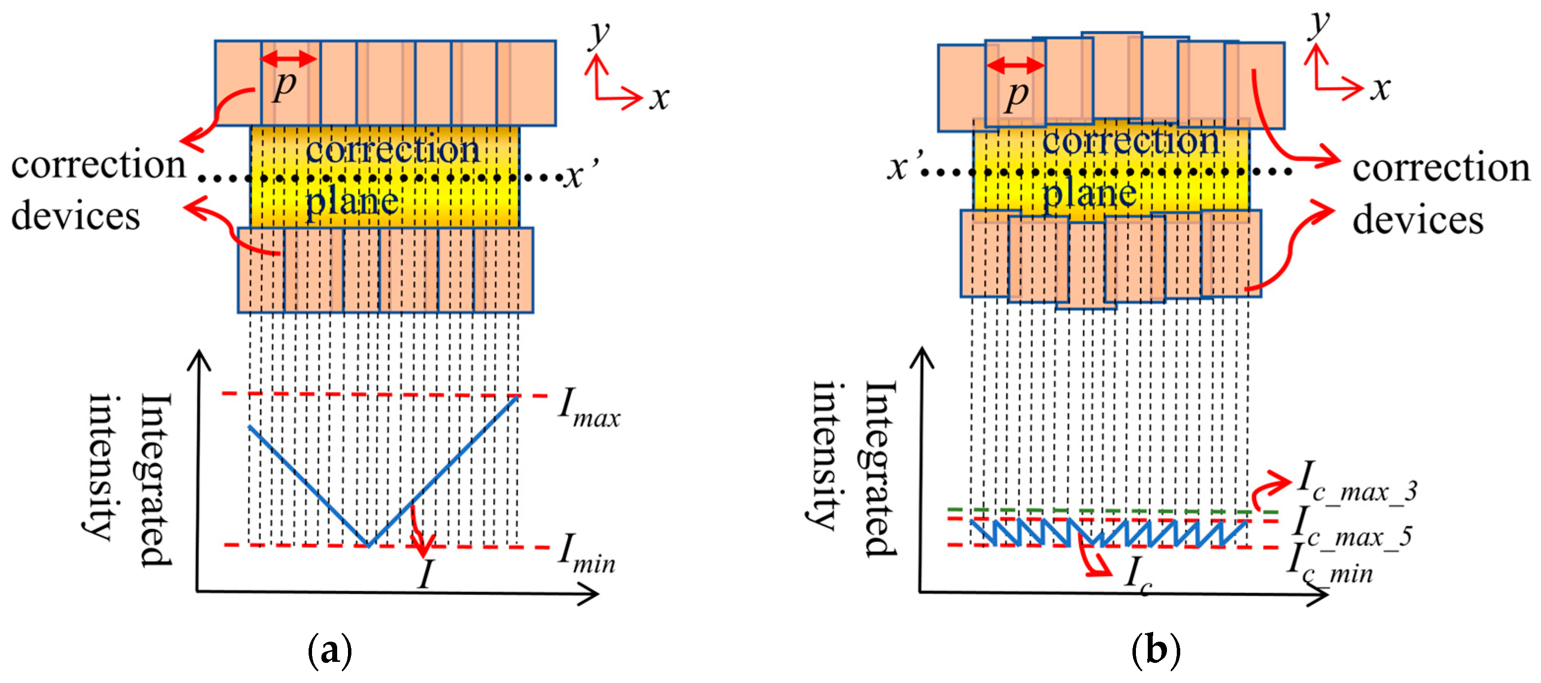
The structure of the two rows of units is changed from a symmetrical distribution along the x’-axis to an asymmetric distribution, as shown in Figure 6. In this case, the structure is staggered, so that the actual adjustable correction period of the units is reduced, which means the high-frequency integrated light intensity could be corrected to a lower position. This corresponds to Ic_max_3 in Figure 6b. Compared with the symmetrical arrangement, the staggered arrangement obviously improves the correction accuracy and has a more remarkable correction ability.
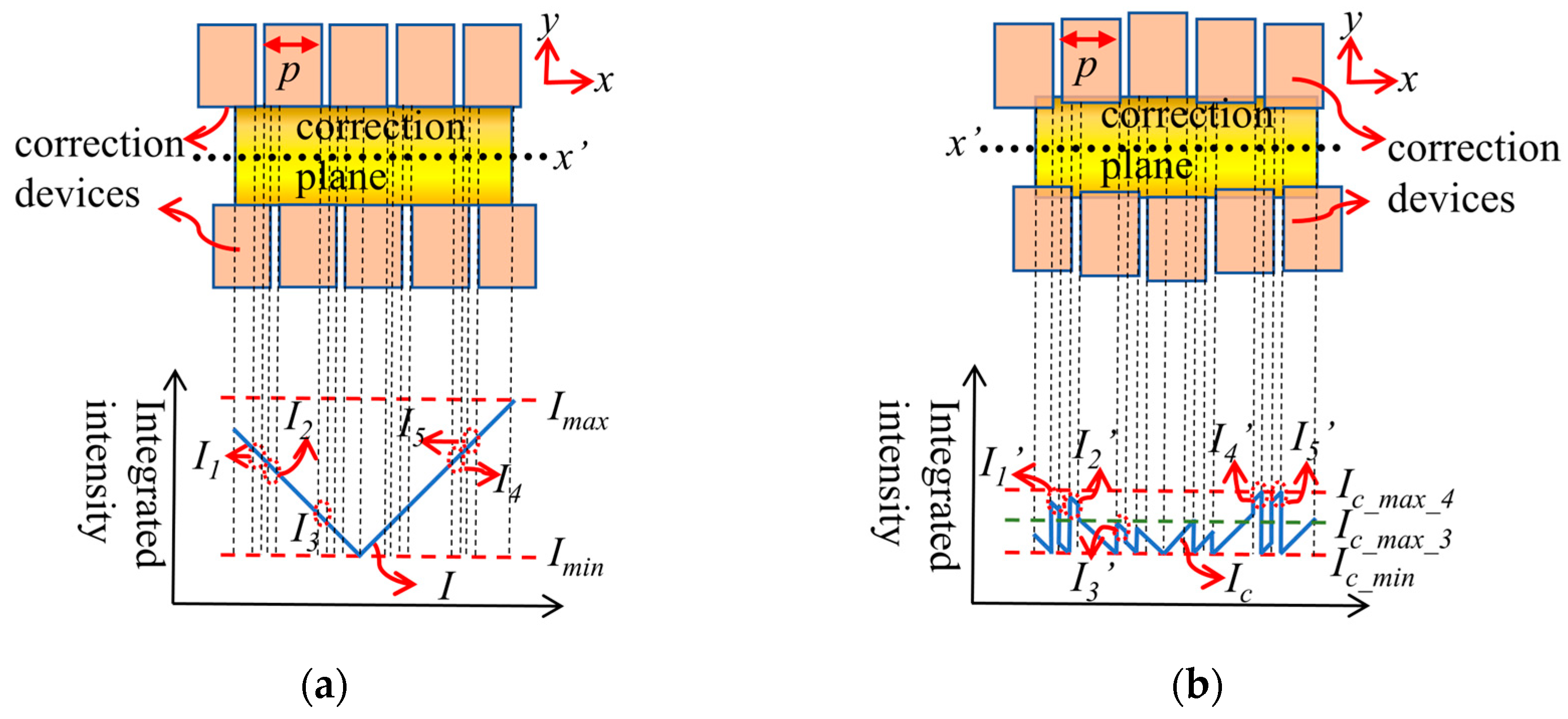
In the actual situation, the adjacent units need to move each other to leave a certain gap, as shown in Figure 7. The illumination field corresponding to the gap is not completely blocked by the finger unit, so the integrated light intensity curve will appear similar to the burr phenomenon, which means the integrated light intensity at the gap is not corrected to the ideal state. The integrated light intensity corresponding to the gap (I1, I2, I3, I4, I5) is corrected to the integrated light intensity corresponding to (I1, I2, I3, I4, I5). Since it is not corrected to the ideal value as expected, the maximum integrated light intensity Ic_max_4 after correction is higher than Ic_max_3. Due to the large high-frequency part of the integrated light intensity at the gap, the final corrected integrated uniformity effect is not ideal.

3. Design and Simulation Analysis

3.1. Design and Optimization Method of Uniformity Correction Device

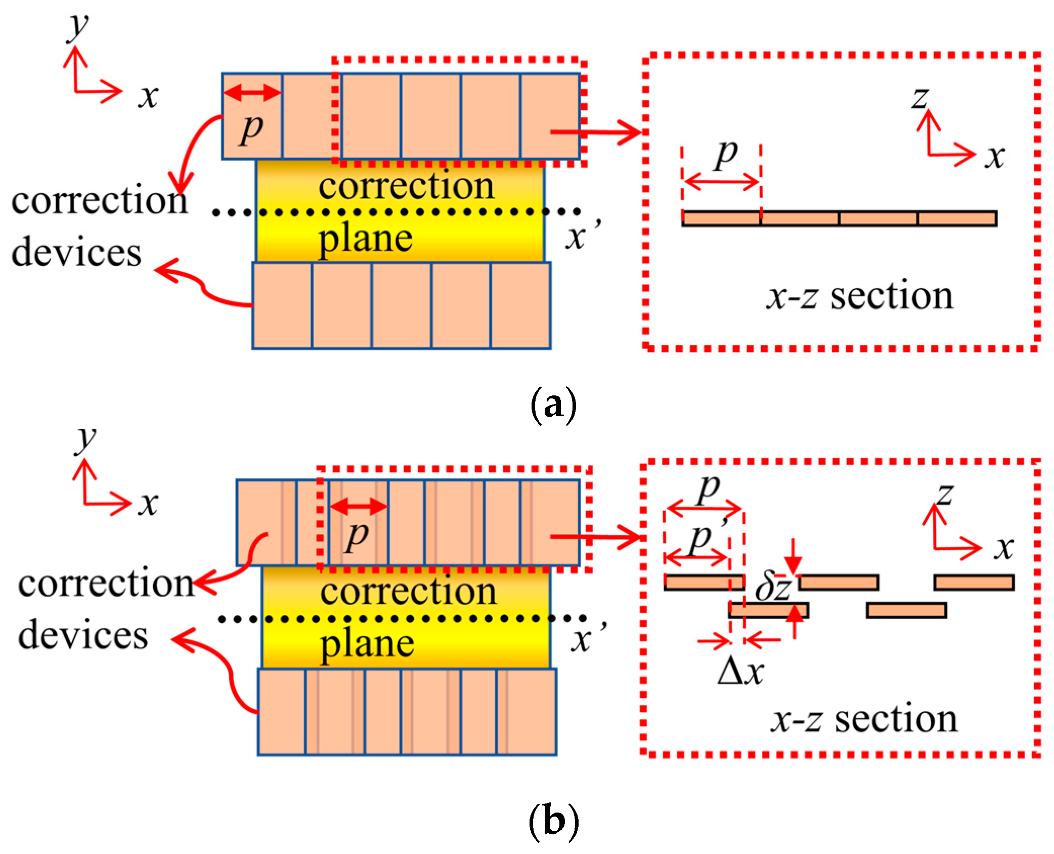
All finger units are arranged in the same plane, as shown in Figure 8a. Considering the existence of gaps, these gaps should be shielded in the design to avoid the adverse effects caused by gaps. Considering that each unit structure needs a separate control unit to control, if too many units are added to block the gap, it will greatly compress the operation space. This paper designs a structure that can avoid the negative impact of gaps and control the number of units. The units placed in a single row are placed in different planes in two layers, as shown in Figure 8b. The unit structure is placed in two layers, the interval between the two layers is δz, the size of the overlap of adjacent units is ∆x, and the width of the finger unit is p. The actual correction period width is p’. This arrangement can not only remove the gaps between adjacent units, but also cannot increase the number of units too much, which is also very beneficial to control the arrangement of the structure.
If the width of each unit is the same, but the layers overlap, the period width is reduced. According to the above analysis, the correction accuracy is higher when the period decreases. As shown in Figure 9, the planes of the two layers after stagging are different. In Figure 9, the interval between the planes of unit 1 and unit 2 is δz. For convenience of calculation, the pupil width blocked by the finger unit in the x’y’ plane corresponds to the pupil width in the x”y” plane, and the width of unit p2 in the plane of x”y”z projected to the width of the plane of x’y’z is p1, and the relationship between p1 and p2 is as below:
p 1 = p 2 Δ z / Δ z δ z
As long as it is satisfied that the value of p’ projected onto the x’y’ plane is smaller than the width p of the unit, a higher correction accuracy than that of the tiled structure can be achieved, and δz is satisfied.
δ z < Δ z p Δ z / p
Therefore, the unit structure placed in two layers has a higher correction accuracy than the unit structure tiled with the same width when δz satisfies Equation (9).
As shown in Figure 10, each row of units is divided into two overlapping layers, and the units on both sides of the x’-axis are asymmetrically arranged. Dividing each row into two layers can effectively eliminate the adverse effects caused by gaps, and under the same width of units, overlapping with each other can achieve a smaller period width. The finger units are divided into two layers with an asymmetric arrangement of two rows. It is able to further refine the actual period width of the unit, resulting in a higher correction accuracy. As shown in Figure 10b, a smaller correction period unit is able to correct the high-frequency integrated light intensity to a lower position (Ic_max_5), which means that this arrangement can achieve further improvement in the uniformity correction ability.
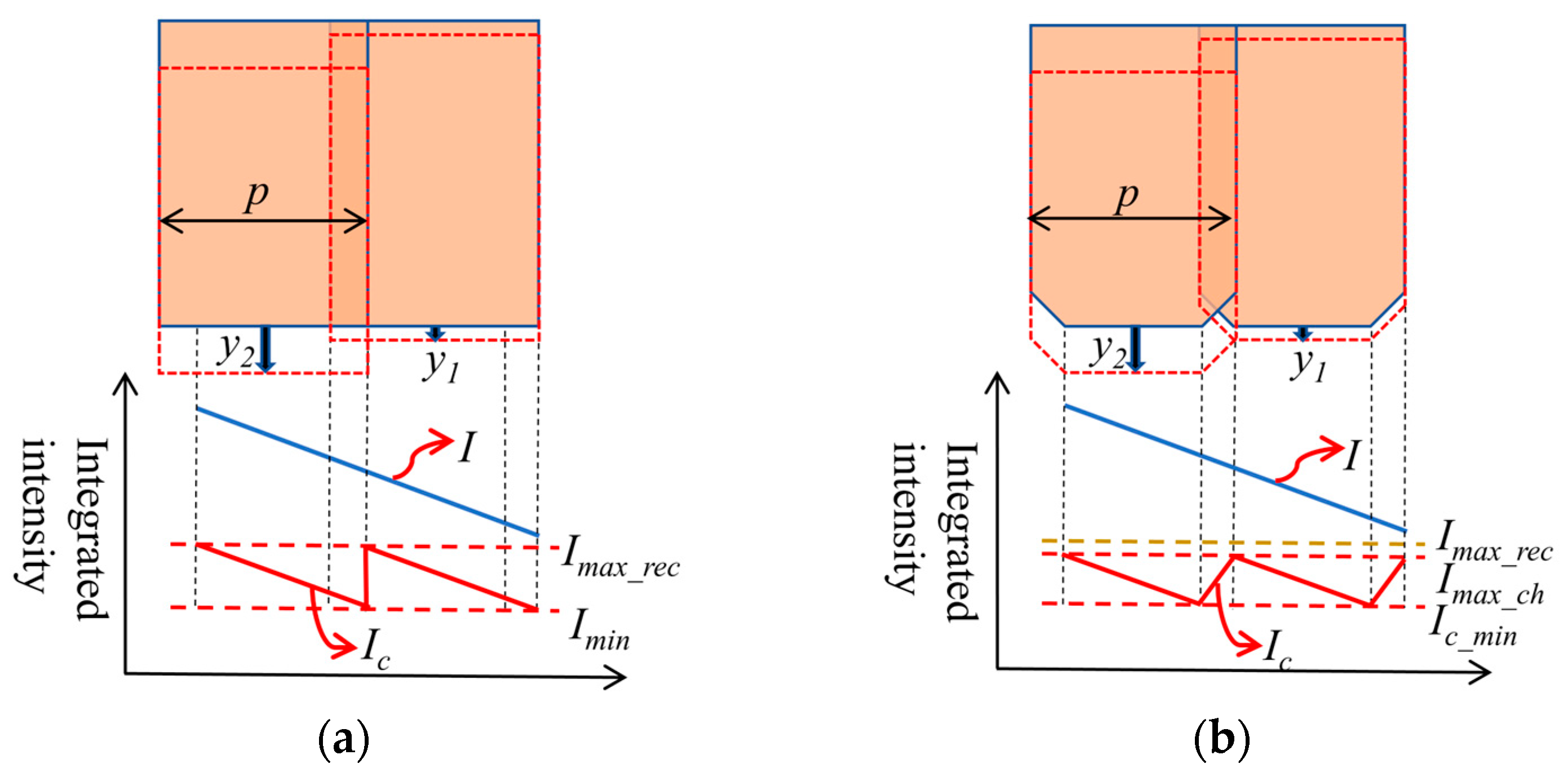
Considering the smaller width of the unit that corrects the finger array and the larger number of fingers, it becomes extremely difficult to control the arrangement of the driving units. In order to further improve the uniformity correction effect without increasing the number of units, both sides of the unit can be chamfered, as shown in Figure 11. After the chamfered unit is inserted into the illumination field, the area where the chamfered position is located can correct the larger integrated light intensity to a lower value, as shown in Figure 11b. This structure can have a better correction accuracy, and the addition of chamfering is equivalent to introducing a unit with a smaller period width, which can more accurately correct the size of the integrated light intensity, so as to further reduce the maximum integrated light intensity after correction. As shown in Figure 11b, the integrated light intensity curve is smoother, indicating that this structure has a better adjustment effect on the high-frequency part of the integrated light intensity. Therefore, compared with the unit without chamfering, the unit with chamfering has a certain degree of improvement in the correction ability.
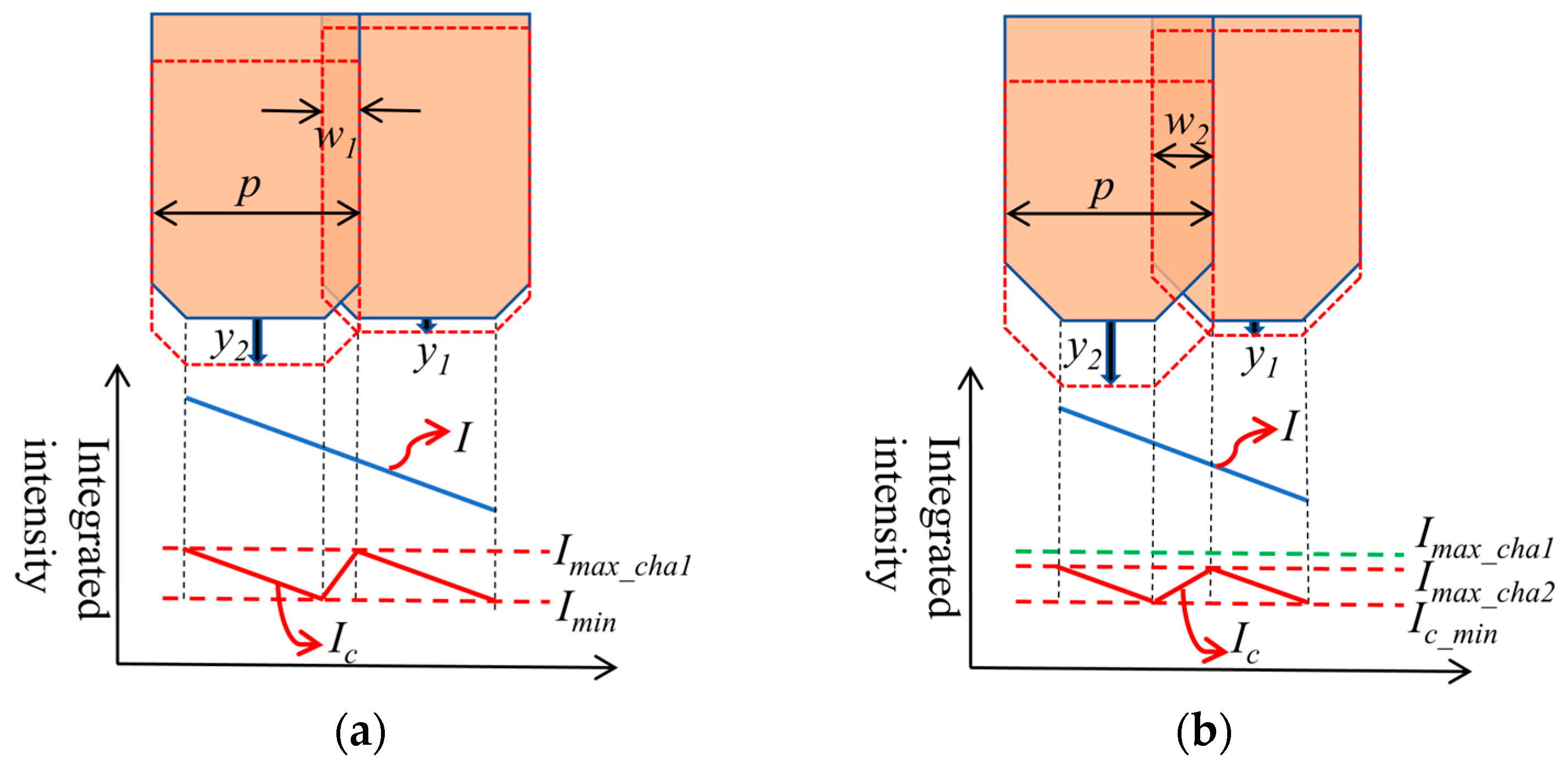
In order to determine the size of the chamfer, it is necessary to compare the correction effect of different chamfer sizes. When the width of the overlapping part of the two layers of the unit body is consistent with the chamfer size, the chamfer size of the front end of the unit body in Figure 12a is smaller than that of the front end of the unit body in Figure 12b. From the perspective of the correction effect, the correction accuracy of the larger chamfer size is higher. However, the chamfer size generally differs by more than half of the cell width, and because the size of the overlap of the two layers of units is the same as the chamfer size, as the chamfer size increases, the overlap will increase, which will lead to an increase in the number of cells.
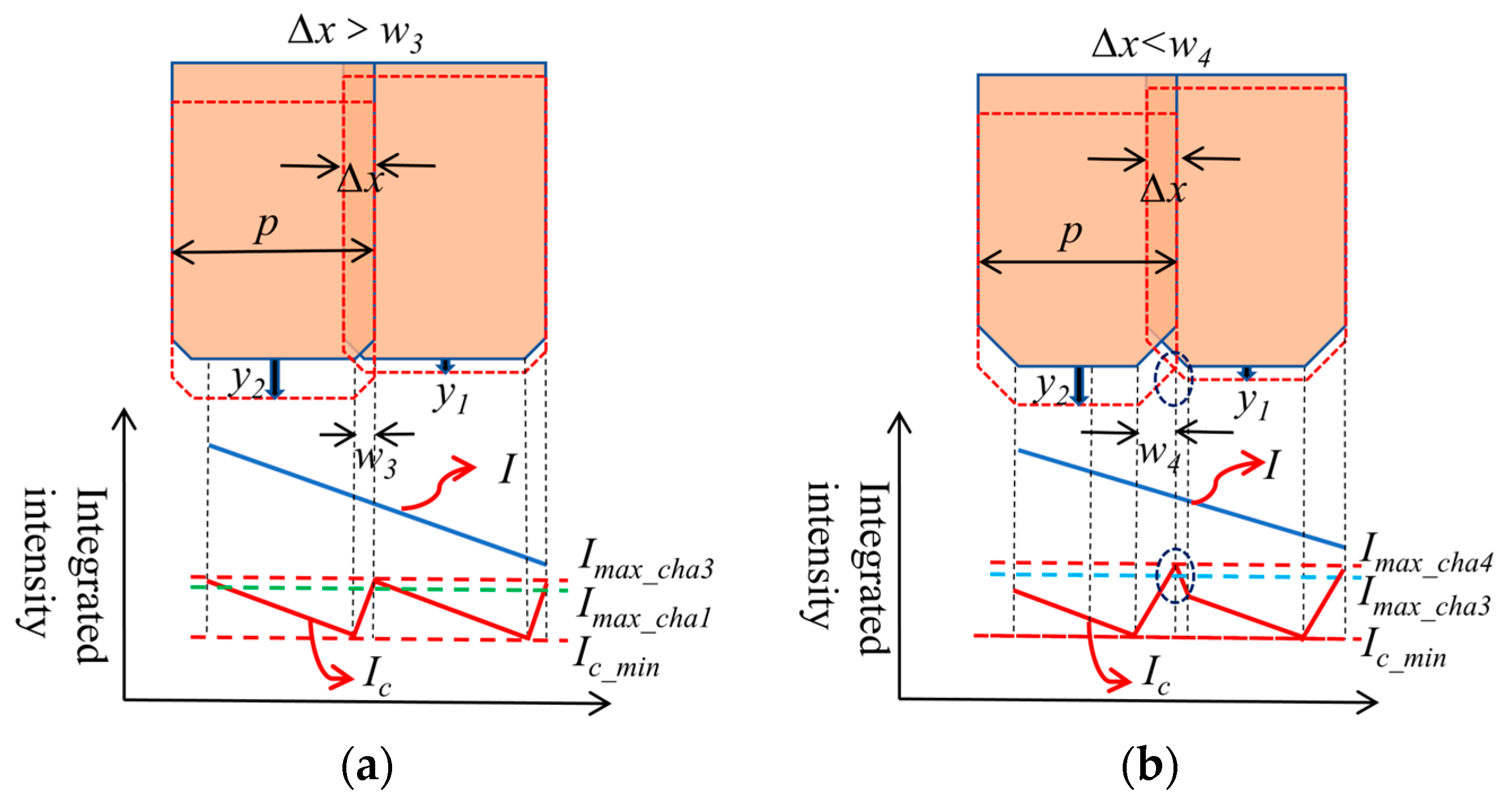
If the chamfer size is not consistent with the size of the overlapping part, the chamfer size w3 in Figure 13a is smaller than the unit overlap size ∆x (∆x = w1), and the chamfer size w4 in Figure 13b is larger than the unit overlap size ∆x. It can be seen that the correction accuracy when the chamfer size is not consistent with the size of the overlapping part is not as good as the correction accuracy when the width of the overlapping part of the two layers’ unit bodies is consistent with the chamfer size. For a smaller chamfer size than the unit overlap size, as in Figure 13a, Imax_cha3 is higher than Imax_cha1, for the width of the correction period is larger for real units. According to the previous analysis, the correction is better when the correction period width is smaller. For larger chamfer widths, as in Figure 13b, gaps may appear where the chamfers intersect, and a larger high-frequency part of integrated light intensity (Imax_cha4) may appear after correction. Therefore, the smoothness of the integrated light intensity curve corrected by a large chamfer size will be reduced, and the correction effect will become worse. Therefore, in order to ensure a consistent number of unit bodies, it is necessary to determine the size of the overlapping part first, and then set the chamfer to the same size as it.

3.2. Simulation Analysis

In order to verify the correction accuracy and correction ability of the uniformity correction device designed above, the designed device is simulated in the lithography illumination system. The partial structure model of the illumination system is shown in Figure 14 (It does not have to be this configuration). The illumination system uses an ArF excimer laser with a central wavelength of 193.37 nm as the light source, the numerical aperture of the image plane is 0.2325, and the size of the illumination field on the mask plane is 104 mm × 20 mm. The illumination modes include conventional illumination, annular illumination, and quadrupole illumination. The integrated nonuniformity of the illumination field at the mask plane is required to be below 0.3% for all illumination modes.
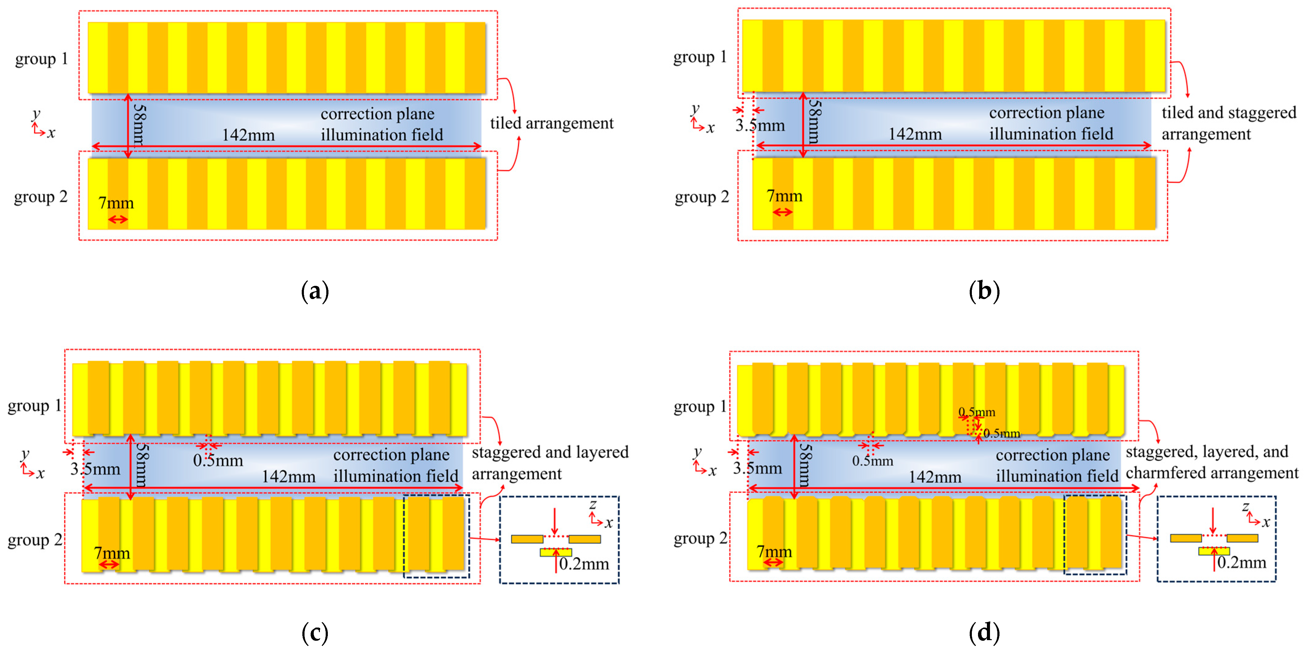
In the simulation, a distance of 90mm from the mask plane Δz is selected as the correction plane; the size of the illumination field in the correction plane is 142 mm × 58 mm. Considering the requirements of engineering practicability and uniformity correction, the width of the correction unit is set to 7 mm, which can meet the integrated nonuniformity requirement of being below 0.3%.
The units are divided into two rows on both sides of the scanning direction (y direction) and arranged symmetrically, with 20 in a single row and 40 in total, as shown in Figure 15a.
Figure 15b shows the tiled and staggered correction finger array structure. The width of each correction unit is 7 mm, the staggered distance between two rows of units is 3.5 mm, and the number of units in group 1 is 21 and in group 2 is 20, a total of 41 units.
Figure 15c shows the structure of units arranged in two layers along the z direction. The staggered distance between the two rows is 3.5 mm, and the interval between the two layers in each row is 0.2 mm, which is able to satisfy the requirements of Equation (9). The width of the overlap is 0.5 mm, the width of each unit is 7 mm, and the number of units in group 1 is 23 and in group 2 is 22, with a total of 45 units.
As shown in Figure 15d, both sides of each unit are chamfered, with a chamfer size of 0.5 mm × 45°, the same as the size of the overlap. The arrangement and number of units are consistent with those shown in Figure 15c.
Light tracing is performed on different illumination modes to the obtain illumination field of view and pupil data under different illumination modes. Figure 16 shows the visualization results. According to the illumination field data obtained by simulation, the optimal distance for each unit to move into the illumination field is calculated. The four finger array structures are, respectively, placed in the illumination system model of different modes, and then the ray tracing is carried out. The amount of light simulated by each uniformity correction device is consistent with that simulated without uniformity correction.
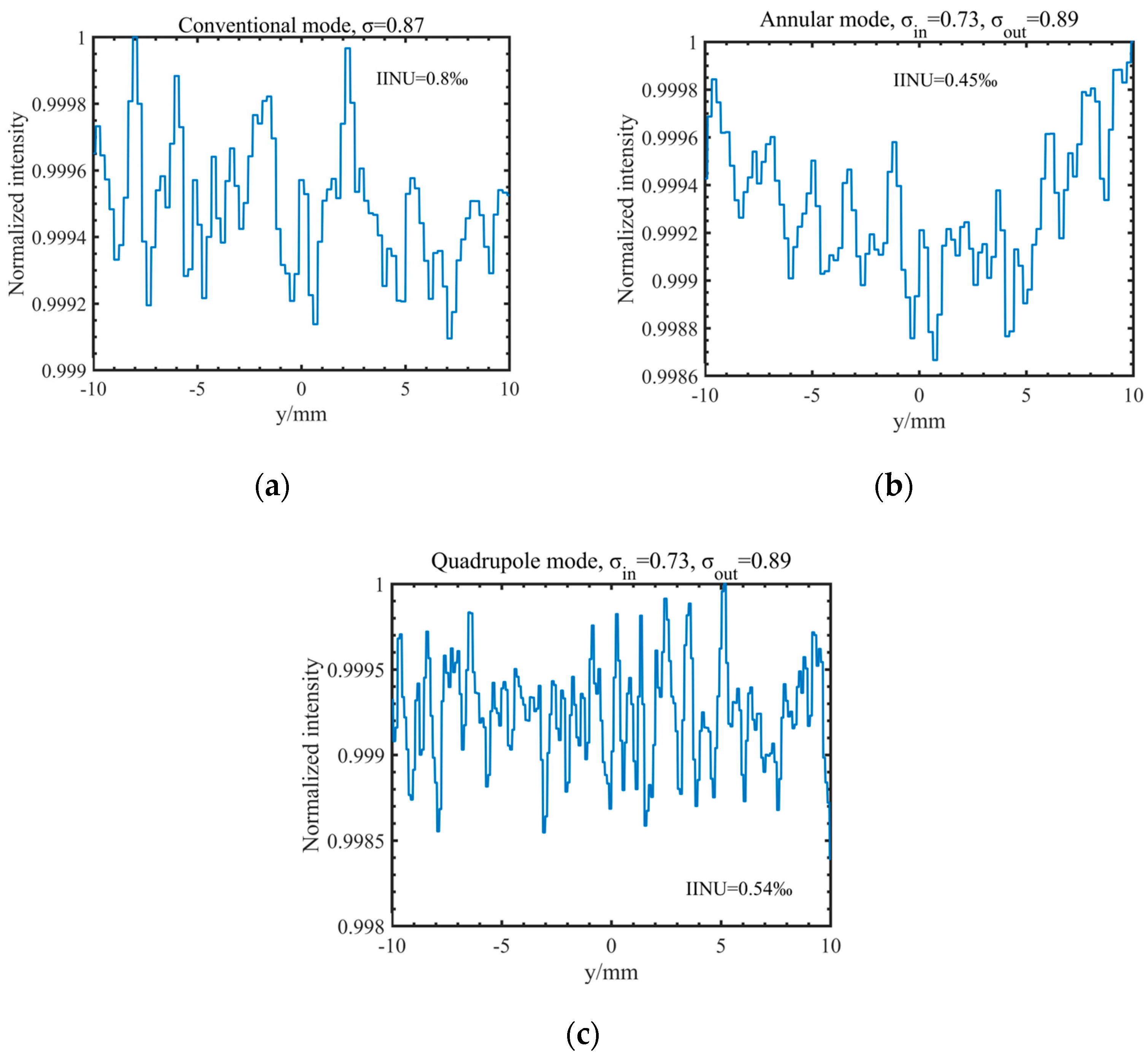
The scanning direction of the illumination field has a flat-top Gaussian distribution; therefore, the integrated light intensity in the x direction also has a flat-top Gaussian distribution. The integrated light intensity of the three illumination modes in the flat-top area in the x direction is shown in Figure 17; the integrated light intensity in this direction is evenly distributed, and the integrated nonuniformity is lower than 1‰. Therefore, the integrated light intensity in the x direction does not need to be corrected; only the integrated light intensity in the y direction needs to be corrected.
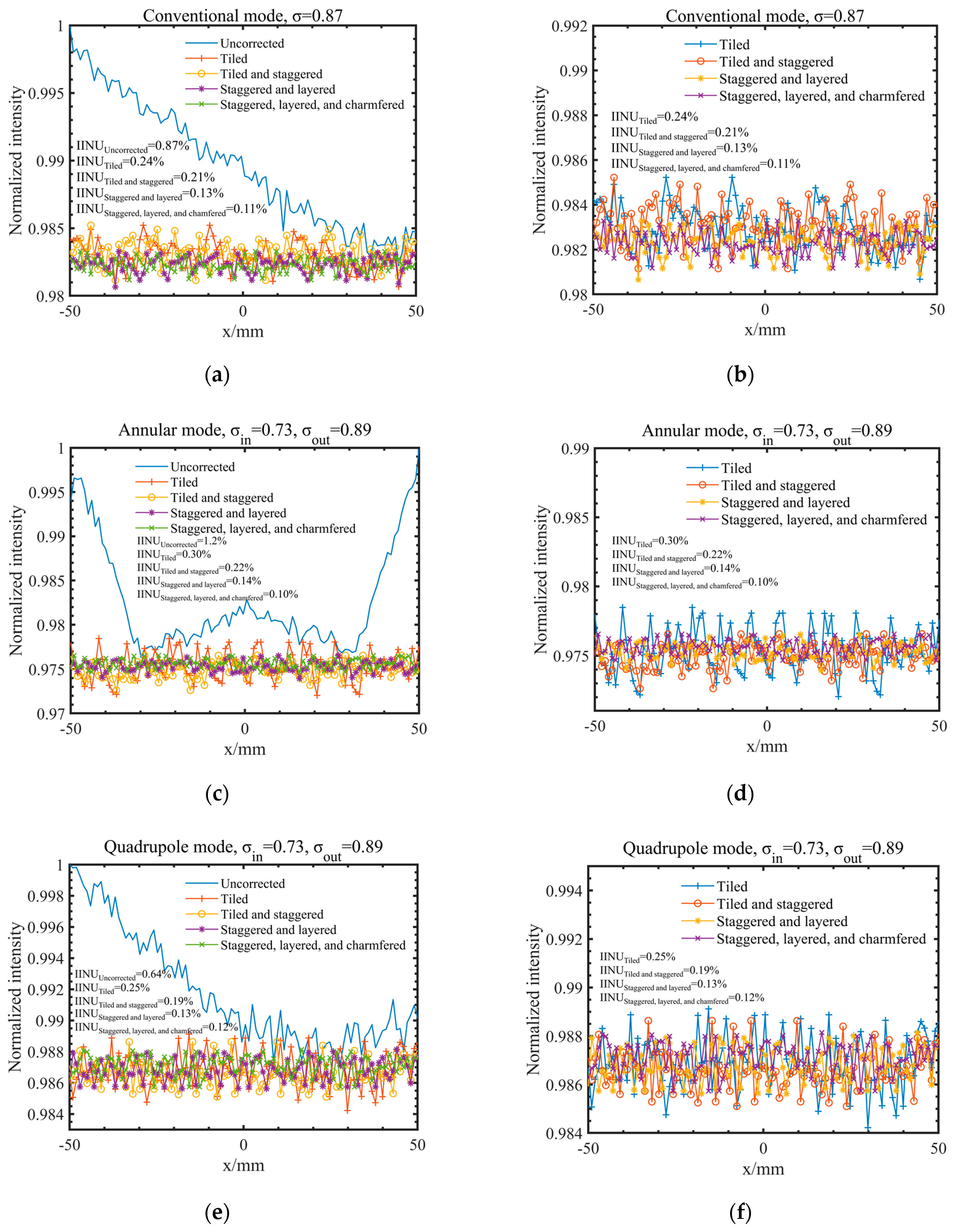
The simulation results are shown in Figure 18. In three different illumination modes, the four uniformity correctors have good correction effects on the integrated light intensity, and the integrated nonuniformity has reached the requirement of being 0.3% or below. From Figure 18b,d,f, comparing the tiled finger array, the tiled and staggered finger array corrected the high-frequency integrated light intensity better (corresponding to the red curve of Figure 18b,d,f) than the tiled non-staggered finger arrays (corresponding to the blue curve of Figure 18b,d,f). Compared with the previous two tiled finger arrays, the correction of the high-frequency part of the integrated light intensity arranged in interlacing layers (corresponding to the yellow and purple curves of Figure 18b,d,f) is more prominent, and the correction effect is significantly improved. Among them, the rectified integrated light intensity curve (corresponding to the purple curve of Figure 18b,d,f) of the finger array unit with chamfering is smoother than that of the rectangular unit. The simulation results show that a staggered arrangement can slightly improve the correction effect, a staggered and layered arrangement can greatly improve the correction effect, and after the finger unit is changed to have chamfering, that has a smooth effect for the integrated light intensity curve.
Table 1 summarizes the integrated nonuniformity data corresponding to the different rectified unit structures as well as the arrangement. It can be seen from Table 1 that the integrated nonuniformity of the tiled finger array after correction is better than 0.30%. The integrated nonuniformity of the tiled and staggered finger array after correction is better than 0.22%. The corrected integrated nonuniformity of the staggered and layered finger array is better than 0.14%. The corrected integrated nonuniformity of the staggered, layered, and chamfered layered finger array is better than 0.12%. In contrast, the layered finger array has a higher correction accuracy than the tiled finger array, and the integrated light intensity curve is smoother. The integrated nonuniformity of the finger array with the layered arrangement and chamfer is better than 0.12%.

4. Discussion

The uniformity correction device designed in this paper can be understood by the change in the periodic width of the unit in principle because of the layered arrangement. The period width of this layered arrangement is reduced compared to the arrangement within the same layer; according to the analysis, the smaller the period width, the higher the correction accuracy. In addition, if each unit is chamfered, the chamfer has a better control effect on the high-frequency part of the integrated light intensity, and the high-frequency component is further corrected, so the integrated light intensity curve is smoother. The above theoretical analysis is verified by simulation under different illumination modes.
In the original finger array structure, when ensuring a certain correction accuracy, it is necessary to closely arrange the two-layer unit, which also leads to the doubling of the number of units, which greatly increases the difficulty of the arrangement of the control units. In this paper, through appropriate arrangement and structural adjustment, the finger array has a higher correction accuracy for the illumination field, and the integral of the corrected light field is significantly reduced.
Since the finger array inserted into the illumination field is related to the calculation of the area, this in turn is related to the coherence factor of the illumination system. Compared with the conventional structure, as shown in Figure 15a, the number of finger arrays designed as shown in Figure 15c,d does not increase too much, so it will not increase the amount of calculation. The aforementioned advantages provide significant assistance in practical engineering applications. It is evident that the uniformity correction device provides substantial value for practical application.

5. Conclusions

In this study, the width, arrangement, and structure of the correction unit are analyzed. With the appropriate width of the correction unit, the arrangement of the correction unit and the shape of the unit are optimized, and a high-precision uniformity correction method suitable for the illumination field of the lithographic apparatus is proposed. In this paper, the principle of correcting the integrated uniformity of the illumination field of the lithographic apparatus with a different arrangement and structure for the same unit width is expounded. The feasibility of the method is verified by theoretical analysis and simulation. It can be seen from the simulation results that the staggered structure has a higher correction accuracy than the non-staggered structure for the same width of the unit, and the integrated nonuniformity is better than 0.22%. Compared with the same layered and staggered arrangement structure, the correction accuracy of the layered and staggered arrangement structure is improved to a certain extent, which is better than 0.14%. When chamfering is added to the front end of each unit, the integrated nonuniformity is better than 0.12%. Compared with the rectangular unit, the correction accuracy of the unit with chamfering is higher, and the corrected integrated light intensity curve is smoother.

Author Contributions

Conceptualization, S.L. and C.J.; methodology, J.L.; software, J.L.; validation, S.L. and C.J.; formal analysis, J.Z.; investigation, S.L.; resources, J.L.; data curation, J.Z.; writing—original draft preparation, S.L.; writing—review and editing, C.J.; visualization, S.L.; supervision, J.L.; project administration, J.L. All authors have read and agreed to the published version of the manuscript.

Funding

This research was funded by the Sichuan Science and Technology Program (2023JDRC0104). The work was supported by the National Key Research and Development Plan (2021YFB3200204), the National Natural Science Foundation of China (NSFC) under grant nos. 61604154, 61775201, 61975211, and 62005287, the Youth Innovation Promotion Association of the Chinese Academy of Sciences (2021380), the project of the Western Light of Chinese Academy of Science (YA23K056), and the Sichuan Science and Technology Program (2023JDRC0104), the Sichuan Provincial Regional Innovation Cooperation Project (2024YFHZ0189), the Sichuan Provincial Science Fund for Distinguished Young Scholars (2024NSFJQ0027).

Institutional Review Board Statement

This study excludes this statement.

Informed Consent Statement

Not applicable.

Data Availability Statement

The data of this project are temporarily withheld for special reasons.

Conflicts of Interest

The authors declare no conflicts of interest.

References

  1. Thompson, L.F. An Introduction to Lithography; ACS Publications: Washington, DC, USA, 1983. [Google Scholar]
  2. Liu, J.; Zhang, F.; Huang, H. Research Progress on Illumination System Technology of Step-and-Scan Projection Lithography Tools. Laser Optoelectron. Prog. 2022, 59, 09220111. [Google Scholar] [CrossRef]
  3. Stagaman, G.J.; Eakin, R.J.; Sardella, J.C.; Johnson, J.R.; Spinner III, C.R. Effects of complex illumination on lithography performance. In Proceedings of the Optical Microlithography IX, Santa Clara, CA, USA, 13–15 March 1996; pp. 146–157. [Google Scholar]
  4. Antoni, M.; Singer, W.; Schultz, J.; Wangler, J.; Escudero-Sanz, I.; Kruizinga, B. Illumination optics design for EUV lithography. In Proceedings of the Soft X-ray and EUV Imaging Systems, San Diego, CA, USA, 3–4 August 2000; pp. 25–34. [Google Scholar]
  5. van Schoot, J.; Noordman, O.; Vanoppen, P.; Blok, F.; Yim, D.; Park, C.H.; Cho, B.H.; Theeuwes, T.; Min, Y.H. CD uniformity improvement by active scanner corrections. In Proceedings of the Optical Microlithography XV Conference, Santa Clara, CA, USA, 5–8 March 2002; pp. 304–314. [Google Scholar]
  6. Chua, G.S.; Eran, C.; Tan, S.K.; Choi, B.I.; Ng, T.H.; Lua, P.L.; Sharoni, O.; Ben-Zvi, G. Intra Field CD Uniformity Correction by Scanner Dose Mapper™ using Galileo® Mask Transmission Mapping as the CDU Data Source. In Proceedings of the Conference on Optical Microlithography XXIII, San Jose, CA, USA, 23–25 February 2010. [Google Scholar]
  7. Dusa, M.; Moerman, R.; Singh, B.; Friedberg, P.; Hoobler, R.; Zavecs, T. Intra-wafer CDU characterization to determine process and focus contributions based on Scatterometry Metrology. In Proceedings of the Data Analysis and Modeling for Process Control, Santa Clara, CA, USA, 26–27 February 2004; pp. 93–104. [Google Scholar]
  8. van der Laan, H.; Carpaij, R.; Krist, J.; Noordman, O.; van Dommelen, Y.; van Schoot, J.; Blok, F.; van Os, C.; Stegeman, S.; Hoogenboom, T. Etch, reticle, and track CD fingerprint corrections with local dose compensation. In Proceedings of the Data Analysis and Modeling for Process Control II, San Jose, CA, USA, 3–4 March 2005; pp. 107–118. [Google Scholar]
  9. Buttgereit, U.; Birkner, R.; Joyner, M.; Graitzer, E.; Cohen, A.; Miyashita, H.; Triulzi, B.; Zeballos, A.F.; Romeo, C. CD uniformity correction on 45-nm technology non-volatile memory. In Proceedings of the Metrology, Inspection, and Process Control for Microlithography XXIV, San Jose, CA, USA, 22–25 February 2010; pp. 1121–1129. [Google Scholar]
  10. Chen, M.; Chen, L.Q.; Zeng, A.J.; Zhu, J.; Yang, B.X.; Huang, H.J. Generation of trapezoidal illumination for the step-and-scan lithographic system. Appl. Opt. 2015, 54, 6820–6826. [Google Scholar] [CrossRef] [PubMed]
  11. Chen, M.; Wang, Y.; Zeng, A.; Zhu, J.; Yang, B.; Huang, H. Flat Gauss illumination for the step-and-scan lithographic system. Opt. Commun. 2016, 372, 201–209. [Google Scholar] [CrossRef]
  12. Guo, L.; Huang, H.; Wang, X. Study of Integrator Rod in Step-and-scan Lithography. Acta Photonica Sin. 2006, 35, 981–985. [Google Scholar]
  13. Voelkel, R.; Vogler, U.; Bich, A.; Pernet, P.; Weible, K.J.; Hornung, M.; Zoberbier, R.; Cullmann, E.; Stuerzebecher, L.; Harzendorf, T.; et al. Advanced mask aligner lithography: New illumination system. Opt. Express 2010, 18, 20968–20978. [Google Scholar] [CrossRef] [PubMed]
  14. Xiao, L.; Li, Y.; Wei, L. Design of chirped fly’s eye uniformizer for ArF lithography illumination system. In Proceedings of the International Symposium on Optoelectronic Technology and Application 2014: Advanced Display Technology; Nonimaging Optics: Efficient Design for Illumination and Solar Concentration, Beijing, China, 13–15 May 2014; pp. 152–158. [Google Scholar]
  15. Ma, X.; Zhang, F.; Niu, Z.; Huang, H. Design and optimization of top-Gaussian illumination field in photolithography. Opt. Eng. 2021, 60, 025106. [Google Scholar] [CrossRef]
  16. Brandt, R.J. Uniform Light Intensity Providing Apparatus for Use during Solar Panel Testing, Has Uniformity Filter in One of Light Baffles in Which Lot of Wires Are Diagonally Disposed in Each Zone. U.S. Patent No. 6,076,942, 20 June 2000. [Google Scholar]
  17. Gong, S.; Yang, B.; Huang, H. Illumination uniformity correction by using dynamic gray filters in a lithography system. Appl. Opt. 2022, 61, 2706–2714. [Google Scholar] [CrossRef]
  18. Zimmerman, R.C.; Van Greevenbroek, H.R.M.; Kochersperger, P.C.; Downey, T.R.; Stone, E.; Csiszar, S.I.; Kubick, F.; Vladimirsky, O. Lithographic Apparatus and Method for Illumination Uniformity Correction and Uniformity Drift Compensation. U.S. Patent No. 8,629,973, 14 January 2014. [Google Scholar]
  19. Zimmerman, R.C. Double EUV Illumination Uniformity Correction System and Method. U.S. Patent No. 9,134,620, 15 September 2015. [Google Scholar]
  20. Cheng, W.; Zhang, F.; Lin, D.; Zeng, A.; Yang, B.; Huang, H. High Precision Correction Method of Illumination Field Uniformity for PhotolithographyIllumination System. Acta Opt. Sin. 2018, 38, 0722001. [Google Scholar] [CrossRef]
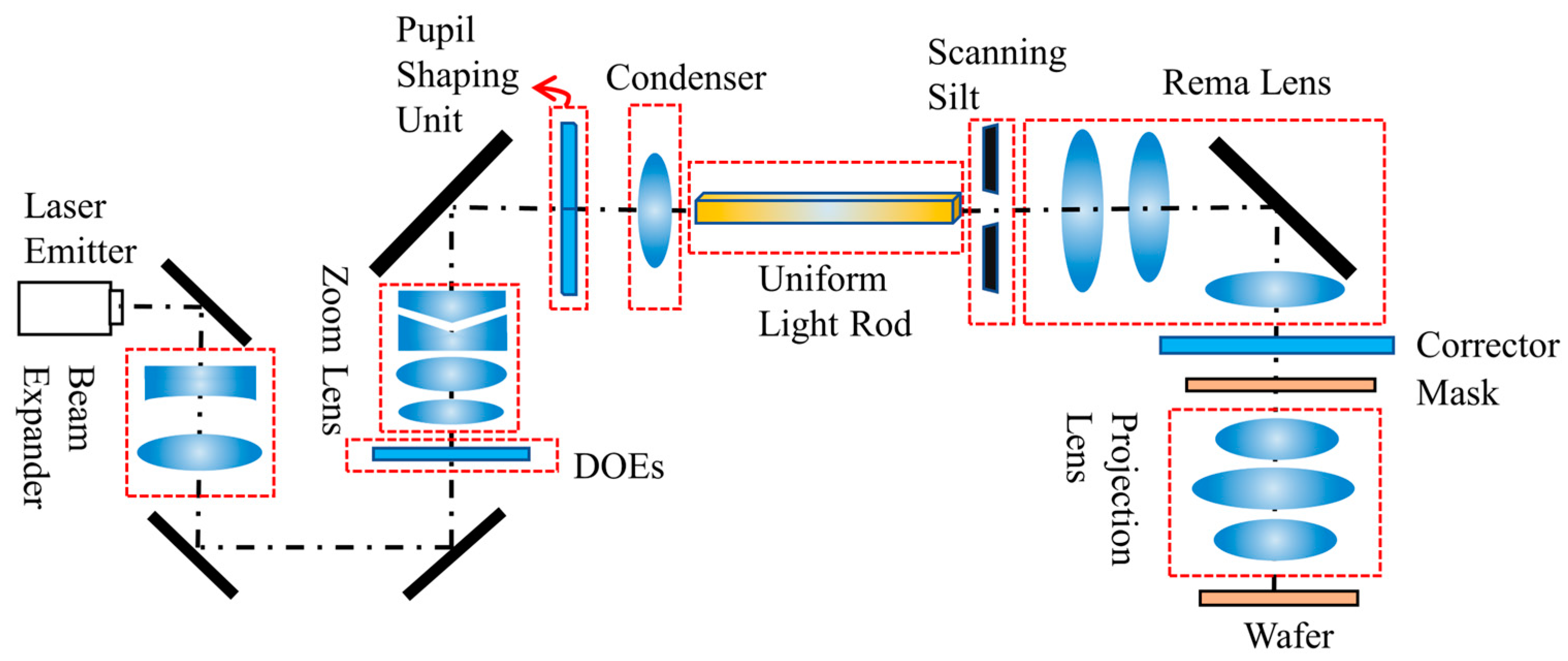
Figure 1. Schematic diagram of step-scanning lithography illumination system.
Photonics 11 00661 g001
Figure 2. Flat-top Gaussian illumination field.
Photonics 11 00661 g002
Figure 3. Illumination pupil. (a) Conventional; (b) annular; (c) quadrupole.
Photonics 11 00661 g003
Figure 4. Schematic diagram of finger array.
Photonics 11 00661 g004
Figure 5. Diagram of integrated uniformity of corrected illumination field of different unit width. (a) Integrated intensity contrast before and after correction for unit width p; (b) integrated intensity contrast before and after correction for smaller unit width p’.
Photonics 11 00661 g005
Figure 6. Diagram of correcting integrated uniformity of staggered distributed finger array. (a) Uncorrected; (b) corrected.
Photonics 11 00661 g006
Figure 7. Schematic diagram of the uniformity correction result for the gaps between finger arrays. (a) Uncorrected; (b) corrected.
Photonics 11 00661 g007
Figure 8. Schematic diagram of finger array with two arrangement modes. (a) Tiled and staggered; (b) staggered and layered.
Photonics 11 00661 g008
Figure 9. Schematic diagram of the uniformity principle of layered structure correction. (a) Comparison of the area of the same pupil blocked by the same finger unit in different planes; (b) the relationship between p1 and p2.
Photonics 11 00661 g009
Figure 10. Diagram of uniformity correction results for staggered and layered finger arrays. (a) Uncorrected; (b) corrected.
Photonics 11 00661 g010
Figure 11. Correction effect of different front-end structures of finger array units. (a) Rectangle; (b) chamfered.
Photonics 11 00661 g011
Figure 12. Correction effect of different chamfer sizes at the unit’s front end when the chamfer size is consistent with the overlap size. (a) Smaller chamfer size w1; (b) larger chamfer size w2.
Photonics 11 00661 g012
Figure 13. Correction effect of different chamfer sizes at the unit’s front end when the chamfer and overlap sizes are not consistent. (a) Chamfer size w3 is smaller than overlap width ∆x (∆x = w1); (b) chamfer size w4 is larger than overlap width ∆x.
Photonics 11 00661 g013
Figure 14. Part-structure simulation model of lithography illumination system.
Photonics 11 00661 g014
Figure 15. The structure diagram of finger arrays with four different structures and arrangements. (a) Tiled; (b) tiled and staggered; (c) staggered and layered; (d) staggered, layered, and chamfered.
Photonics 11 00661 g015
Figure 16. The illumination field image and pupil image obtained by simulation. (a) Conventional, σ = 0.87; (b) annular, σin = 0.73, σout = 0.89; (c) quadrupole, σin = 0.73, σout = 0.89.
Photonics 11 00661 g016
Figure 17. Integrated light intensity of x direction for three illumination modes. (a) Conventional mode, σ = 0.87; (b) annular mode, σin = 0.73, σout = 0.89; (c) quadrupole mode, σin = 0.73, σout = 0.89.
Photonics 11 00661 g017
Figure 18. Uncorrected and corrected integrated light intensity of y direction for three illumination modes. (a,b) Conventional mode, σ = 0.87; (c,d) annular mode, σin = 0.73, σout = 0.89; (e,f) quadrupole mode, σin = 0.73, σout = 0.89.
Photonics 11 00661 g018
Table 1. Summary of integrated uniformity uncorrected and corrected for three illumination modes.
Illumination ModeUncorrected Integrated NonuniformityCorrected Integrated Nonuniformity
TiledTiled and StaggeredStaggered and LayeredStaggered, Layered, and Chamfered
Conventionalσ = 0.870.87%0.24%0.21%0.13%0.11%
Annularσin = 0.73, σout = 0.891.20%0.30%0.22%0.14%0.10%
Quadrupoleσin = 0.73, σout = 0.890.64%0.25%0.19%0.13%0.12%
Disclaimer/Publisher’s Note: The statements, opinions and data contained in all publications are solely those of the individual author(s) and contributor(s) and not of MDPI and/or the editor(s). MDPI and/or the editor(s) disclaim responsibility for any injury to people or property resulting from any ideas, methods, instructions or products referred to in the content.